


6276
16-BIT SERIAL-INPUT, CONSTANTCURRENT LATCHED LED DRIV ER
26185.201E
Data Sheet
A6276ELW
GROUND
SERIAL
DATA IN
ENABLE
1
2
CLOCK CK
3
LATCH
4
OUT
5
0
OUT
6
1
OUT
7
2
8 17
OUT
3
9
OUT
4
OUT
10
5
OUT
11
6
12
OUT
7
REGULATOR
L
REGISTER
LATCHE S
V
I
O
Note that three packages offered are electrically
identical and share a common terminal number assignment.
LOGIC
24
DD
SUPPLY
R
23
EXT
SERIAL
22
DATA OUT
OUTPUT
21
OE
ENABLE
20
OUT
15
OUT
19
14
18
OUT
13
OUT
12
OUT
16
11
OUT
15
10
OUT
14
9
13
OUT
8
Dwg. PP-029-1 1
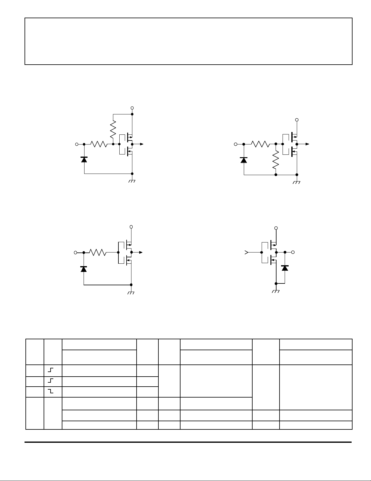
ABSOLUTE MAXI MUM RATINGS
Supply Voltage, VDD ....................... 7.0 V
Output Voltage Range,
............................. -0.5 V to +17 V
V
O
Output Current, I
Ground Current, I
Input Voltage Range,
.................... -0.4 V to VDD + 0.4 V
V
I
Package Power Dissipation,
..................................... See Graph
P
D
Operating T emperature Range,
............................. -40°C to +85°C
T
A
Storage T emperature Range,
........................... -55°C to +150°C
T
S
Caution: These CMOS devices have input static
protection (Class 2) but are still sus cep ti ble
to damage if exposed to extremely high static
electrical charges.
........................ 90 mA
O
.............. 1475 mA
GND
The A6276 is specifically designed for LED-display applications.
Each BiCMOS device includes a 16-bit CMOS shift register, accompanying data latches, and 16 npn constant-current sink drivers. Except
for package style and allowable package power dissipation, the device
options are identical.
The CMOS shift register and latches allow direct interfacing with
microprocessor-based systems. With a 5 V logic supply, typical serial
data-input rates are up to 20 MHz. The LED drive current is de ter mined by the user’s selection of a single resistor. A CMOS serial data
output permits cascade connections in applications requiring additional
drive lines. For inter-digit blanking, all output drivers can be disabled
with an ENABLE input high. Similar 8-bit devices are available as the
A6275EA and A6275ELW.
Three package styles are provided: through-hole DIP (suffix A),
surface-mount SOIC (suffix LW) and TSSOP with exposed thermal pad
(suffix LP). Under normal applications, a copper lead frame and low
logic-power dissipation allow the dual in-line package to sink maximum rated current through all outputs con tin u ous ly over the operating
temperature range (90 mA, 0.75 V drop, +85°C).
FEATURES
■ To 90 mA Constant-Current Outputs
■ Under-Voltage Lockout
■ Low-Power CMOS Logic and Latches
■ High Data Input Rate
■ Functional Replacement for TB62706BN/BF
Selection Guide
Part Number Pb-free* Package Packing
A6276EA-T Yes 24-pin DIP 15 per tube –40 to 85
A6276ELP-T Yes 24-pin TSSOP 62 per tube –40 to 85
A6276ELPTR-T Yes 24-pin TSSOP 4000 per reel –40 to 85
A6276ELW-T Yes 24-pin SOICW 31 per tube –40 to 85
A6276ELWTR-T Yes 24-pin SOICW 1000 per reel –40 to 85
A6276SLW-T Yes 24-pin SOICW 31 per tube –20 to 85
A6276SLWTR-T Yes 24-pin SOICW 1000 per reel –20 to 85
*Pb-based variants are being phased out of the product line. The variants cited in this
footnote are in production but have been determined to be NOT FOR NEW DESIGN.
This classification indicates that sale of this device is currently restricted to existing
customer applications. The variants should not be purchased for new design applications because obsolescence in the near future is probable. Samples are no longer
available. Status change: May 1, 2006. These variants include:A6276EA, A6276ELW,
A6276ELWTR, A6276SA, A6276SLW, and A6276SLWTR.
Ambient
Temperature (°C)
6276
16-BIT SERIAL-INPUT,
CONSTANT-CURRENT
LATCHED LED DRIV ER
4.0
3.5
3.0
2.5
2.0
1.5
1.0
0.5
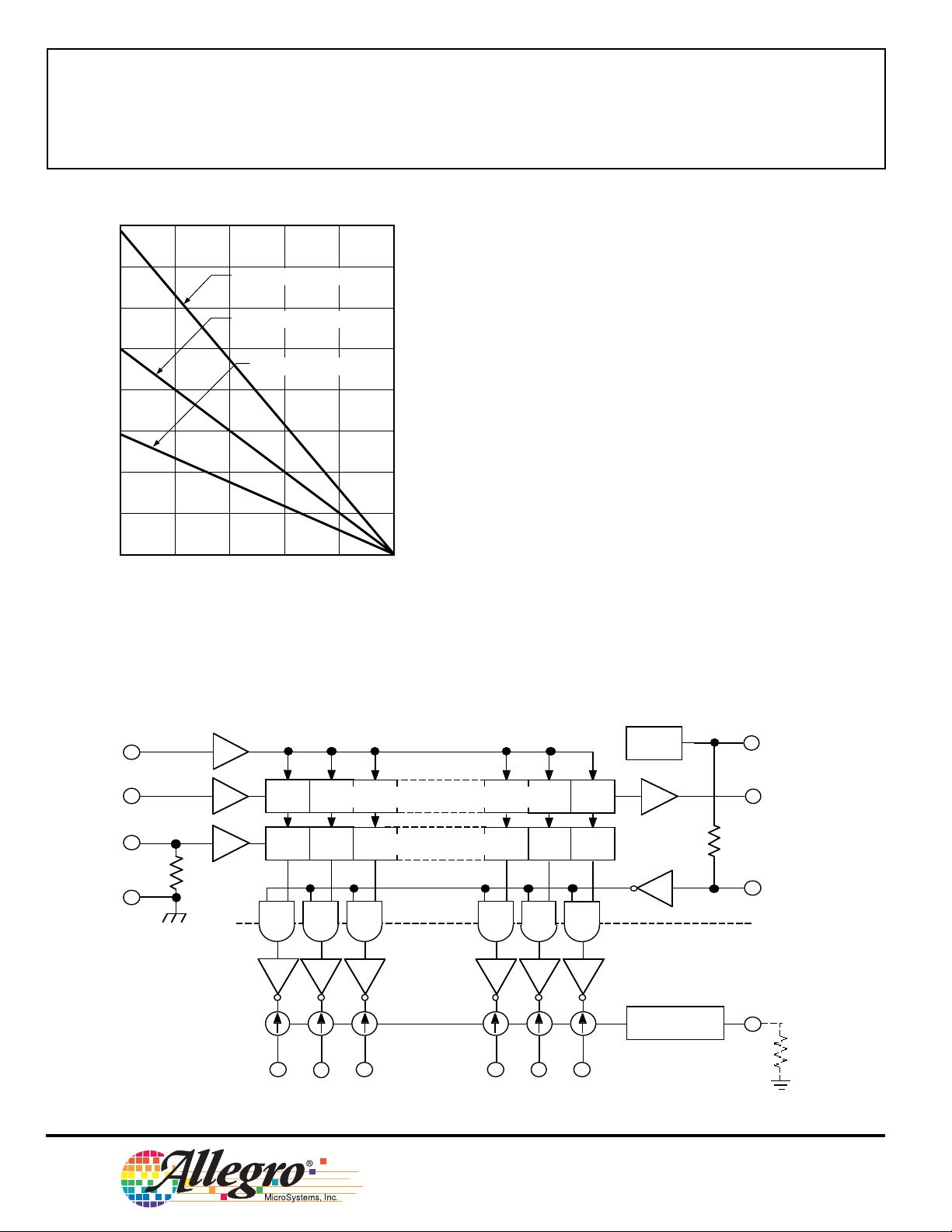
ALLOWABLE PACKAGE POWER DISSIPATION IN WATTS
0
25
*Mounted on single-layer, two-sided PCB, with 3.8 in2copper each side;
additional information on Allegro Web site
50 75 100 125 150
AMBIENT TEMPERATURE IN °°°°C
24-PIN TSSOP*, R
24-PIN DIP, R
θJA
24-LEAD SOIC, R
θJA
=32°C/W
=50°C/W
θJA
= 85°C/W
FUNCTIONAL BLOCK DI A GRAM
CLOCK
SERIAL
DATA IN
LATCH
ENABLE
GROUND
2
OUT0OUT
SERIAL-PARALLEL SHIFT REGISTER
LATCHES
OUT
1
2
115 Northeast Cutoff, Box 15036
Worcester, Massachusetts 01615-0036 (508) 853-5000
Copyright © 2000, 2003 Allegro MicroSystems, Inc.
OUT
N
UVLO
BIPOLAR
I
O
REGULATOR
V
DD
MOS
LOGIC
SUPPLY
SERIAL
DATA OUT
OUTPUT ENABLE
(ACTIVE LOW)
R
EXT
Dwg. FP-013-3
6276
DD
16-BIT SERIAL-INPUT,
CONSTANT-CURRENT
LATCHED LED DRIVER
V
DD
V
DD
IN
Dwg. EP-010-11
IN
Dwg. EP-010-12
LATCH ENABLEOUTPUT ENABLE (active low)
V
DD
IN
Dwg. EP-063-6
Dwg. EP-010-13
V
OUT
CLOCK and SERIAL DATA IN SERIAL DATA OUT
TRUTH TABLE
Serial Shift Register Contents Serial Latch Latch Contents Output Output Contents
Data Clock Data Enable Enable
Input Input I
1I2I3
HHR
LLR
XR
1R2R3
XXX...X X X L R1R2R3... R
P1P2P3... P
L = Low Logic (Voltage) Level H = High Logic (Voltage) Level X = Irrelevant P = Present State R = Previous State
www.allegromicro.com
1R2
1R2
... I
... R
... R
... R
N-1IN
N-2RN-1
N-2RN-1
N-1RN
N-1PN
Output Input I1I2I3... I
R
N-1
R
N-1
R
N
P
N
HP1P2P3... P
XXX...X X H H H H ... H H
N-1IN
N-1 RN
N-1 PN
Input I1I2I3... I
LP1P2P3... P
I
N-1
N-1 PN
N
3
6276
16-BIT SERIAL-INPUT,
CONSTANT-CURRENT
LATCHED LED DRIVER
ELECTRICAL CHARACTERISTICS at T
= +25°C, V
A
= 5 V (unless otherwise noted).
DD
Limits
Characteristic Symbol Test Conditions Min. Typ. Max. Unit
Supply Voltage Range V
Under-Voltage Lockout V
Output Current I
DD
DD(UV)
O
(any single output)
Output Current Matching ∆I
O
(difference between any R
two outputs at same VCE)
Output Leakage Current I
Logic Input Voltage V
SERIAL DATA OUT V
Voltage
CEX
V
V
IH
IL
OL
OH
Operating 4.5 5.0 5.5 V
V
= 0 → 5 V 3.4 – 4.0 V
DD
VCE = 0.7 V, R
VCE = 0.7 V, R
0.4 V ≤ V
V
OH
I
OL
I
OH
CE(A)
EXT
R
EXT
= 15 V – 1.0 5.0 µA
= 500 µA – – 0.4 V
= -500 µA 4.6 – – V
= 250 Ω 64.2 75.5 86.8 mA
EXT
= 470 Ω 34.1 40.0 45.9 mA
EXT
= V
CE(B)
≤ 0.7 V:
= 250 Ω – ±1.5 ±6.0 %
= 470 Ω – ±1.5 ±6.0 %
0.7V
GND – 0.3V
–VDDV
DD
DD
V
Input Resistance R
I
ENABLE Input, Pull Up 150 300 600 kΩ
LATCH Input, Pull Down 100 200 400 kΩ
Supply Current I
DD(OFF)
I
DD(ON)
R
= open, VOE = 5 V – 0.8 1.4 mA
EXT
R
= 470 Ω, V
EXT
R
= 250 Ω, V
EXT
R
= 470 Ω, V
EXT
R
= 250 Ω, V
EXT
Typical Data is at VDD = 5 V and is for design information only.
4
115 Northeast Cutoff, Box 15036
Worcester, Massachusetts 01615-0036 (508) 853-5000
= 5 V 3.5 6.0 8.0 mA
OE
= 5 V 6.5 11 15 mA
OE
= 0 V 7.0 13 20 mA
OE
= 0 V 10 22 32 mA
OE
6276
16-BIT SERIAL-INPUT,
CONSTANT-CURRENT
LATCHED LED DRIVER
SWITCHING CHARACTERISTICS at T
R
EXT
= 470 Ω, I
= 40 mA, VL = 3 V, R
O
= 25°C, V
A
= 65 Ω, C
L
= VIH = 5 V, VCE = 0.4 V, VIL = 0 V,
DD
= 10.5 pF.
L
Limits
Characteristic Symbol Test Conditions Min. Typ. Max. Unit
Propagation Delay Time t
pHL
CLOCK-OUT
LATCH-OUT
ENABLE-OUT
n
n
n
– 350 1000 ns
– 350 1000 ns
– 350 1000 ns
CLOCK-SERIAL DATA OUT – 40 – ns
Propagation Delay Time t
pLH
CLOCK-OUT
LATCH-OUT
ENABLE-OUT
n
n
n
– 300 1000 ns
– 300 1000 ns
– 300 1000 ns
CLOCK-SERIAL DATA OUT – 40 – ns
Output Fall Time t
Output Rise Time t
f
r
90% to 10% voltage 150 350 1000 ns
10% to 90% voltage 150 300 600 ns
RECOMMENDED OPERATING CONDITIONS
Characteristic Symbol Conditions Min. Typ. Max. Unit
Supply Voltage V
Output Voltage V
Output Current I
Logic Input Voltage V
Clock Frequency f
www.allegromicro.com
DD
O
O
I
OH
I
OL
IH
V
IL
CK
Continuous, any one output – – 90 mA
SERIAL DATA OUT – – -1.0 mA
SERIAL DATA OUT – – 1.0 mA
Cascade operation – – 10 MHz
4.5 5.0 5.5 V
– 1.0 4.0 V
0.7V
-0.3 – 0.3V
–VDD + 0.3 V
DD
DD
V
5

6276
16-BIT SERIAL-INPUT,
CONSTANT-CURRENT
LATCHED LED DRIV ER
TIMING REQUIREMENTS and SPECIFICATIONS
C
(Logic Levels are VDD and Ground)
CLOCK
SERIAL
DATA IN
SERIAL
DATA OUT
LATCH
ENABLE
OUTPUT
ENABLE
OUT
OUTPUT
ENABLE
OUT
50%
A B
DATA
N
N
50%
t
p
50%
D E
50%
LOW = ALL OUTPUTS ENABLED
HIGH = ALL OUTPUTS DISABLED (BLANKED)
50%
F
t
pHL
90%
DATA
t
p
HIGH = OUTPUT OFF
50%
LOW = OUTPUT ON
DATA
Dwg. WP-029-1
A. Data Active Time Before Clock Pulse
(Data Set-Up Time), t
............................. 50 ns
su(D)
B. Data Active T ime After Clock Pulse
(Data Hold Time), t
C. Clock Pulse Width, t
................................. 20 ns
h(D)
.................................. 50 ns
w(CK)
D. Time Between Clock Ac ti va tion
and Latch Enable, t
E. Latch Enable Pulse Width, t
t
pLH
ftr
DATA
t
50%
10%
Dwg. WP-030-1A
F. Output Enable Pulse Width, t
NOTE: Timing is representative of a 10 MHz clock. Sig nif i cant ly higher speeds are attainable.
Max. Clock Transition Time, tr or tf ....................... 10 μs
............................... 100 ns
su(L)
...................... 100 ns
w(L)
................... 4.5 μs
w(OE)
Serial data present at the input is transferred to the shift
register on the logic 0-to-logic 1 transition of the CLOCK input
pulse. On succeeding CLOCK pulses, the registers shift data information towards the SERIAL DATA OUTPUT. The serial data
must appear at the input prior to the rising edge of the CLOCK
input waveform.
Information present at any register is transferred to the
respective latch when the LATCH ENABLE is high (serial-topar al lel con ver sion). The latches continue to accept new data as
6
115 Northeast Cutoff, Box 15036
Worcester, Massachusetts 01615-0036 (508) 853-5000
long as the LATCH ENABLE is held high. Ap pli ca tions where
the latches are bypassed (LATCH ENABLE tied high) will
require that the OUTPUT EN ABLE input be high during serial
data entry.
When the OUTPUT ENABLE input is high, the output sink
driv ers are disabled (OFF). The in for ma tion stored in the latches
is not affected by the OUTPUT ENABLE input. With the OUTPUT ENABLE input low, the outputs are con trolled by the state
of their re spec tive latches.

16-BIT SERIAL-INPUT,
CONSTANT-CURRENT
LATCHED LED DRIVER
ALLOWABLE OUTPUT CURRENT AS A FUNCTION OF DUTY CYCLE
A6276EA A6276ELW
6276
100
80
60
VCE = 4 V
40
TA = +25°C
DD
= 5 V
20
V
θ
JA
R
= 50°C/W
ALLOWABLE OUTPUT CURRENT IN mA/BIT
0
0 20
DUTY CYCLE IN PER CENT
100
80
100
VCE = 2 V
VCE = 3 V
VCE = 1 V
80
VCE = 2 V
60
40
TA = +25°C
DD = 5 V
20
V
θJA = 75°C/W
R
VCE = 4 V
VCE = 3 V
VCE = 0.7 V
VCE = 1 V
ALLOWABLE OUTPUT CURRENT IN mA/BIT
0
6040
10080
0 20
DUTY CYCLE IN PER CENT
Dwg. GP-062-11
100
VCE = 1 V
VCE = 2 V
80
6040
VCE = 0.7 V
VCE = 1 V
10080
Dwg. GP-062-6
60
VCE = 4 V
40
TA = +50°C
DD
= 5 V
20
V
θ
JA
R
= 50°C/W
ALLOWABLE OUTPUT CURRENT IN mA/BIT
0
0 20
DUTY CYCLE IN PER CENT
www.allegromicro.com
6040
VCE = 3 V
10080
Dwg. GP-062-10
60
VCE = 3 V
40
TA = +50°C
DD
20
V
θ
JA
R
= 75°C/W
VCE = 4 V
= 5 V
ALLOWABLE OUTPUT CURRENT IN mA/BIT
0
0 20
DUTY CYCLE IN PER CENT
VCE = 2 V
6040
10080
Dwg. GP-062-7
7

6276
16-BIT SERIAL-INPUT,
CONSTANT-CURRENT
LATCHED LED DRIVER
ALLOWABLE OUTPUT CURRENT AS A FUNCTION OF DUTY CYCLE (cont.)
A6276EA A6276ELW
100
VCE = 0.7 V
100
VCE = 0.4 V
80
60
VCE = 3 V
40
TA = +85°C
DD
20
V
θ
JA
R
= 50°C/W
VCE = 4 V
= 5 V
ALLOWABLE OUTPUT CURRENT IN mA/BIT
0
0 20
DUTY CYCLE IN PER CENT
60
VCE = 1 V
VCE = 2 V
80
60
40
20
ALLOWABLE OUTPUT CURRENT IN mA/BIT
0
6040
10080
Dwg. GP-062-9
0 20
TYPICAL CHARACTERISTICS
VCE = 3 V
VCE = 4 V
TA = +85°C
DD
= 5 V
V
θ
JA
= 75°C/W
R
DUTY CYCLE IN PER CENT
VCE = 2 V
VCE = 0.7 V
VCE = 1 V
6040
10080
Dwg. GP-062-8
40
20
TA = +25°C
R
EXT
= 500 Ω
OUTPUT CURRENT IN mA/BIT
0
0
0.5
1.0
1.5
VCE IN VOLTS
8
115 Northeast Cutoff, Box 15036
Worcester, Massachusetts 01615-0036 (508) 853-5000
2.0
Dwg. GP-063

6276
0 20
DUTY CYCLE IN PER CENT
100
0
ALLOWABLE OUTPUT CURRENT IN mA/BIT
6040
20
40
60
10080
VCE=1V
VCE=2V
VCE=3V
VCE=4V
80
TA=+25ı°C
V
DD
=5V
R
ˇ
θJA
=40ı°C/W
0 20
DUTY CYCLE IN PER CENT
100
0
ALLOWABLE OUTPUT CURRENT IN mA/BIT
6040
20
40
60
10080
VCE=1V
VCE=2V
TA= +50ı°C
V
DD
=5V
R
ˇ
θJA
= 40ı°C/W
VCE=3V
VCE=4V
80
16-BIT SERIAL-INPUT,
CONSTANT-CURRENT
LATCHED LED DRIV ER
ALLOWABLE OUTPUT CURRENT AS A FUNC TION OF DUTY CYCLE (cont.)
A6276ELP
9
115 Northeast Cutoff, Box 15036
Worcester, Massachusetts 01615-0036 (508) 853-5000

16-BIT SERIAL-INPUT,
CONSTANT-CURRENT
LATCHED LED DRIVER
TERMINAL DESCRIPTION
Terminal No. Terminal Name Function
1 GND Reference terminal for control logic.
2 SERIAL DATA IN Serial-data input to the shift-register.
3 CLOCK Clock input terminal for data shift on rising edge.
4 LATCH ENABLE Data strobe input terminal; serial data is latched with high-level input.
6276
5-20 OUT
0-15
The 16 current-sinking output terminals.
21 OUTPUT ENABLE When (active) low, the output drivers are enabled; when high, all output
drivers are turned OFF (blanked).
22 SERIAL DATA OUT CMOS serial-data output to the following shift-register.
23 R
EXT
An external resistor at this terminal establishes the output current for all sink
drivers.
24 SUPPLY (V
) The logic supply voltage (typically 5 V).
DD
www.allegromicro.com
The products described here are manufactured under one or more
U.S. patents or U.S. patents pending.
Allegro MicroSystems, Inc. reserves the right to make, from time to
time, such departures from the detail specifications as may be
required to permit improvements in the performance, reliability, or
manufacturability of its products. Before placing an order, the user is
cautioned to verify that the information being relied upon is current.
Allegro products are not authorized for use as critical components
in life-support devices or systems without express written approval.
The information included herein is believed to be accurate and
reliable. However, Allegro MicroSystems, Inc. assumes no responsibility for its use; nor for any infringement of patents or other rights of
third parties which may result from its use.
10

6276
16-BIT SERIAL-INPUT,
CONSTANT-CURRENT
LATCHED LED DRIV ER
Applications Information
The load current per bit (IO) is set by the external re sis tor
(R
) as shown in the figure below.
EXT
Package Power Dissipation (PD). The maximum al-
low able package power dissipation is determined as
PD(max) = (150 - TA)/R
θJA
.
The actual package power dissipation is
P
(act) = DC • (VCE • IO • 16) + (VDD • IDD) ,
D
where DC is the duty cycle.
diode (V
), or a series string of diodes (approximately
Z
0.7 V per diode) for a group of drivers. If the available
voltage source will cause unacceptable dissipation and
series resistors or diode(s) are undesirable, a regulator
such as the Sanken Series SAI or Series SI can be used to
pro vide supply voltages as low as 3.3 V.
For reference, typical LED forward voltages are:
White 3.5 – 4.0 V
Blue 3.0 – 4.0 V
Green 1.8 – 2.2 V
Yellow 2.0 – 2.1 V
Amber 1.9 – 2.65 V
Red 1.6 – 2.25 V
Infrared 1.2 – 1.5 V
Pattern Layout. This device has a common logic-
ground and power-ground terminal. If ground pattern layout con tains large common-mode resistance, and the voltage between the system ground and the LATCH ENABLE
or CLOCK terminals ex ceeds 2.5 V (because of switching
noise), these devices may not operate correctly.
When the load supply voltage is greater than 3 V to 5 V,
considering the package power dissipating limits of these
devices, or if P
ducer (V
DROP
Load Supply Voltage (V
(act) > PD(max), an external voltage re-
D
) should be used.
). These devices are de-
LED
signed to operate with driver voltage drops (VCE) of
0.4 V to 0.7 V with LED forward voltages (VF) of 1.2 V to
4.0 V. If higher voltages are dropped across the driver,
package power dissipation will be increased significantly.
To minimize package power dissipation, it is rec om mend ed to use the lowest possible load supply voltage or
to set any series dropping voltage (V
with V
11
DROP
V
= Io • R
DROP
DROP
= V
- VF - VCE
LED
for a single driver, or a Zener
DROP
) as
115 Northeast Cutoff, Box 15036
Worcester, Massachusetts 01615-0036 (508) 853-5000

0.280
0.240
24
A6276EA
Dimensions in Inches
(controlling dimensions)
13
6276
16-BIT SERIAL-INPUT,
CONSTANT-CURRENT
LATCHED LED DRIVER
0.014
0.008
0.430
MAX
0.300
BSC
0.210
MAX
7.11
6.10
0.015
MIN
24
1
0.070
0.045
0.022
0.014
1.280
1.230
0.100
BSC
12
0.005
0.150
0.115
MIN
Dwg. MA-001-24 in
Dimensions in Millimeters
(for reference only)
0.355
13
1
1.77
1.15
67
32.51
31.24
2.54
BSC
12
0.13
MIN
0.204
7.62
BSC
10.92
MAX
5.33
MAX
0.39
MIN
0.558
0.356
3.81
2.93
NOTES: 1. Exact body and lead configuration at vendor’s option within limits shown.
2. Lead spacing tolerance is non-cumulative
3. Lead thickness is measured at seating plane or below.
4. Supplied in standard sticks/tubes of 15 devices.
www.allegromicro.com
Dwg. MA-001-24 mm
12

6276
16-BIT SERIAL-INPUT,
CONSTANT-CURRENT
LATCHED LED DRIVER
24 13
A6276ELW
Dimensions in Inches
(for reference only)
0.0125
0.0091
0.2992
0.2914
0.020
0.013
0.0926
0.1043
7.60
7.40
1 2
0.0040
24
MIN.
3
0.6141
0.5985
Dimensions in Millimeters
(controlling dimensions)
13
0.050
BSC
0.419
0.394
10.65
10.00
0° TO 8°
0.050
0.016
Dwg. MA-008-24A in
0.32
0.23
0.51
0.33
2.65
2.35
1
0.10
2
MIN.
3
15.60
15.20
1.27
BSC
NOTES: 1. Exact body and lead configuration at vendor’s option within limits shown.
2. Lead spacing tolerance is non-cumulative.
3. Supplied in standard sticks/tubes of 31 devices or add “TR” to part number for tape and reel.
13
115 Northeast Cutoff, Box 15036
Worcester, Massachusetts 01615-0036 (508) 853-5000
0° TO 8°
1.27
0.40
Dwg. MA-008-24A mm

6276
16-BIT SERIAL-INPUT,
CONSTANT-CURRENT
LATCHED LED DRIV ER
7.9
24
A
7.7
.311
.303
A6276ELP
A
B
4.5
B
3
NOM
.118
4.3
.177
.169
6.6
6.2
.260
.244
8º
0º
0.75
0.45
0.20
0.09
1
REF
.030
.018
.039
.008
.004
24X
2
NOM
24X
0.30
0.19
0.10 [.004]
.079
0.40
REF
.016
.012
.007
C0.10 [.004]
M C A B
21
24
C
21
0.45
NOM
.018
4.32
NOM
4.32
NOM
.170
0.65 .026
.170
3
NOM
.118
0.65
NOM
0.15
0.00
.026
5.8
NOM
SEATING
PLANE
1.20
MAX
.006
.000
.228
.047
0.25 .010
C
Preliminary dimensions, for reference only
(reference JEDEC MO-153 ADT)
Dimensions in millimeters
U.S. Customary dimensions (in.) in brackets, for reference only
Dimensions exclusive of mold flash, gate burrs, and dambar protrusions
Exact case and lead configuration at supplier discretion within limits shown
A
Terminal #1 mark area
B
Exposed thermal pad (bottom surface) U.S. Customary dimensions controlling
C
Reference land pattern layout (reference IPC7351
TSOP65P640-24M); adjust as necessary to meet
application process requirements and PCB layout
tolerances; when mounting on a multilayer PCB, thermal
vias at the exposed thermal pad land can improve thermal
dissipation (reference EIA/JEDEC Standard JESD51-5)
SEATING PLANE
GAUGE PLANE
14
115 Northeast Cutoff, Box 15036
Worcester, Massachusetts 01615-0036 (508) 853-5000
 Loading...