

Page 1
查询3977供应商
3977
MICROSTEPPING DMOS DRIVER
WITH TRANSLATOR
Data Sheet
26184.22D
A3977xED
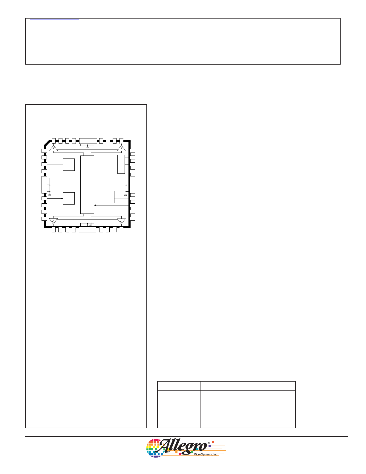
(PLCC)
1A
OUT
65
NC
7
NC
8
PFD
9
RC
10
1
GND
11
GND
12
GND
13
REF
14
RC
2
15
LOGIC
16
V
SUPPLY
DD
NC NC
17 29
18
2A
OUT
1
HOME
DIR
SENSE
4321
PWM
TIMER
÷8
2019
221
MS
MS
SENSE
GND
GND
ABSOLUTE MAXIMUM RATINGS
at TA = +25°C
Load Supply Voltage, VBB............. 35 V
Output Current, I
Logic Supply Voltage, VDD........... 7.0 V
Logic Input Voltage Range, V
(tw >30 ns)..... -0.3 V to VDD + 0.3 V
(tw <30 ns)........... -1 V to VDD + 1 V
Sense Voltage, V
Reference Voltage, V
Package Power Dissipation,
PD................................. See page 3
Operating Temperature Range, T
(A3977Kx) ............ -40°C to +125°C
(A3977Sx) .............. -20°C to +85°C
Junction Temperature, TJ......... +150°C
Storage Temperature Range,
TS......................... -55°C to +150°C
* Output current rating may be limited by
duty cycle, ambient temperature, and heat
sinking. Under any set of conditions, do not
exceed the specified current rating or a
junction temperature of 150°C.
OUT
SENSE
1
LOAD
GND
GND
SUPPLY
44 43 424140
V
BB1
TRANSLATOR
& CONTROL LOGIC
V
BB2
232221
2
GND
GND
LOAD
SUPPLY
REG
SLEEP
SR
ENABLE
RESET
1B
OUT
CHARGE PUMP
2827262524
2B
OUT
Dwg. PP-075-1
39
38
37
36
35
34
33
32
31
30
.................. ±2.5 A
IN
................. 0.5 V
................ V
REF
A
DD
NC
CP
CP
V
GND
GND
GND
V
STEP
NC
The A3977xED and A3977xLP are complete microstepping motor drivers
with built-in translator. They are designed to operate bipolar stepper motors in
full-, half-, quarter-, and eighth-step modes, with output drive capability of 35
V and ±2.5 A. The A3977 includes a fixed off-time current regulator that has
the ability to operate in slow-, fast-, or mixed-decay modes. This currentdecay control scheme results in reduced audible motor noise, increased step
accuracy, and reduced power dissipation.
2
1
CP
The translator is the key to the easy implementation of the A3977. By
simply inputting one pulse on the STEP input the motor will take one step
(full, half, quarter, or eighth depending on two logic inputs). There are no
phase-sequence tables, high-frequency control lines, or complex interfaces to
program. The A3977 interface is an ideal fit for applications where a complex
REG
µP is unavailable or over-burdened.
Internal synchronous-rectification control circuitry is provided to improve
power dissipation during PWM operation.
Internal circuit protection includes thermal shutdown with hysteresis,
under-voltage lockout (UVLO) and crossover-current protection. Special
power-up sequencing is not required.
The A3977 is supplied in a choice of two power packages, a 44-pin
plastic PLCC with copper batwing tabs (suffix ED), and a thin (<1.2 mm), 28pin TSSOP with an exposed thermal pad (suffix LP). The SLP package is
available in a lead-free version (100% matte tin leadframe).
FEATURES
*
■ ±2.5 A, 35 V Output Rating
■ Low r
Outputs, 0.45 Ω Source, 0.36 Ω Sink Typical
DS(on)
■ Automatic Current Decay Mode Detection/Selection
■ 3.0 V to 5.5 V Logic Supply Voltage Range
■ Mixed, Fast, and Slow Current Decay Modes
■ Home Output
■ Synchronous Rectification for Low Power Dissipation
■ Internal UVLO and Thermal Shutdown Circuitry
■ Crossover-Current Protection
Always order by complete part number:
Part Number Package
A3977KED 44-pin PLCC
A3977KLP 28-pin TSSOP
A3977SED 44-pin PLCC
A3977SED-T 44-pin PLCC; Lead-free
A3977SLP 28-pin TSSOP
A3977SLP-T 28-pin TSSOP; Lead-free
Page 2
3977
MICROSTEPPING DMOS DRIVER
WITH TRANSLATOR
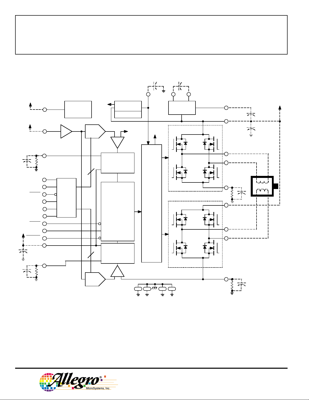
FUNCTIONAL BLOCK DIAGRAM
LOGIC
SUPPLY
REF.
SUPPLY
V
REF
RC
DD
1
UVLO
AND
FA
LT
DA
2 V
PWM LATCH
BLANKING
MIXED DECAY
REGULATOR
BANDGAP
SENSE
+-
CP
V
REG
2
CHARGE
CP
1
V
CP
LOAD
SUPPLY
PUMP
BB1
V
1
V
CP
DMOS H BRIDGE
OUT
OUT
1A
1B
V
PFD
STEP
DIR
RESET
MS
MS
HOME
SLEEP
SR
ENABLE
1
2
PFD
RC
4
TRANSLATOR
PWM TIMER
DMOS H BRIDGE
SENSE
V
BB2
1
GATE DRIVE
OUT
OUT
2A
2B
CONTROL LOGIC
PWM TIMER
PWM LATCH
BLANKING
MIXED DECAY
2
DAC
+-
SENSE
2
Dwg. FP-050-2
2
115 Northeast Cutoff, Box 15036
Worcester, Massachusetts 01615-0036 (508) 853-5000
Copyright © 2002, 2003 Allegro MicroSystems, Inc.
Page 3
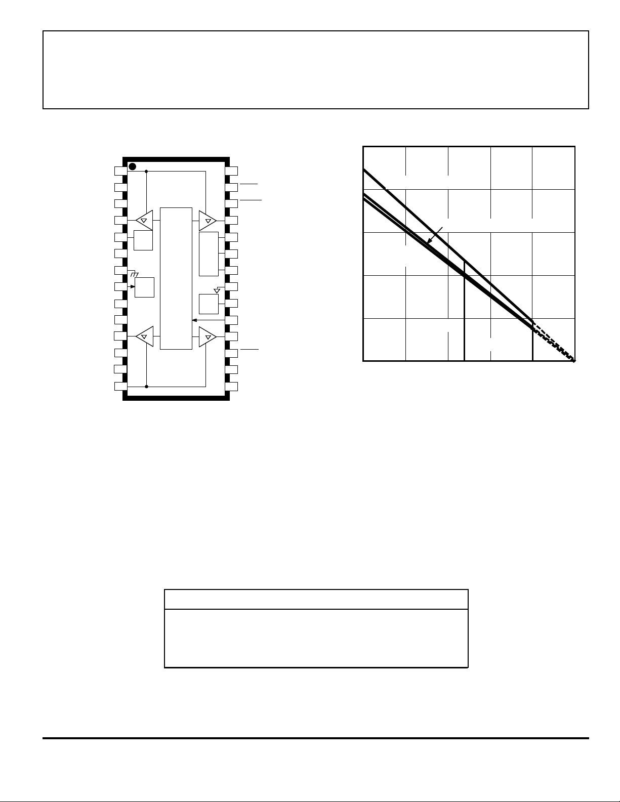
A3977xLP
(TSSOP)
3977
MICROSTEPPING DMOS DRIVER
WITH TRANSLATOR
5.0
SENSE
SUPPLY
SENSE
1
1
HOME
2
3
DIR
1A
OUT
4
PFD
5
PWM
1
RC
AGND
REF
2
RC
LOGIC
10
2A
OUT
11
MS
2
12
MS
1
13
2
14 15
TIMER
6
7
8
÷8
9
V
DD
TRANSLATOR
& CONTROL LOGIC
REG
LOAD
V
BB1
28
SUPPLY
SLEEP
27
26
ENABLE
OUT
25
CP
24
CP
23
V
22
CHARGE PUMP
PGND
21
V
20
STEP
19
18
OUT
RESET
17
16
SR
LOAD
V
BB2
SUPPLY
Dwg. PP-075
CP
REG
1
SUFFIX '–LP', RθJA = 28°C/W*
4.0
1B
2
1
3.0
SUFFIX '–LP',
θJA = 33°C/W†
R
SUFFIX '–ED', RθJA = 32°C/W†
2.0
1.0
2B
0
ALLOWABLE PACKAGE POWER DISSIPATION IN WATTS
25
2
Package Thermal Resistance, R
A3977xLP ......................... 28°C/W
A3977xED ........................ 32°C/W
A3977xLP ......................... 33°C/W
SUFFIX 'S–'
SUFFIX 'K–'
50 75 100 125 150
AMBIENT TEMPERATURE IN °°°°C
Dwg. GP-018-2A
θJA
*
†
†
* Measured on JEDEC standard “High-K” four-layer board.
† Measured on typical two-sided PCB with three square inches
2
(1935 mm
) copper ground area.
www.allegromicro.com
Table 1. Microstep Resolution Truth Table
MS
1
MS
2
Resolution
L L Full step (2 phase)
H L Half step
L H Quarter step
H H Eighth step
3
Page 4
3977
MICROSTEPPING DMOS DRIVER
WITH TRANSLATOR
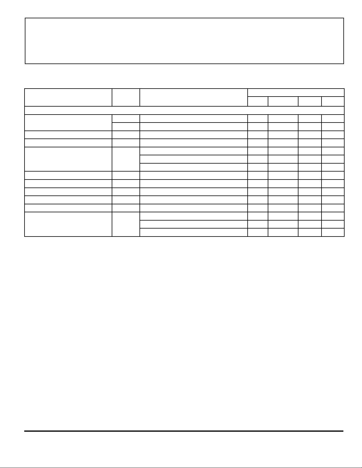
ELECTRICAL CHARACTERISTICS at T
= +25°C, V
A
= 35 V, VDD = 3.0 V to 5.5V (unless otherwise
BB
noted)
Limits
Characteristic Symbol Test Conditions Min. Typ. Max. Units
Output Drivers
Load Supply Voltage Range V
BB
Operating 8.0 – 35 V
During sleep mode 0 – 35 V
Output Leakage Current I
Output On Resistance r
DS(on)
Body Diode Forward Voltage V
DSS
V
= V
OUT
V
OUT
Source driver, I
Sink driver, I
Source diode, IF = -2.5 A – – 1.4 V
F
BB
= 0 V – <1.0 -20 µA
= -2.5 A
OUT
= 2.5 A – 0.36 0.43 Ω
OUT
– <1.0 20 µA
– 0.45 0.57 Ω
Sink diode, IF = 2.5 A – – 1.4 V
Motor Supply Current I
BB
f
< 50 kHz – – 8.0 mA
PWM
Control Logic
Logic Supply Voltage Range V
Logic Input Voltage V
V
Logic Input Current I
I
Maximum STEP Frequency f
HOME Output Voltage V
Blank Time t
BLANK
Fixed Off Time t
DD
IN(1)
IN(0)
IN(1)
IN(0)
STEP
OH
V
OL
off
Operating, outputs disabled
– – 6.0 mA
Sleep mode – – 20 µA
Operating 3.0 5.0 5.5 V
VIN = 0.7V
VIN = 0.3V
DD
DD
0.7V
DD
– – 0.3V
-20 <1.0 20 µA
-20 <1.0 20 µA
––V
DD
V
500* – – kHz
I
= -200 µA 0.7V
OH
I
= 200 µA – – 0.3V
OL
R
= 56 kΩ, C
t
R
= 56 kΩ, Ct = 680 pF 30 38 46 µs
t
= 680 pF 700 950 1200 ns
t
DD
– – V
DD
V
continued next page …
4
115 Northeast Cutoff, Box 15036
Worcester, Massachusetts 01615-0036 (508) 853-5000
Page 5
3977
MICROSTEPPPING DMOS DRIVER
WITH TRANSLATOR
ELECTRICAL CHARACTERISTICS at TA = +25°C, VBB = 35 V, VDD = 3.0 V to 5.5V (unless otherwise
noted)
Limits
Characteristic Symbol Test Conditions
Control Logic (cont’d)
Mixed Decay Trip Point PFDH – 0.6V
PFDL – 0.21V
Ref. Input Voltage Range V
Reference Input Current I
Gain (Gm) Error
E
(note 3)
Crossover Dead Time t
Thermal Shutdown Temp. T
Thermal Shutdown Hysteresis ∆T
UVLO Enable Threshold V
UVLO
UVLO Hysteresis ∆V
Logic Supply Current I
Operating 0 – V
REF
REF
V
G
DT
J
J
UVLO
DDfPWM
= 2 V, Phase Current = 38.27% – – ±10 %
REF
V
= 2 V, Phase Current = 70.71% – – ±5.0 %
REF
= 2 V, Phase Current = 100.00% – – ±5.0 %
V
REF
SR enabled 100 475 800 ns
Increasing V
DD
< 50 kHz – – 12 mA
Outputs off – – 10 mA
Sleep mode – – 20 µA
* Operation at a step frequency greater than the specifi ed minimum value is possible but not warranteed.
NOTES: 1. Typical Data is for design information only.
2. Negative current is defi ned as coming out of (sourcing) the specifi ed device terminal.
3. EG = ([V
REF
/8] – V
SENSE
)/(V
REF
/8)
Min. Typ. Max. Units
DD
DD
–V
–V
DD
– 0 ±3.0 µA
– 165 – °C
–15 –°C
2.45 2.7 2.95 V
0.05 0.10 – V
V
www.allegromicro.com
5
Page 6

3977
MICROSTEPPING DMOS DRIVER
WITH TRANSLATOR
Functional Description
Device Operation. The A3977 is a complete
microstepping motor driver with built in translator for
easy operation with minimal control lines. It is designed
to operate bipolar stepper motors in full-, half-, quarterand eighth-step modes. The current in each of the two
output H-bridges, all n-channel DMOS, is regulated with
fixed off time pulse-width modulated (PWM) control
circuitry. The H-bridge current at each step is set by the
value of an external current sense resistor (R
voltage (V
), and the DAC’s output voltage controlled
REF
), a reference
S
by the output of the translator.
At power up, or reset, the translator sets the DACs and
phase current polarity to initial home state (see figures for
home-state conditions), and sets the current regulator for
both phases to mixed-decay mode. When a step command
signal occurs on the STEP input the translator automatically sequences the DACs to the next level (see table 2 for
the current level sequence and current polarity). The
microstep resolution is set by inputs MS
and MS2 as
1
shown in table 1. If the new DAC output level is lower
than the previous level the decay mode for that H-bridge
will be set by the PFD input (fast, slow or mixed decay).
If the new DAC level is higher or equal to the previous
level then the decay mode for that H-bridge will be slow
decay. This automatic current-decay selection will
improve microstepping performance by reducing the
distortion of the current waveform due to the motor
BEMF.
Reset Input (RESET). The RESET input (active low)
sets the translator to a predefined home state (see figures
for home state conditions) and turns off all of the DMOS
outputs. The HOME output goes low and all STEP inputs
are ignored until the RESET input goes high.
Home Output (HOME). The HOME output is a logic
output indicator of the initial state of the translator. At
power up the translator is reset to the home state (see
figures for home state conditions).
Step Input (STEP). A low-to-high transition on the
STEP input sequences the translator and advances the
motor one increment. The translator controls the input to
the DACs and the direction of current flow in each winding. The size of the increment is determined by the state
of inputs MS
Microstep Select (MS
and MS2 (see table 1).
1
and MS2). Input terminals
1
MS1 and MS2 select the microstepping format per
table 1. Changes to these inputs do not take effect until
the STEP command (see figure).
Direction Input (DIR). The state of the DIRECTION
input will determine the direction of rotation of the motor.
Internal PWM Current Control. Each H-bridge is
controlled by a fixed off time PWM current-control circuit
that limits the load current to a desired value (I
TRIP
).
Initially, a diagonal pair of source and sink DMOS outputs
are enabled and current flows through the motor winding
and RS. When the voltage across the current-sense resistor
equals the DAC output voltage, the current-sense comparator resets the PWM latch, which turns off the source
driver (slow-decay mode) or the sink and source drivers
(fast- or mixed-decay modes).
The maximum value of current limiting is set by the
selection of R
and the voltage at the V
S
input with a
REF
transconductance function approximated by:
max = V
I
TRIP
The DAC output reduces the V
REF
/8R
REF
S
output to the
current-sense comparator in precise steps (see table 2 for
% I
max at each step).
TRIP
= (% I
I
TRIP
max/100) x I
TRIP
TRIP
max
It is critical to ensure that the maximum rating (0.5 V)
on the SENSE terminal is not exceeded. For full-step
mode, V
VDD, because the peak sense value is 0.707 x V
all other modes V
can be applied up to the maximum rating of
REF
REF
should not exceed 4 V.
REF
/8. In
6
115 Northeast Cutoff, Box 15036
Worcester, Massachusetts 01615-0036 (508) 853-5000
Page 7

MICROSTEPPING DMOS DRIVER
Functional Description (cont’d)
3977
WITH TRANSLATOR
Fixed Off-Time. The internal PWM current-control
circuitry uses a one shot to control the time the driver(s)
remain(s) off. The one shot off-time, t
the selection of an external resistor (R
(C
) connected from the RC timing terminal to ground.
T
, is determined by
off
) and capacitor
T
The off time, over a range of values of CT = 470 pF to
1500 pF and RT = 12 kΩ to 100 kΩ is approximated by:
= RTC
t
off
T
RC Blanking. In addition to the fixed off time of the
PWM control circuit, the C
component sets the compara-
T
tor blanking time. This function blanks the output of the
current-sense comparator when the outputs are switched
by the internal current-control circuitry. The comparator
output is blanked to prevent false over-current detection
due to reverse recovery currents of the clamp diodes, and/
or switching transients related to the capacitance of the
load. The blank time t
t
BLANK
can be approximated by:
BLANK
= 1400C
T
Charge Pump. (CP1 and CP2). The charge pump is
used to generate a gate supply greater than VBB to drive
the source-side DMOS gates. A 0.22 µF ceramic capaci-
tor should be connected between CP1 and CP2 for pumping purposes. A 0.22 µF ceramic capacitor is required
between VCP and VBB to act as a reservoir to operate the
high-side DMOS devices.
. This internally generated voltage is used to operate
V
REG
the sink-side DMOS outputs. The V
be decoupled with a 0.22 µF capacitor to ground. V
terminal should
REG
REG
is
internally monitored and in the case of a fault condition,
the outputs of the device are disabled.
Enable Input (ENABLE). This active-low input
enables all of the DMOS outputs. When logic high the
outputs are disabled. Inputs to the translator (STEP,
DIRECTION, MS
, MS2) are all active independent of the
1
ENABLE input state.
Shutdown. In the event of a fault (excessive junction
temperature, or low voltage on V
) the outputs of the
CP
device are disabled until the fault condition is removed.
At power up, and in the event of low VDD, the undervoltage lockout (UVLO) circuit disables the drivers and
resets the translator to the HOME state.
Sleep Mode (SLEEP). An active-low control input
used to minimize power consumption when not in use.
This disables much of the internal circuitry including the
output DMOS, regulator, and charge pump. A logic high
allows normal operation and startup of the device in the
home position. When coming out of sleep mode, wait
1 ms before issuing a STEP command to allow the charge
pump (gate drive) to stabilize.
Percent Fast Decay Input (PFD). When a STEP
input signal commands a lower output current from the
previous step, it switches the output current decay to either
slow-, fast-, or mixed-decay depending on the voltage
level at the PFD input. If the voltage at the PFD input is
greater than 0.6V
then slow-decay mode is selected. If
DD
the voltage on the PFD input is less than 0.21VDD then
fast-decay mode is selected. Mixed decay is between
these two levels. This terminal should be decoupled with
a 0.1 µF capacitor.
Mixed Decay Operation. If the voltage on the PFD
input is between 0.6V
and 0.21VDD, the bridge will
DD
operate in mixed-decay mode depending on the step
sequence (see figures). As the trip point is reached, the
device will go into fast-decay mode until the voltage on
the RC terminal decays to the voltage applied to the PFD
terminal. The time that the device operates in fast decay is
approximated by:
= RTCTIn (0.6VDD/V
t
FD
After this fast decay portion, t
, the device will
FD
PFD
)
switch to slow-decay mode for the remainder of the fixed
off-time period.
www.allegromicro.com
7
Page 8

3977
MICROSTEPPING DMOS DRIVER
WITH TRANSLATOR
Functional Description (cont’d)
Synchronous Rectification. When a PWM off cycle
is triggered by an internal fixed off-time cycle, load
current will recirculate according to the decay mode
selected by the control logic. The A3977 synchronous
rectification feature will turn on the appropriate
MOSFETs during the current decay and effectively short
out the body diodes with the low r
driver. This will
DS(on)
reduce power dissipation significantly and eliminate the
need for external Schottky diodes for most applications.
The synchronous rectification can be set in either
active mode or disabled mode.
Timing Requirements
(T
A
STEP
= +25°C, V
= 5 V, Logic Levels are VDD and Ground)
DD
50%
B
A
Active Mode. When the SR input is logic low, active
mode is enabled and synchronous rectification will occur.
This mode prevents reversal of the load current by turning
off synchronous rectification when a zero current level is
detected. This prevents the motor winding from conducting in the reverse direction.
Disabled Mode. When the SR input is logic high,
synchronous rectification is disabled. This mode is
typically used when external diodes are required to
transfer power dissipation from the A3977 package to the
external diodes.
C D
MS1/MS2/
DIR/RESET
E
SLEEP
Dwg. WP-042
A. Minimum Command Active Time
Before Step Pulse (Data Set-Up Time) ..... 200 ns
B. Minimum Command Active Time
After Step Pulse (Data Hold Time)............ 200 ns
C. Minimum STEP Pulse Width ...................... 1.0 µs
D. Minimum STEP Low Time ......................... 1.0 µs
E. Maximum Wake-Up Time ......................... 1.0 ms
8
115 Northeast Cutoff, Box 15036
Worcester, Massachusetts 01615-0036 (508) 853-5000
Page 9

MICROSTEPPING DMOS DRIVER
Applications Information
3977
WITH TRANSLATOR
Layout.
The printed wiring board should use a heavy ground
plane.
For optimum electrical and thermal performance, the
driver should be soldered directly onto the board.
The load supply terminal, V
, should be decoupled
BB
with an electrolytic capacitor (>47 µF is recommended)
placed as close to the device as possible.
To avoid problems due to capacitive coupling of the
high dv/dt switching transients, route the bridge-output
traces away from the sensitive logic-input traces. Always
drive the logic inputs with a low source impedance to
increase noise immunity.
Grounding. A star ground system located close to the
driver is recommended.
The 44-lead PLCC has the analog ground and the
power ground internally bonded to the power tabs of the
package (leads 44, 1, 2, 11 – 13, 22 – 24, and 33 – 35).
On the 28-lead TSSOP package, the analog ground
(lead 7) and the power ground (lead 21) must be connected together externally. The copper ground plane
located under the exposed thermal pad is typically used as
the star ground.
Current Sensing. To minimize inaccuracies caused by
ground-trace IR drops in sensing the output current level,
the current-sense resistor (R
) should have an independent
S
ground return to the star ground of the device. This path
should be as short as possible. For low-value sense
resistors the IR drops in the printed wiring board sense
resistor’s traces can be significant and should be taken
into account. The use of sockets should be avoided as
they can introduce variation in RS due to their contact
resistance.
Allegro MicroSystems recommends a value of R
S
given by
= 0.5/I
R
S
TRIP
max
Thermal Protection. Circuitry turns off all drivers
when the junction temperature reaches 165°C, typically.
It is intended only to protect the device from failures due
to excessive junction temperatures and should not imply
that output short circuits are permitted. Thermal shutdown has a hysteresis of approximately 15°C.
www.allegromicro.com
9
Page 10

3977
MICROSTEPPPING DMOS DRIVER
WITH TRANSLATOR
Table 2. Step Sequencing
Home State = 45º Step Angle, DIR = H
Phase 1 Current
Full Step Half Step ¼ Step ⅛ Step
1 1 1 100.00 0.00 0.0
2 98.08 19.51 11.3
2 3 92.39 38.27 22.5
4 83.15 55.56 33.8
1 2 3 5 70.71 70.71 45.0
6 55.56 83.15 56.3
4 7 38.27 92.39 67.5
8 19.51 98.08 78.8
3 5 9 0.00 100.00 90.0
10 –19.51 98.08 101.3
6 11 –38.27 92.39 112.5
12 –55.56 83.15 123.8
2 4 7 13 –70.71 70.71 135.0
14 –83.15 55.56 146.3
8 15 –92.39 38.27 157.5
16 –98.08 19.51 168.8
5 9 17 –100.00 0.00 180.0
18 –98.08 –19.51 191.3
10 19 –92.39 –38.27 202.5
20 –83.15 –55.56 213.8
3 6 11 21 –70.71 –70.71 225.0
22 –55.56 –83.15 236.3
12 23 –38.27 –92.39 247.5
24 –19.51 –98.08 258.8
7 13 25 0.00 –100.00 270.0
26 19.51 –98.08 281.3
14 27 38.27 –92.39 292.5
28 55.56 –83.15 303.8
4 8 15 29 70.71 –70.71 315.0
30 83.15 –55.56 326.3
16 31 92.39 –38.27 337.5
32 98.08 –19.51 348.8
(%I
trip
(%)
max)
Phase 2 Current
(%I
max)
trip
(%)
Step Angle
(º)
10
115 Northeast Cutoff, Box 15036
Worcester, Massachusetts 01615-0036 (508) 853-5000
Page 11

STEP
INPUT
HOME
OUTPUT
70.7%
3977
MICROSTEPPING DMOS DRIVER
WITH TRANSLATOR
Full-Step Operation
MS1 = MS2 = L, DIR = H
SLOW
DECAY
PHASE 1
CURRENT
–70.7%
70.7%
PHASE 2
CURRENT
–70.7%
SLOW
DECAY
Dwg. WK-004-15
www.allegromicro.com
The vector addition of the output currents at any step is
100%.
11
Page 12

3977
MICROSTEPPING DMOS DRIVER
WITH TRANSLATOR
Half-Step Operation
= H, MS2 = L, DIR = H
MS
1
STEP
INPUT
HOME
OUTPUT
100%
70.7%
PHASE 1
CURRENT
–70.7%
–100%
100%
70.7%
PHASE 2
CURRENT
70.7%
–100%
SLOW
DECAY
MIXED
DECAY
MIXED
DECAY
SLOW
DECAY
SLOW
DECAY
MIXED
DECAY
MIXED
DECAY
SLOW
DECAY
SLOW
DECAY
MIXED
DECAY
MIXED
DECAY
SLOW
DECAY
DECAY
DECAY
MIXED
SLOW
SLOW
MIXED
Dwg. WK-004-14
DECAY
DECAY
12
The mixed-decay mode is controlled by the percent fast
decay voltage (V
). If the voltage at the PFD input is
PFD
greater than 0.6VDD then slow-decay mode is selected. If
the voltage on the PFD input is less than 0.21VDD then
fast-decay mode is selected. Mixed decay is between
these two levels.
115 Northeast Cutoff, Box 15036
Worcester, Massachusetts 01615-0036 (508) 853-5000
Page 13

STEP
INPUT
HOME
OUTPUT
MICROSTEPPING DMOS DRIVER
Quarter-Step Operation
MS
= L, MS2 = H, DIR = H
1
3977
WITH TRANSLATOR
100%
70.7%
38.3%
PHASE 1
CURRENT
–38.3%
–70.7%
–100%
100%
70.7%
38.3%
PHASE 2
CURRENT
–38.3%
–70.7%
–100%
SLOW
DECAY
MIXED
DECAY
MIXED
DECAY
SLOW
DECAY
SLOW
DECAY
MIXED
DECAY
MIXED
DECAY
SLOW
DECAY
Dwg. WK-004-13
www.allegromicro.com
The mixed-decay mode is controlled by the percent fast
decay voltage (V
). If the voltage at the PFD input is
PFD
greater than 0.6VDD then slow-decay mode is selected. If
the voltage on the PFD input is less than 0.21VDD then
fast-decay mode is selected. Mixed decay is between
these two levels.
13
Page 14

3977
MICROSTEPPING DMOS DRIVER
WITH TRANSLATOR
8 Microstep/Step Operation
MS
= MS2 = H, DIR = H
1
STEP
INPUT
HOME
OUTPUT
100%
70.7%
38.3%
PHASE 1
CURRENT
–38.3%
–70.7%
–100%
100%
70.7%
38.3%
PHASE 2
CURRENT
–38.3%
–70.7%
–100%
SLOW
DECAY
MIXED
DECAY
MIXED
DECAY
SLOW
DECAY
SLOW
DECAY
MIXED
DECAY
MIXED
DECAY
SLOW
DECAY
Dwg. WK-004-12
14
The mixed-decay mode is controlled by the percent fast
decay voltage (V
). If the voltage at the PFD input is
PFD
greater than 0.6VDD then slow-decay mode is selected. If
the voltage on the PFD input is less than 0.21VDD then
fast-decay mode is selected. Mixed decay is between
these two levels.
115 Northeast Cutoff, Box 15036
Worcester, Massachusetts 01615-0036 (508) 853-5000
Page 15

3977
MICROSTEPPING DMOS DRIVER
WITH TRANSLATOR
Terminal List
Terminal A3977xLP A3977xED
Name Terminal Description (TSSOP) (PLCC)
GND Analog and power ground – 44, 1, 2
SENSE
HOME Logic output 2 4
DIR Logic Input 3 5
OUT
NC No (internal) connection – 7, 8
PFD Mixed decay setting 5 9
RC1 Analog Input for fixed offtime – bridge 1 6 10
GND Analog and power ground – 11, 12, 13
AGND Analog ground 7* –
REF Gm reference input 8 14
RC2 Analog input for fixed offtime – bridge 2 9 15
LOGIC SUPPLY VDD, the logic supply voltage 10 16
NC No (internal) connection – 17
OUT2A DMOS H bridge 2 output A 11 18
MS2 Logic input 12 19
MS1 Logic input 13 20
SENSE2 Sense resistor for bridge 2 14 21
GND Analog and power ground – 22, 23, 24
LOAD SUPPLY2 VBB2, the load supply for bridge 2 15 25
SR Logic input 16 26
RESET Logic input 17 27
OUT2B DMOS H bridge 2 output B 18 28
NC No (internal) connection – 29, 30
STEP Logic input 19 31
VREG Regulator decoupling 20 32
PGND Power ground 21* –
GND Analog and power ground – 33, 34, 35
VCP Reservoir capacitor 22 36
CP1 Charge pump capacitor 23 37
CP2 Charge pump capacitor 24 38
NC No (internal) connection – 39
OUT1B DMOS H bridge 1 output B 25 40
ENABLE Logic input 26 41
SLEEP Logic input 27 42
LOAD SUPPLY1 VBB1, the load supply for bridge 1 28 43
1 Sense resistor for bridge 1 1 3
1A DMOS H bridge 1 output A 4 6
* AGND and PGND on the TSSOP package must be connected together externally.
www.allegromicro.com
15
Page 16

3977
MICROSTEPPING DMOS DRIVER
WITH TRANSLATOR
A3977xED
0.319
0.291
0.319
0.291
0.021
0.013
0.050
BSC
0.020
MIN
0.180
0.165
0.695
0.685
0.656
0.650
0.032
0.026
28
29
18
17
Dimensions in Inches
(controlling dimensions)
INDEX AREA
39
144
40
0.656
0.650
28
2
0.695
0.685
6
18
7
Dwg. MA-005-44A in
29
17.65
17.40
16.662
16.510
0.812
0.661
INDEX AREA
39
144
17.65
17.40
2
40
16.662
16.510
8.10
7.39
8.10
7.39
0.533
0.331
1.27
BSC
0.51
MIN
4.57
4.20
NOTES: 1. Exact body and lead configuration at vendor’s option within limits shown.
2. Lead spacing tolerance is non-cumulative.
3. Webbed lead frame. Terminals 1, 2, 11, 12, 13, 22, 23, 24, 33, 34, 35, and 44 are internally one piece.
4. Supplied in standard sticks/tubes of 27 devices or add “TR” to part number for tape and reel.
17
Dimensions in Millimeters
(for reference only)
7
6
Dwg. MA-005-44A mm
16
115 Northeast Cutoff, Box 15036
Worcester, Massachusetts 01615-0036 (508) 853-5000
Page 17

3977
MICROSTEPPING DMOS DRIVER
WITH TRANSLATOR
0.177
0.169
0.012
0.0075
0.0472
MAX
INDEX
AREA
3
0.197
0.386
0.378
5.0
0.118
28 15
1 2
0.0059
0.00
28 15
A3977xLP
GAUGE PLANE
SEATING PLANE
0.026
BSC
0.0079
0.0035
0.0098
BSC
0° TO 8°
EXPOSED
THERMAL PAD
0.0394
0.260
0.244
REF
Dwg. MA-008-30A in
0.030
0.018
Dimensions in Inches
(for reference only)
4.50
4.30
0.30
0.19
1.20
MAX
1 2
0.15
0.00
INDEX
AREA
3
9.80
9.60
3.0
GAUGE PLANE
SEATING PLANE
0.65
BSC
0.20
0.09
0.25
BSC
0° TO 8°
EXPOSED
THERMAL PAD
NOTES: 1. Exact body and lead configuration at vendor’s option within limits shown.
2. Lead spacing tolerance is non-cumulative.
3. Supplied in standard sticks/tubes of 49 devices or add “TR” to part number for tape and reel.
6.60
6.20
1.00
REF
Dwg. MA-008-30A mm
0.75
0.45
Dimensions in Millimeters
(controlling dimensions)
www.allegromicro.com
17
Page 18

3977
MICROSTEPPING DMOS DRIVER
WITH TRANSLATOR
18
The products described here are manufactured under one or more
U.S. patents or U.S. patents pending.
Allegro MicroSystems, Inc. reserves the right to make, from time to
time, such departures from the detail specifications as may be
required to permit improvements in the performance, reliability, or
manufacturability of its products. Before placing an order, the user is
cautioned to verify that the information being relied upon is current.
Allegro products are not authorized for use as critical components
in life-support devices or systems without express written approval.
The information included herein is believed to be accurate and
reliable. However, Allegro MicroSystems, Inc. assumes no responsibility for its use; nor for any infringement of patents or other rights of
third parties which may result from its use.
115 Northeast Cutoff, Box 15036
Worcester, Massachusetts 01615-0036 (508) 853-5000
 Loading...