

Page 1
查询3973供应商
Data Sheet
29319.34
3973
PRELIMINARY INFORMATION
(Subject to change without notice)
December 1, 2000
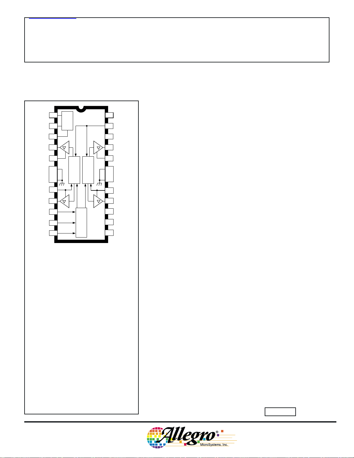
D
24
23
22
21
20
19
18
17
16
15
14
13
Dwg. PP-069-3
+ 0.3 V
DD
OSC
SLEEP
V
REG
OUT
2B
LOAD
SUPPLY
GROUND
GROUND
SENSE
OUT
2A
LOGIC
SUPPLY
MUX
REF
2
2
VCP
1
V
BB1
PUMP
CHARGE
6-BIT DAC
& LOGIC
& LOGIC
6-BIT DAC
SERIAL PORT
V
BB2
DD
V
CP1
CP2
OUT
LOAD
SUPPLY
GROUND
GROUND
SENSE
OUT
STROBE
CLOCK
DATA
2
3
1B
4
5
1
6
7
1
8
9
1A
9
10
11
12
ABSOLUTE MAXIMUM RATINGS
= +25°C
at T
A
Load Supply Voltage, VBB................ 35 V
Output Current, I
Logic Supply Voltage, VDD.............. 7.0 V
Logic Input Voltage Range,
VIN................ -0.3 V to V
Reference Voltage, V
Sense Voltage (dc), VS................ 500 mV
Package Power Dissipation, P
A3973SB ............................... 3.1 W
A3973SLB ............................ 2.2 W
Operating Temperature Range,
TA.......................... -20°C to +85°C
Junction Temperature, TJ............. +150°C
Storage Temperature Range,
TS......................... -55°C to +150°C
Output current rating may be limited by duty
cycle, ambient temperature, and heat sinking.
Under any set of conditions, do not exceed the
specified current rating or a junction temperature of 150°C.
...................... ±1.0 A
OUT
..................... 3 V
REF
DUAL DMOS FULL-BRIDGE MICRO-
STEPPING PWM MOTOR DRIVER
Designed for pulse-width modulated (PWM) current control of
bipolar microstepping stepper motors, the A3973SB and A3973SLB are
capable of continuous output currents to ±1 A and operating voltages to
35 V. Internal fixed off-time PWM current-control timing circuitry can
be programmed via a serial interface to operate in slow, fast, and mixed
current-decay modes. The A3973SB (DIP) and the A3973SLB (SOIC)
are electrically identical and differ only in package style.
The desired load-current level is set via the serial port with two 6-bit
linear DACs in conjunction with a reference voltage. The six bits of
control allow maximum flexibility in torque control for a variety of step
methods, from microstepping to full-step drive. Load current is set in
1.56% increments of the maximum value.
Synchronous rectification circuitry allows the load current to flow
r
through the low
decay. This feature will eliminate the need for external clamp diodes in
most applications, saving cost and external component count, while
minimizing power dissipation.
Internal circuit protection includes thermal shutdown with hysteresis, transient-suppression diodes, and crossover-current protection.
Special power-up sequencing is not required.
The A3973SB is supplied in a 24-lead plastic DIP with a copper
batwing power tab; the A3973SLB is supplied in a 24-lead plastic SOIC
with a copper batwing power tab for surface-mount applications. The
power tabs are at ground potential and need no electrical isolation.
FEATURES
■ ±1 A, 35 V Continuous Output Rating
■ Low r
■ Optimized Microstepping via 6-Bit Linear DACs
■ Programmable Mixed, Fast, and Slow Current-Decay Modes
■ 4 MHz Internal Oscillator for Digital Timing
■ Serial-Interface Controls Chip Functions
■ Synchronous Rectification for Low Power Dissipation
■ Internal UVLO and Thermal Shutdown Circuitry
■ Crossover-Current Protection
■ Precision 2 V Reference
■ Inputs Compatible with 3.3 V or 5 V Control Signals
■ Sleep and Idle Modes
Always order by complete part number, e.g., A3973SB .
DMOS Output Drivers
DS(on)
of the DMOS output driver during the current
DS(on)
Page 2
3973
DUAL DMOS FULL-BRIDGE
MICROSTEPPING PWM MOTOR DRIVER
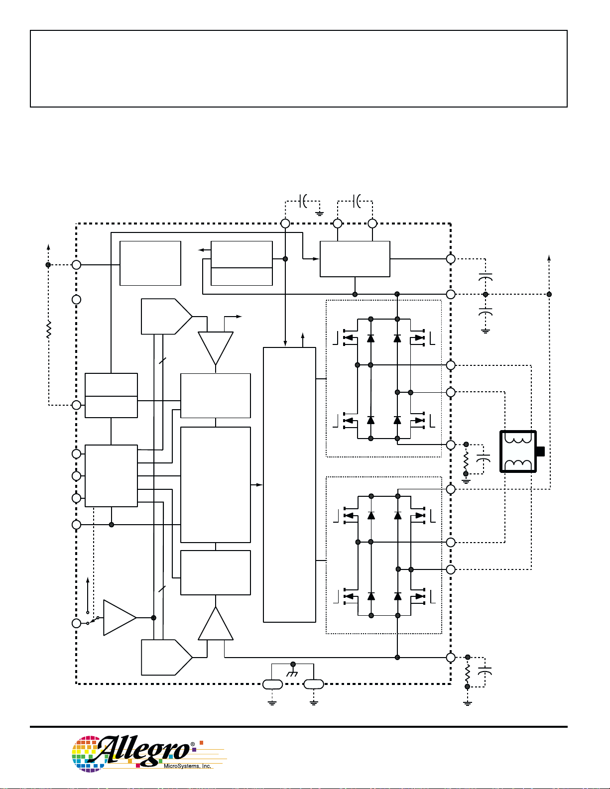
FUNCTIONAL BLOCK DIAGRAM
LOGIC
SUPPLY
CLOCK
DATA
STROBE
SLEEP
V
MUX
OSC
15
DD
14
24
11
12
10
23
OSCILATOR
OSC SELECT/
DIVIDER
SERIAL
PORT
2 V
UVLO AND
FAULT
DETECT
6-BIT
LINEAR
DAC
6
6
2 V
REGULATOR
BANDGAP
+-
PROGRAMMABLE
PWM TIMER
FIXED-OFF
BLANK
MIXED DECAY
CONTROL
LOGIC
PHASE 1/2
SYNC. RECT. MODE
SYNC. RECT. DISABLE
MODE 1/2
PROGRAMMABLE
PWM TIMER
FIXED-OFF
BLANK
MIXED DECAY
SENSE
1
V
22
GATE
DRIVE
0.22 µF
REG
V
CP
0.22 µF
3
CP1CP2
2
CHARGE PUMP
DMOS H-BRIDGE
DMOS H-BRIDGE
1
5
9
4
8
20
16
21
V
CP
V
BB1
OUT
1A
OUT
1B
SENSE
V
BB2
OUT
2A
OUT
2B
1
0.1 µF
0.22 µF
LOAD
SUPPLY
2
REF
13
Dwg. FP-050-1
BUFFER
6-BIT
LINEAR
DAC
+-
GROUND
6
18
7
19
115 Northeast Cutoff, Box 15036
Worcester, Massachusetts 01615-0036 (508) 853-5000
Copyright © 2000, Allegro MicroSystems, Inc.
17
SENSE
2
0.1
µ
F
Page 3

3973
DUAL DMOS FULL-BRIDGE
MICROSTEPPING PWM MOTOR DRIVER
ELECTRICAL CHARACTERISTICS at TA = +25°C, VBB = 35 V, VDD = 5.0 V, VS = 0.5 V,
f
< 50 kHz (unless otherwise noted).
PWM
Limits
Characteristic Symbol Test Conditions Min. Typ. Max. Units
Load Supply Voltage Range V
Logic Supply Voltage Range V
Load Supply Current I
Logic Supply Current I
Output Drivers
Output Leakage Current I
Output On Resistance r
DS(on)
Body Diode Forward Voltage V
BB
DD
BB
DD
DSS
Operating 15 — 35 V
During sleep mode 0 — 35 V
Operating 4.5 5.0 5.5 V
f
< 50 kHz — — 8.0 mA
PWM
Operating, outputs disabled — — 6.0 mA
Sleep or idle mode — — 20 µA
f
< 50 kHz — — 12 mA
PWM
Outputs off — — 10 mA
Idle mode (D0 = 1, D18 = 0) — — 1.5 mA
Sleep mode — — 100 µA
V
= V
OUT
V
OUT
Source driver, I
Sink driver, I
F
Source diode, IF = 1.0 A — — 1.2 V
BB
= 0 V — <-1.0 -50 µA
= –1.0 A — 0.54 0.60 Ω
OUT
= 1.0 A — 0.54 0.60 Ω
OUT
— <1.0 50 µA
Sink diode, IF = 1.0 A — — 1.2 V
Control Logic
Logic Input Voltage V
Logic Input Current I
OSC Input Frequency Range f
V
I
IN(1)
IN(0)
IN(1)
IN(0)
OSC
VIN = 2.0 V — <1.0 20 µA
V
= 0.8 V — <-2.0 -20 µA
IN
Divide by one 2.5 — 6.0 MHz
2.0 — — V
——0.8 V
(D0 =1, D13 = 0, D14 = 1)
OSC Input Duty Cycle — 40 — 60 %
Input Hysterisis ∆V
IN
0.20 — 0.40 V
continued next page ...
www.allegromicro.com
3
Page 4

3973
DUAL DMOS FULL-BRIDGE
MICROSTEPPING PWM MOTOR DRIVER
ELECTRICAL CHARACTERISTICS at TA = +25°C, VBB = 35 V, VDD = 5.0 V, VS = 0.5 V,
f
< 50 kHz (unless otherwise noted).
PWM
Limits
Characteristics Symbol Test Conditions Min. Typ. Max. Units
Control Logic (continued)
Internal Oscillator f
DAC Accuracy (total error) E
Reference Input Voltage Range V
REF(EXT)
Reference Buffer Offset V
Reference Divider Ratio V
REF/VS
Reference Input Current I
Internal Reference Voltage V
REF(INT)
Gain (Gm) Error (note 3) E
Comparator Input Offset Voltage V
Propagation Delay Times t
OSC
OS
REF
G
IO
pd
OSC shorted to ground 3.0 4.0 5.0 MHz
R
= 51 kΩ 3.4 4.0 4.6 MHz
OSC
T
Relative to DAC reference buffer
— ±1/2 — LSB
output, D0 = 0, D17 = 0
0.5 — 2.6 V
— ±10 — mV
D0 = 0, D18 = 0 — 8.0 — —
D0 = 0, D18 = 1 — 4.0 — —
V
= 2.0 V — — ±0.5 µA
REF
1.94 2.0 2.06 V
D0 = 0, D17 = 0,
D18 = 0, DAC = 63 — 0 ±6%
D18 = 0, DAC = 31 — 0 ±9%
D18 = 1, DAC = 63 — 0 ±6%
D18 = 1, DAC = 15 — 0 ±10 %
V
= 0 V — ±5.0 — mV
REF
50% to 90%:
PWM change to source on 500 800 1200 ns
PWM change to source off 50 150 350 ns
PWM change to sink on 500 800 1200 ns
Crossover Dead Time t
Thermal Shutdown Temperature T
Thermal Shutdown Hysteresis ∆T
UVLO Enable Threshold V
UVLO Hysteresis ∆V
dt
J
J
UVLO
UVLO
NOTES: 1. Typical Data is for design information only.
2. Negative current is defined as coming out of (sourcing) the specified device terminal.
3. EG = [(V
/Range) – VS]/(V
REF
/Range).
REF
4
PWM change to sink off 50 150 350 ns
300 700 900 ns
— 165 — °C
—15— °C
Increasing V
DD
3.9 4.2 4.45 V
0.05 0.10 — V
115 Northeast Cutoff, Box 15036
Worcester, Massachusetts 01615-0036 (508) 853-5000
Page 5

DUAL DMOS FULL-BRIDGE
MICROSTEPPING PWM MOTOR DRIVER
FUNCTIONAL DESCRIPTION
3973
Serial Interface. The A3973SB/SLB is controlled via a
3-wire (clock, data, strobe) serial port. The programmable
functions allow maximum flexibility in configuring the PWM to
the motor drive requirements. The serial data is written as two
19-bit words: 1 bit to select the word and 18 bits of data. The
serial data is clocked in starting with D18.
Word 0 Bit Assignments
Bit Function
D0 Word select = 0
D1 Bridge 1, DAC, LSB
D2 Bridge 1, DAC, bit 2
D3 Bridge 1, DAC, bit 3
D4 Bridge 1, DAC, bit 4
D5 Bridge 1, DAC, bit 5
D6 Bridge 1, DAC, MSB
D7 Bridge 2, DAC, LSB
D8 Bridge 2, DAC, bit 2
D9 Bridge 2, DAC, bit 3
D10 Bridge 2, DAC, bit 4
D11 Bridge 2, DAC, bit 5
D12 Bridge 2, DAC, MSB
D13 Bridge 1 phase
D14 Bridge 2 phase
D15 Bridge 1 mode
D16 Bridge 2 mode
D17 REF select
D18 Range select
D1 – D6 Bridge 1 Linear DAC. Six-bit word sets desired
current level for Bridge 1. Setting all six bits to zero disables
Bridge 1, with all drivers off (See current regulation section of
functional description).
D7 – D12 Bridge 2 Linear DAC. Six-bit word sets desired
current level for Bridge 2. Setting all six bits to zero disables
Bridge 2, with all drivers off (See current regulation section of
functional description).
D13 Bridge 1 Phase. This bit controls the direction of
output current for Load 1.
D13 OUT
1A
OUT
1B
0LH
1HL
D14 Bridge 2 Phase. This bit controls the direction of
output current for Load 2.
D14 OUT
2A
OUT
2B
0LH
1HL
D15 Bridge 1 Mode.
D15 Mode
0 Mixed-decay
1 Slow-decay
D16 Bridge 2 Mode.
D16 Mode
0 Mixed-decay
1 Slow-decay
D17 REF Select. This bit determines the reference input for
the 6-bit linear DACs.
D17 Reference Voltage
0 Internal 2 V
1 External (3 V max)
D18 Gm Range Select. This bit determines the scaling factor
(4 or 8) used.
D18 Divider Load Current
01/8 I
11/4 I
TRIP
TRIP
= V
= V
DAC
DAC
/8R
/4R
S
S
www.allegromicro.com
continued next page ...
5
Page 6

3973
DUAL DMOS FULL-BRIDGE
MICROSTEPPING PWM MOTOR DRIVER
FUNCTIONAL DESCRIPTION (continued)
Word 1 Bit Assignments
Bit Function
D0 Word select = 1
D1 Blank-time LSB
D2 Blank-time MSB
D3 Off-time LSB
D4 Off-time bit 1
D5 Off-time bit 2
D6 Off-time bit 3
D7 Off-time MSB
D8 Fast-decay time LSB
D9 Fast-decay time bit 1
D10 Fast-decay time bit 2
D11 Fast-decay time MSB
D12 C0 oscillator control
D13 C1 oscillator control
D14 SR control bit 1
D15 SR control bit 2
D16 Reserved for testing
D17 Reserved for testing
D18 Idle mode
D1 – D2 Blank Time. These two bits set the blank time for
the current-sense comparator. When a source driver turns on, a
current spike occurs due to the reverse-recovery currents of the
clamp diodes and/or switching transients related to distributed
capacitance in the load. To prevent this current spike from
erroneously resetting the source-enable latch, the sense comparator is blanked. The blank timer runs after the off-time
counter to provide the programmable blanking function. The
blank timer is reset when PHASE is changed.
D2 D1 Time
004/f
016/f
108/f
1 1 12/f
OSC
OSC
OSC
OSC
D3 – D7 Fixed Off Time. These five bits set the fixed off-
time for the internal PWM control circuitry. Fixed off-time is
defined by:
t
= [(1 + N) x 8/f
off
OSC
] - 1/f
OSC
where N = 0….31
For example, with a master oscillator frequency of 4 MHz, the
fast-decay time will be adjustable from 1.75 µs to 63.75 µs in
increments of 2 µs.
D8 – D11 Fast Decay Time. These four bits set the fastdecay portion of fixed off-time for the internal PWM control
circuitry. The fast-decay portion is defined by:
tfd = [(1 + N) x 8/f
OSC
] - 1/f
OSC
where N = 0….15
For example, with an oscillator frequency of 4 MHz, the fastdecay time will be adjustable from 1.75 µs to 31.75 µs in
increments of 2 µs. For t
> t
, the device will effectively
fd
off
operate in fast-decay mode.
D12 – D13 Oscillator Control. A 4 MHz internal oscillator
is used for the timing functions and charge-pump clock. If
more precise control is required, an external oscillator can be
input to the OSC terminal. To accommodate a wider range of
system clocks, an internal divider is provided to generate the
desired MO frequency according to the following table:
D13 D12 OSC
0 0 4 MHz internal clock
0 1 External clock
1 0 External clock/2
1 1 External clock/4
D14 – D15 Synchronous Rectification.
D15 D14 Synchronous Rectifier
0 0 Active
0 1 Disabled
1 0 Passive
1 1 Low side only
The different modes of operation are in the synchronous
rectification section of the functional description.
D16, D17. These bits are reserved for testing and should be
programmed to zero during normal operation.
D18 Idle Mode. The device can be placed in a low power
“idle” mode by writing a “0” to D18. The outputs will be
disabled, the charge pump will be turned off, and the device
will draw a lower load supply currrent. The undervoltage
monitor circuit will remain active. D18 should be programmed
high for 1 ms before attempting to enable any output driver.
continued next page ...
6
115 Northeast Cutoff, Box 15036
Worcester, Massachusetts 01615-0036 (508) 853-5000
Page 7

MICROSTEPPING PWM MOTOR DRIVER
FUNCTIONAL DESCRIPTION (continued)
. This internally generated supply voltage is used to run
V
REG
the sink-side DMOS outputs. V
in the case of a fault condition, the outputs of the device are
disabled. The V
pin should be decoupled with a 0.22 µF
REG
capacitor to ground.
is internally monitored and
REG
3973
DUAL DMOS FULL-BRIDGE
Shutdown. In the event of a fault due to excessive junction
temperature, or low voltage on V
CP
or V
device are disabled until the fault condition is removed. At
power up, or in the event of low VDD, the UVLO circuit
disables the drivers and resets the data in the serial port to zeros.
, the outputs of the
REG
Current Regulation. The reference voltage can be set by
analog input to the REF terminal, or via the internal 2 V
precision reference. The choice of reference voltage and sense
resistor set the maximum trip current.
I
TRIPMAX
= V
/(Range x RS)
REF
Microstepping current levels are set according to the following
equations:
I
= V
TRIP
V
= [(1 + DAC) x V
DAC
/(Range x RS)
DAC
REF
]/64
where DAC input code equals 1 to 63 and Range is 4 or 8 as
selected by Word 0, D18. Programming the DAC input code to
zero disables the bridge, and results in minimum load current.
PWM Timer Function. The PWM timer is programmable via
the serial port to provide fixed off-time PWM signals to the
control block. In mixed-decay mode, the first portion of the off
time operates in fast decay, until the fast-decay time count is
reached, followed by slow decay for the rest of the fixed offtime period. If the fast-decay time is set longer than the offtime, the device effectively operates in fast-decay mode.
Oscillator. The PWM timer is based on an oscillator input,
typically 4 MHz. The A3973SB/SLB can be configured to
select either a 4 MHz internal oscillator or, if more precision is
required, an external clock can be connected to the OSC
terminal. If an external clock is used, three internal divider
choices are selectable via the serial port to allow flexibility in
choosing f
, based on available system clocks. If the internal
OSC
oscillator option is used, the absolute accuracy is dependent on
the process variation of resistance and capacitance. A precision
resistor can be connected from the OSC terminal to VDD to
further improve the tolerance. The frequency will be:
f
= 204 x 109/R
OSC
OSC
If the internal oscillator is used without the external resistor, the
OSC terminal should be connected to ground.
Synchronous Rectification. When a PWM off-cycle is
triggered, either by a bridge disable command or internal fixed
off-time cycle, the load current will recirculate according to the
decay mode selected by the control logic. The A3973SB/SLB
synchronous rectification feature will turn on the appropriate
MOSFET(s) during the current decay and effectively short out
the body diodes with the low r
driver. This will lower
DS(on)
power dissipation significantly and can eliminate the need for
external Schottky diodes for most applications.
Four distinct modes of operation can be configured with the two
serial port control bits:
1. Active Mode. Prevents reversal of load current by
turning off synchronous rectification when a zero current
level is detected.
2. Passive Mode. Allows reversal of current but will turn
off the synchronous rectifier circuit if the load current
inversion ramps up to the current limit.
3. Disabled. MOSFET switching will not occur during load
recirculation. This setting would only be used with four
external clamp diodes per bridge.
4. Low Side Only. The low-side MOSFETs will switch on
during the off time to short out the current path through the
MOSFET body diode. With this setting, the high-side
MOSFETs will not synchronously rectify so four external
diodes from output to supply are recommended. This mode
is intended for use with high-power applications where it is
desired to save the expense of two external diodes per
bridge. In this mode, the sink-side MOSFETs are chopped
during the PWM off time. In all other cases, the sourceside MOSFETs are chopped in response to a PWM off
command.
Sleep Mode. The input terminal SLEEP is dedicated to
putting the device into a minimum current draw mode. When
pulled low, the serial port will be reset to all zeros and all
circuits will be disabled.
www.allegromicro.com
continued next page ...
7
Page 8

3973
DUAL DMOS FULL-BRIDGE
MICROSTEPPING PWM MOTOR DRIVER
APPLICATIONS INFORMATION
Current Sensing. To minimize inaccuracies in sensing the
I
current level caused by ground-trace IR drops, the sense
PEAK
resistor should have an independent ground return to the ground
terminal of the device. For low-value sense resistors, the IR
drops in the sense resistor’s PCB traces can be significant and
should be taken into account. The use of sockets should be
avoided as they can introduce variation in RS due to their
contact resistance.
Thermal Protection. Circuitry turns off all drivers when the
junction temperature reaches 165°C typically. It is intended
only to protect the device from failures due to excessive
junction temperature and should not imply that output short
circuits are permitted. Thermal shutdown has a hysteresis of
approximately 15°C.
Serial Port Write Timing Operation. Data is clocked into a
shift register on the rising edge of CLOCK signal. Normally,
STROBE will be held high, and only will be brought low to
initiate a write cycle. The data is written MSB first, followed
by the word-select bit. Refer to serial port diagram for timing
requirements.
SLEEP
Layout. The printed wiring board should use a heavy ground
plane. For optimum electrical and thermal performance, the
driver should be soldered directly onto the board. The ground
side of RS should have an individual path to the ground pin(s) of
the driver. This path should be as short as physically possible
and should not have any other components connected to it. The
load supply pin, VBB, should be decoupled with an electrolytic
capacitor (>47 µF is recommended) placed as close to the driver
as is possible.
H
STROBE
E
CLOCK
A
B
DATA
D18 D0
A. Minimum Data Setup Time ..................................... 15 ns
B. Minimum Data Hold Time ...................................... 10 ns
C. Minimum Setup Strobe to Clock Rising Edge ...... 150 ns
D. Minimum Clock High Pulse Width......................... 40 ns
E. Minimum Clock Low Pulse Width ......................... 40 ns
F. Minimum Setup Clock Rising Edge to Strobe ........ 50 ns
G. Minimum Strobe Pulse Width............................... 150 ns
H. Minimum Setup Sleep to Strobe falling ................. 50 µs
8
115 Northeast Cutoff, Box 15036
Worcester, Massachusetts 01615-0036 (508) 853-5000
D17
F
GC D
Dwg. WP-038-1
Page 9

0.280
0.240
24
NOTE 1
DUAL DMOS FULL-BRIDGE
MICROSTEPPING PWM MOTOR DRIVER
A3973SB
Dimensions in Inches
(controlling dimesnions)
0.014
13
0.008
0.300
BSC
0.430
MAX
3973
0.210
MAX
7.11
6.10
0.015
MIN
16
0.070
0.045
0.022
0.014
7
Dimensions in Millimeters
24
1
1.77
1.15
NOTE 1
67
0.100
1.280
1.230
BSC
(for reference only)
2.54
32.51
31.24
BSC
12
13
12
0.005
MIN
0.150
0.115
0.13
MIN
0.355
0.204
Dwg. MA-001-25A in
10.92
MAX
7.62
BSC
5.33
MAX
0.39
MIN
0.558
0.356
NOTES:1. Webbed lead frame. Leads 6, 7, 18, and 19 are internally one piece.
2. Lead spacing tolerance is non-cumulative.
3. Exact body and lead configuration at vendor’s option within limits shown.
4. Supplied in standard sticks/tubes of 15 devices.
www.allegromicro.com
3.81
2.93
Dwg. MA-001-25A mm
9
Page 10

3973
DUAL DMOS FULL-BRIDGE
MICROSTEPPING PWM MOTOR DRIVER
A3973SLB
Dimensions in Inches
(for reference only)
24 13
0.0125
0.0091
0.0926
0.1043
7.60
7.40
0.2992
0.2914
0.020
0.013
0.0040
24
1 2
0.050
BSC
MIN.
3
0.6141
0.5985
Dimensions in Millimeters
(controlling dimensions)
13
0.419
0.394
10.65
10.00
0° TO 8°
0.050
0.016
Dwg. MA-008-24A in
0.32
0.23
0.51
0.33
2.65
2.35
1
0.10
2
MIN.
3
15.60
15.20
1.27
BSC
NOTES:1. Webbed lead frame. Leads 6, 7, 18, and 19 are internally one piece.
2. Lead spacing tolerance is non-cumulative.
3. Exact body and lead configuration at vendor’s option within limits shown.
4. Supplied in standard sticks/tubes of 31 devices or add “TR” to the part number for tape and reel.
10
115 Northeast Cutoff, Box 15036
Worcester, Massachusetts 01615-0036 (508) 853-5000
1.27
0.40
0° TO 8°
Dwg. MA-008-24A mm
Page 11

3973
DUAL DMOS FULL-BRIDGE
MICROSTEPPING PWM MOTOR DRIVER
www.allegromicro.com
The products described here are manufactured under one or more
U.S. patents or U.S. patents pending.
Allegro MicroSystems, Inc. reserves the right to make, from time to
time, such departures from the detail specifications as may be
required to permit improvements in the performance, reliability, or
manufacturability of its products. Before placing an order, the user is
cautioned to verify that the information being relied upon is current.
Allegro products are not authorized for use as critical components
in life-support devices or systems without express written approval.
The information included herein is believed to be accurate and
reliable. However, Allegro MicroSystems, Inc. assumes no responsibility for its use; nor for any infringement of patents or other rights of
third parties which may result from its use.
11
Page 12

3973
DUAL DMOS FULL-BRIDGE
MICROSTEPPING PWM MOTOR DRIVER
MOTOR DRIVERS
Function Output Ratings* Part Number
INTEGRATED CIRCUITS FOR BRUSHLESS DC MOTORS
3-Phase Power MOSFET Controller — 28 V 3933
3-Phase Power MOSFET Controller — 50 V 3932
3-Phase Power MOSFET Controller — 50 V 7600
2-Phase Hall-Effect Sensor/Driver 400 mA 26 V 3626
Bidirectional 3-Phase Back-EMF Controller/Driver ±600 mA 14 V 8906
2-Phase Hall-Effect Sensor/Driver 900 mA 14 V 3625
3-Phase Back-EMF Controller/Driver ±900 mA 14 V 8902–A
3-Phase Controller/Drivers ±2.0 A 45 V 2936 & 2936-120
INTEGRATED BRIDGE DRIVERS FOR DC AND BIPOLAR STEPPER MOTORS
Dual Full Bridge with Protection & Diagnostics ±500 mA 30 V 3976
PWM Current-Controlled Dual Full Bridge ±650 mA 30 V 3966
PWM Current-Controlled Dual Full Bridge ±650 mA 30 V 3968
PWM Current-Controlled Dual Full Bridge ±750 mA 45 V 2916
PWM Current-Controlled Dual Full Bridge ±750 mA 45 V 2919
PWM Current-Controlled Dual Full Bridge ±750 mA 45 V 6219
PWM Current-Controlled Dual Full Bridge ±800 mA 33 V 3964
PWM Current-Controlled Dual DMOS Full Bridge ±1.0 A 35 V 3973
PWM Current-Controlled Full Bridge ±1.3 A 50 V 3953
PWM Current-Controlled Dual Full Bridge ±1.5 A 45 V 2917
PWM Current-Controlled Microstepping Full Bridge ±1.5 A 50 V 3955
PWM Current-Controlled Microstepping Full Bridge ±1.5 A 50 V 3957
PWM Current-Controlled Dual DMOS Full Bridge ±1.5 A 50 V 3972
Dual Full-Bridge Driver ±2.0 A 50 V 2998
PWM Current-Controlled Full Bridge ±2.0 A 50 V 3952
DMOS Full Bridge PWM Driver ±2.0 A 50 V 3958
Dual DMOS Full Bridge ±2.5 A 50 V 3971
UNIPOLAR STEPPER MOTOR & OTHER DRIVERS
Voice-Coil Motor Driver ±500 mA 6 V 8932–A
Voice-Coil Motor Driver ±800 mA 16 V 8958
Unipolar Stepper-Motor Quad Drivers 1 A 46 V 7024 & 7029
Unipolar Microstepper-Motor Quad Driver 1.2 A 46 V 7042
Unipolar Stepper-Motor Translator/Driver 1.25 A 50 V 5804
Unipolar Stepper-Motor Quad Driver 1.8 A 50 V 2540
Unipolar Stepper-Motor Quad Driver 1.8 A 50 V 2544
Unipolar Stepper-Motor Quad Driver 3 A 46 V 7026
Unipolar Microstepper-Motor Quad Driver 3 A 46 V 7044
* Current is maximum specified test condition, voltage is maximum rating. See specification for sustaining voltage limits
or over-current protection voltage limits. Negative current is defined as coming out of (sourcing) the output.
† Complete part number includes additional characters to indicate operating temperature range and package style.
Also, see 3175, 3177, 3235, and 3275 Hall-effect sensors for use with brushless dc motors.
†
12
115 Northeast Cutoff, Box 15036
Worcester, Massachusetts 01615-0036 (508) 853-5000
 Loading...