

查询A3966SLB-T供应商
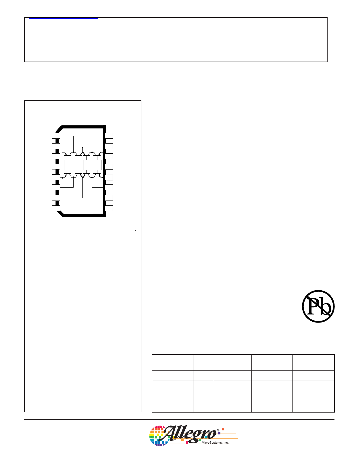
A3966SLB (SOIC)
OUT
PHASE
ENABLE
GROUND
SENSE
OUT
LOAD
SUPPLY
REFERENCE
1
1A
V
2
1
3
1
4
5
1
6
1B
710
V
89
REF
BB
LOGICLOGIC
V
BB
16
OUT
2A
PHASE
15
14
13
12
11
V
CC
RC
ENABLE
GROUND
SENSE
OUT
2B
LOGIC
SUPPLY
RC
Dwg. PP-066-1
2
2
2
ABSOLUTE MAXIMUM RATINGS
Load Supply Voltage, VBB...................... 30 V
Output Current, I
(continuous) .............................. ±650 mA
Logic Supply Voltage, V
Input Voltage, V
Sense Voltage, V
Package Power Dissipation (T
A3966SA ..................................... 2.08 W*
A3966SLB ................................... 1.87 W*
Operating Temperature Range,
T
..................................... -20°C to +85°C
A
Junction Temperature,
T
.................................................. +150°C
J
Storage Temperature Range,
T
................................... -55°C to +150°C
S
Output current rating may be limited by duty cycle,
ambient temperature, and heat sinking. Under any set
of conditions, do not exceed the specified current rating
or a junction temperature of 150°C.
* Per SEMI G42-88 Specification, Thermal Test Board
Standardization for Measuring Junction-to-Ambient
Thermal Resistance of Semiconductor Packages.
(peak) ........... ±750 mA
OUT
.................... 7.0 V
CC
........ -0.3 V to VCC + 0.3 V
in
................................ 1.0 V
S
= 25°C), P
A
D
29319.25C
3966
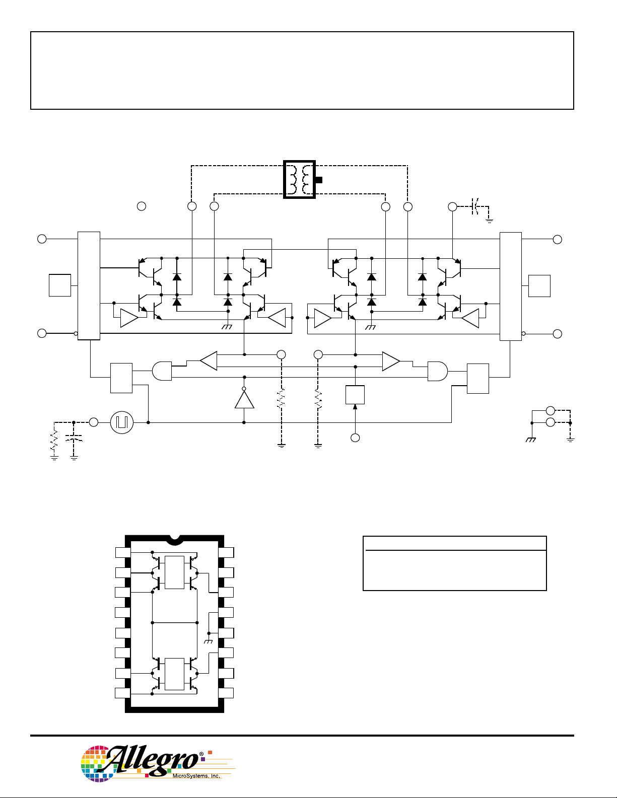
DUAL FULL-BRIDGE PWM
MOTOR DRIVER
The A3966SA and A3966SLB are designed to drive both windings of a twophase bipolar stepper motor. Each device includes two H-bridges capable of
continuous output currents of ±650 mA and operating voltages to 30 V. Motor
winding current can be controlled by the internal fixed-frequency, pulse-width
modulated (PWM), current-control circuitry. The peak load current limit is set
by the user’s selection of a reference voltage and current-sensing resistors.
Except for package style and pinout, the two devices are identical.
The fixed-frequency pulse duration is set by a user-selected external RC timing
network. The capacitor in the RC timing network also determines a userselectable blanking window that prevents false triggering of the PWM currentcontrol circuitry during switching transitions.
To reduce on-chip power dissipation, the H-bridge power outputs have been
optimized for low saturation voltages. The sink drivers feature the Allegro
patented Satlington® output structure. The Satlington outputs combine the low
voltage drop of a saturated transistor and the high peak current capability of a
Darlington.
For each bridge, a PHASE input controls load-current polarity by selecting the
appropriate source and sink driver pair. For each bridge, an ENABLE input, when
held high, disables the output drivers. Special power-up sequencing is not
required. Internal circuit protection includes thermal shutdown with hysteresis,
ground-clamp and flyback diodes, and crossover-current protection.
The A3966SA is supplied in a 16-pin dual in-line plastic package. The
A3966SLB is supplied in a 16-lead plastic SOIC with copper heat sink tabs. The
power tab is at ground potential and needs no electrical isolation. The A3966SLB
is also available in a lead (Pb) free version, with 100% matte tin leadframe plating.
FEATURES
■ ±650 mA Continuous Output Current
■ 30 V Output Voltage Rating
■ Internal Fixed-Frequency PWM Current Control
■ Satlington Sink Drivers
■ User-Selectable Blanking Window
■ Internal Ground-Clamp & Flyback Diodes
■ Internal Thermal-Shutdown Circuitry
■ Crossover-Current Protection and UVLO Protection
Always order by complete part number:
Part Number Pb-free Packing Package R
A3966SA – Bulk 16-pin DIP 60 38 —
A3966SLB – Bulk
A3966SLB-T Yes Bulk 16-lead SOIC 67 — 6
A3966SLBTR – Tape and Reel with internally
A3966SLBTR-T Yes Tape and Reel fused leads
R
θθ
θJA
θθ
(°C/W)
θθ
θJC
θθ
R
θθ
θJT
θθ
Data Sheet
®
3966
DUAL FULL-BRIDGE
PWM MOTOR DRIVER
LOGIC
SUPPLY
V
CC
PHASE
1
1
FUNCTIONAL BLOCK DIAGRAM
1A
1B
OUT
OUT
V
BB
2A
OUT
2B
OUT
LOAD
SUPPLY
+
PHASE
2
2
ENABLE
R
T
UVLO
& TSD
1
CONTROL LOGIC
1
SOURCE
ENABLE
RC
C
T
SENSE
OUT
LOAD
SUPPLY
REFERENCE
RC
LOGIC
SUPPLY
OUT
SENSE
PWM LATCH
Q
OSC
BLANKING
1
R
S
A3966SA (DIP)
1
1
2
1B
3
V
4
REF
RC
5
V
6
CC
7
2B
8
2
GATE
CURRENT-SENSE
1
LOGIC
V
BB
LOGIC
COMPARATOR
+
–
16
15
14
13
12
11
10
9
1
ENABLE
PHASE
OUT
GROUND
GROUND
OUT
PHASE
ENABLE
UVLO
& TSD
CONTROL LOGIC
ENABLE
2
÷4
REFERENCE
CURRENT-SENSE
COMPARATOR
+
–
2
BLANKING
GATE
2
PWM LATCH
R
S
2
2
SOURCE
ENABLE
Q
GROUND
Dwg. FP-036-6
SENSE
R
1S
SENSE
1
2
R
2S
TRUTH TABLE
PHASE ENABLE OUT
1
1
1A
XH OffOff
HL H L
LL L H
X = Irrelevant
2A
2
2
OUT
A
B
Dwg. PP-066-2
2
115 Northeast Cutoff, Box 15036
Worcester, Massachusetts 01615-0036 (508) 853-5000
Copyright © 1998, 2003 Allegro MicroSystems, Inc.

3966
DUAL FULL-BRIDGE
PWM MOTOR DRIVER
ELECTRICAL CHARACTERISTICS at T
V
= 0 V, 56 kΩ & 680 pF RC to Ground (unless noted otherwise)
S
= +25°C, V
A
= 30 V, VCC = 4.75 V to 5.5 V, V
BB
REF
= 2 V,
Limits
Characteristic Symbol Test Conditions Min. Typ. Max. Units
Output Drivers
Load Supply Voltage Range V
Output Leakage Current I
Output Saturation Voltage V
CE(SAT)
Clamp Diode Forward Voltage V
Motor Supply Current I
(No Load)
BB(ON)
I
BB(OFF)
BB
CEX
F
Operating, I
V
= 30 V — <1.0 50 µA
OUT
V
= 0 V — <-1.0 -50 µA
OUT
Source Driver, I
Source Driver, I
Sink Driver, I
Sink Driver, I
= ±650 mA, L = 3 mH V
OUT
= -400 mA — 1.7 2.0 V
OUT
= -650 mA — 1.8 2.1 V
OUT
= +400 mA, VS = 0.5 V — 0.3 0.5 V
OUT
= +650 mA, VS = 0.5 V — 0.7 1.3 V
OUT
CC
—30 V
IF = 400 mA — 1.1 1.4 V
IF = 650 mA — 1.4 1.6 V
V
V
ENABLE1
ENABLE1
= V
= V
= 0.8 V — 3.0 5.0 mA
ENABLE2
= 2.4 V — <1.0 200 µA
ENABLE2
Control Logic
Logic Supply Voltage Range V
Logic Input Voltage V
V
Logic Input Current I
I
Reference Input Volt. Range V
Reference Input Current I
Reference Divider Ratio V
REF/VTRIP
Current-Sense Comparator V
CC
IN(1)
IN(0)
IN(1)
IN(0)
REF
REF
IO
Operating 4.75 — 5.50 V
V
IN
V
IN
Operating 0.1 – 2.0 V
V
REF
Input Offset Voltage
Current-Sense Comparator V
S
Operating -0.3 — 1.0 V
Input Voltage Range
Sense-Current Offset I
SO
IS – I
NOTES: 1. Typical Data is for design information only.
2. Negative current is defined as coming out of (sourcing) the specified device terminal.
2.4 — — V
— — 0.8 V
= 2.4 V — <1.0 20 µA
= 0.8 V — <-20 -200 µA
-2.5 0 1.0 µA
3.8 4.0 4.2 —
= 0 V -6.0 0 6.0 mV
, 50 mA ≤ I
OUT
≤ 650 mA 12 18 24 mA
OUT
www.allegromicro.com
3

3966
DUAL FULL-BRIDGE
PWM MOTOR DRIVER
ELECTRICAL CHARACTERISTICS at T
V
= 0 V, 56 kΩ & 680 pF RC to Ground (unless noted otherwise) (cont.)
S
= +25°C, V
A
= 30 V, VCC = 4.75 V to 5.5 V, V
BB
REF
= 2 V,
Limits
Characteristic Symbol Test Conditions Min. Typ. Max. Units
Control Logic (continued)
PWM RC Frequency f
PWM Propagation Delay Time t
Cross-Over Dead Time t
PWM
codt
Propagation Delay Times t
Thermal Shutdown Temp. T
Thermal Shutdown Hysteresis ∆T
UVLO Enable Threshold V
UVLO Hysteresis V
Logic Supply Current I
T(UVLO)+
T(UVLO)hys
CC(ON)
I
CC(OFF)
osc
pd
J
J
CT = 680 pF, R
= 56 kΩ 22.9 25.4 27.9 kHz
T
Comparator Trip to Source OFF — 1.0 1.4 µs
Cycle Reset to Source ON — 0.8 1.2 µs
1 kΩ Load to 25 V 0.2 1.8 3.0 µs
I
= ±650 mA, 50% to 90%:
OUT
ENABLE ON to Source ON — 100 — ns
ENABLE OFF to Source OFF — 500 — ns
ENABLE ON to Sink ON — 200 — ns
ENABLE OFF to Sink OFF — 200 — ns
PHASE Change to Sink ON — 2200 — ns
PHASE Change to Sink OFF — 200 — ns
PHASE Change to Source ON — 2200 — ns
PHASE Change to Source OFF — 200 — ns
— 165 — °C
—15—°C
Increasing V
CC
— 4.1 4.6 V
0.1 0.6 — V
V
ENABLE 1
V
ENABLE 1
= V
= V
ENABLE 2
ENABLE 2
= 0.8 V — — 50 mA
= 2.4 V — — 9.0 mA
NOTES: 1. Typical Data is for design information only.
2. Negative current is defined as coming out of (sourcing) the specified device terminal.
4
115 Northeast Cutoff, Box 15036
Worcester, Massachusetts 01615-0036 (508) 853-5000

FUNCTIONAL DESCRIPTION
3966
DUAL FULL-BRIDGE
PWM MOTOR DRIVER
Internal PWM Current Control. The A3966SA and
A3966SLB dual H-bridges are designed to drive both
windings of a bipolar stepper motor. Load current can be
controlled in each motor winding by an internal fixedfrequency PWM control circuit. The current-control
circuitry works as follows: when the outputs of the Hbridge are turned on, current increases in the motor winding. The load current is sensed by the current-control
comparator via an external sense resistor (R
). Load
S
current continues to increase until it reaches the predetermined value, set by the selection of external currentsensing resistors and reference input voltage (V
REF
)
according to the equation:
I
where I
= I
TRIP
is the sense-current error (typically 18 mA) due
SO
+ ISO = V
OUT
REF
/(4 RS)
to the base-drive current of the sink driver transistor.
At the trip point, the comparator resets the sourceenable latch, turning off the source driver of that H-bridge.
The source turn off of one H-bridge is independent of the
other H-bridge. Load inductance causes the current to
recirculate through the sink driver and ground-clamp
diode. The current decreases until the internal clock
oscillator sets the source-enable latches of both H-bridges,
turning on the source drivers of both bridges. Load current
increases again, and the cycle is repeated.
V
PHASE
The frequency of the internal clock oscillator is set by
the external timing components R
. The frequency can
TCT
be approximately calculated as:
f
where t
osc
is defined below.
blank
= 1/(RT CT + t
blank
)
The range of recommended values for RT and CT are
20 kΩ to 100 kΩ and 470 pF to 1000 pF respectively.
Nominal values of 56 kΩ and 680 pF result in a clock
frequency of 25 kHz.
Current-Sense Comparator Blanking. When the
source driver is turned on, a current spike occurs due to
the reverse-recovery currents of the clamp diodes and
switching transients related to distributed capacitance in
the load. To prevent this current spike from erroneously
resetting the source enable latch, the current-control
comparator output is blanked for a short period of time
when the source driver is turned on. The blanking time is
set by the timing component C
according to the equa-
T
tion:
t
= 1900 CT (µs).
blank
A nominal C
value of 680 pF will give a blanking
T
time of 1.3 µs.
The current-control comparator is also blanked when
the H-bridge outputs are switched by the PHASE or
ENABLE inputs. This internally generated blank time is
approximately 1 µs.
V
BB
BRIDGE
+
I
0
OUT
–
www.allegromicro.com
ON
OSCILLATOR
BRIDGE
INTERNAL
ON
BRIDGE ON
ALL
OFF
SOURCE
I
TRIP
OFF
t
d
R C
T T
t
blank
Dwg. WM-003-2
R
S
SOURCE OFF
ALL OFF
Dwg. EP-006-16
5

3966
DUAL FULL-BRIDGE
PWM MOTOR DRIVER
FUNCTIONAL DESCRIPTION (continued)
Load Current Regulation. Due to internal logic and
switching delays (t
slightly higher than the I
), the actual load current peak will be
d
value. These delays, plus the
TRIP
blanking time, limit the minimum value the current control
circuitry can regulate. To produce zero current in a
winding, the ENABLE terminal should be held high,
turning off all output drivers for that H-bridge.
Logic Inputs. A logic high on the PHASE input results
in current flowing from OUT
to OUTB of that H-bridge.
A
A logic low on the PHASE input results in current flowing
from OUTB to OUTA. An internally generated dead time
(t
) of approximately 1 µs prevents cross-over current
codt
spikes that can occur when switching the PHASE input.
A logic high on the ENABLE input turns off all four
output drivers of that H-bridge. This results in a fast
current decay through the internal ground clamp and
flyback diodes. A logic low on the ENABLE input turns
on the selected source and sink driver of that H-bridge.
The ENABLE inputs can be pulse-width modulated for
applications that require a fast current-decay PWM. If
external current-sensing circuitry is used, the internal
current-control logic can be disabled by connecting the
RTCT terminal to ground.
The REFERENCE input voltage is typically set with a
resistor divider from V
. This reference voltage is
CC
internally divided down by 4 to set up the current-comparator trip-voltage threshold. The reference input voltage
range is 0 to 2 V.
Output Drivers. To minimize on-chip power dissipation,
the sink drivers incorporate a Satlington structure. The
Satlington output combines the low V
features of a
CE(sat)
saturated transistor and the high peak-current capability of
a Darlington (connected) transistor. A graph showing
typical output saturation voltages as a function of output
current is on the next page.
Miscellaneous Information. Thermal protection
circuitry turns off all output drivers should the junction
temperature reach +165 °C (typical). This is intended
only to protect the device from failures due to excessive
junction temperatures and should not imply that output
short circuits are permitted. Normal operation is resumed
when the junction temperature has decreased about 15°C.
The A3966 current control employs a fixed-frequency, variable duty cycle PWM technique. As a result,
the current-control regulation may become unstable if the
duty cycle exceeds 50%.
To minimize current-sensing inaccuracies caused by
ground trace I
drops, each current-sensing resistor
R
should have a separate return to the ground terminal of
the device. For low-value sense resistors, the I x R drops
in the printed-wiring board can be significant and should
be taken into account. The use of sockets should be
avoided as their contact resistance can cause variations in
the effective value of RS.
The LOAD SUPPLY terminal, VBB, should be
decoupled with an electrolytic capacitor (47 µF recommended) placed as close to the device as physically
practical. To minimize the effect of system ground I x R
drops on the logic and reference input signals, the system
ground should have a low-resistance return to the load
supply voltage.
The frequency of the clock oscillator will determine
the amount of ripple current. A lower frequency will
result in higher current ripple, but reduced heating in the
motor and driver IC due to a corresponding decrease in
hysteretic core losses and switching losses respectively.
A higher frequency will reduce ripple current, but will
increase switching losses and EMI.
6
115 Northeast Cutoff, Box 15036
Worcester, Massachusetts 01615-0036 (508) 853-5000

Typical output saturation
voltages showing Satlington
sink-driver operation.
3966
DUAL FULL-BRIDGE
PWM MOTOR DRIVER
2.5
TA = +25°C
2.0
SOURCE DRIVER
1.5
1.0
56 kW
PH2
TYPICAL APPLICATION
(A3966SLB)
0.5 W
680 pF
+3.3 V
28272625242322
1
2
3
4
LOGIC
5
6
7
8
9
1011121314
+24 V
LOGIC
V
BB
0.5
SINK DRIVER
OUTPUT SATURATION VOLTAGE IN VOLTS
+3.3 V
47 µF
20 kW
10 kW
0
200
OUTPUT CURRENT IN MILLIAMPERES
The products described here are manufactured under one or more
500
600
007004300
Dwg. GP-064-1A
U.S. patents or U.S. patents pending. Satlington® is a registered
21
20
0.5 W
19
18
17
16
15
EN1EN2
PH1
trademark of Allegro MicroSystems, Inc. (Allegro), and Satlington
devices are manufactured under U. S. Patent No. 5,684,427.
Allegro MicroSystems, Inc. reserves the right to make, from time to
time, such departures from the detail specifications as may be
required to permit improvements in the performance, reliability, or
manufacturability of its products. Before placing an order, the user is
cautioned to verify that the information being relied upon is current.
Allegro products are not authorized for use as critical components
in life-support devices or systems without express written approval.
The information included herein is believed to be accurate and
reliable. However, Allegro MicroSystems, Inc. assumes no responsibility for its use; nor for any infringement of patents or other rights of
third parties which may result from its use.
www.allegromicro.com
7

3966
DUAL FULL-BRIDGE
PWM MOTOR DRIVER
16
0.280
0.240
A3966SA
Dimensions in Inches
(controlling dimensions)
9
0.014
0.008
0.430
MAX
0.300
BSC
0.210
MAX
7.11
6.10
0.015
MIN
1
0.070
0.045
16
1
1.77
1.15
0.022
0.014
0.100
0.775
0.735
BSC
Dimensions in Millimeters
(for reference only)
2.54
19.68
18.67
BSC
8
0.005
MIN
0.150
0.115
Dwg. MA-001-16A in
0.355
9
8
0.13
MIN
0.204
10.92
MAX
7.62
BSC
5.33
MAX
0.39
MIN
0.558
0.356
3.81
2.93
NOTES: 1. Exact body and lead configuration at vendor’s option within limits shown.
2. Lead spacing tolerance is non-cumulative.
3. Lead thickness is measured at seating plane or below.
4. Supplied in standard sticks/tubes of 25 devices.
8
115 Northeast Cutoff, Box 15036
Worcester, Massachusetts 01615-0036 (508) 853-5000
Dwg. MA-001-16A mm

A3966SLB
Dimensions in Inches
(for reference only)
16 9
3966
DUAL FULL-BRIDGE
PWM MOTOR DRIVER
0.0125
0.0091
0.2992
0.2914
0.020
0.013
0.0926
0.1043
7.60
7.40
1 2
0.0040
MIN.
3
0.4133
0.3977
Dimensions in Millimeters
(controlling dimensions)
0.419
0.394
0.050
0.016
0.050
BSC
916
0° TO 8°
Dwg. MA-008-16A in
0.32
0.23
10.65
10.00
0.51
0.33
2.65
2.35
1 2
0.10
3
10.50
10.10
MIN.
1.27
BSC
NOTES: 1. Exact body and lead configuration at vendor’s option within limits shown.
2. Lead spacing tolerance is non-cumulative.
3. Webbed lead frame. Leads 4 and 13 are internally one piece.
4. Supplied in standard sticks/tubes of 47 devices or add “TR” to part number for tape and reel.
www.allegromicro.com
1.27
0.40
0° TO 8°
Dwg. MA-008-16A mm
9

 Loading...