

查询A3959供应商查询A3959供应商
3959
DMOS FULL-BRIDGE PWM
29319.37E
MOTOR DRIVER
Data Sheet
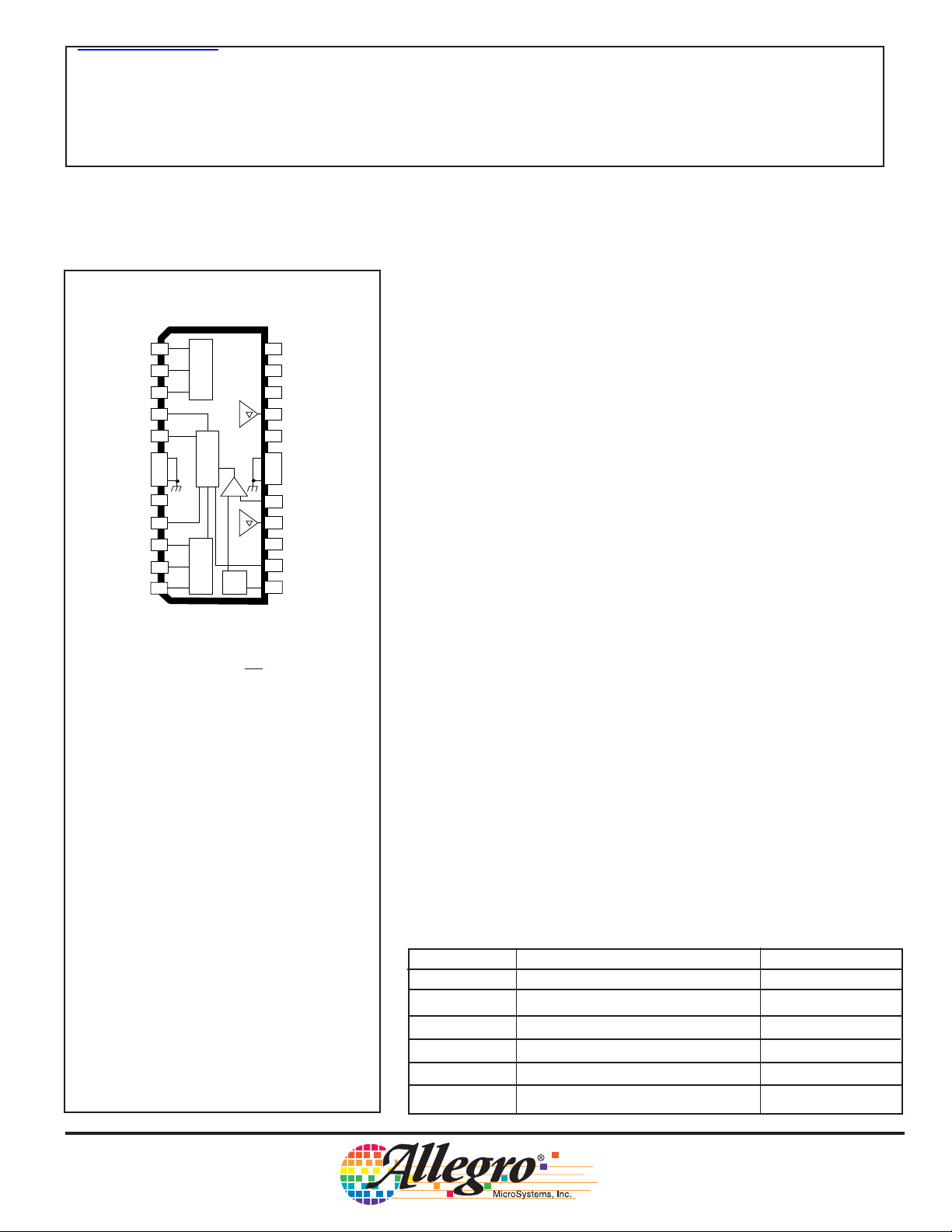
A3959SLB (SOIC)
Designed for pulse-width modulated (PWM) current control of dc
motors, the A3959SB, A3959SLB, and A3959SLP are capable of
output currents to ±3 A and operating voltages to 50 V. Internal fixed
V
24
REG
23
SLEEP
NO
NC
22
CONNECTION
21
B
OUT
V
20
LOAD SUPPLY
BB
19
GROUND
18
GROUND
SENSE
17
A
OUT
16
NO
NC
15
CONNECTION
EXT MODE
14
REF
13
Dwg. PP-069-4
CP
PHASE
ROSC
GROUND
GROUND
LOGIC SUPPLY
ENABLE
PFD
BLANK
PFD
CP
1
2
2
CP
1
3
4
5
6
7
8
9
9
2
10
11
1
12
θ
V
DD
CHARGE PUMP
LOGIC
÷
10
PWM TIMER
Note that the A3959SLB(SOIC), A3959SB (DIP),
and A3959SLP (TSSOP) do
not share a common
terminal assignment.
off-time PWM current-control timing circuitry can be adjusted via
control inputs to operate in slow, fast, and mixed current-decay modes.
PHASE and ENABLE input terminals are provided for use in
controlling the speed and direction of a dc motor with externally
applied PWM-control signals. Internal synchronous rectification
control circuitry is provided to reduce power dissipation during PWM
operation.
Internal circuit protection includes thermal shutdown with
hysteresis, undervoltage monitoring of supply and charge pump, and
crossover-current protection. Special power-up sequencing is not
required.
The A3959SB/SLB/SLP is a choice of three power packages, a
24-pin plastic DIP with a copper batwing tab (package suffix ‘B’), a
24-lead plastic SOIC with a copper batwing tab (package suffix ‘LB’),
and a thin (<1.2 mm) 28-lead plastic TSSOP with an exposed thermal
pad (suffix ‘LP’). In all cases, the power tab is at ground potential and
needs no electrical isolation.
free version (100% matte tin leadframe).
ABSOLUTE MAXIMUM RATINGS
Load Supply Voltage, VBB......................... 50 V
Output Current, I
(Repetitive) ........... ±3.0 A
OUT
(Peak, <3 µs) ................................... ±6.0 A
Logic Supply Voltage, VDD....................... 7.0 V
Logic Input Voltage Range, V
IN
(Continuous) ............ -0.3 V to VDD + 0.3 V
<30 ns) ............... -1.0 V to VDD + 1.0 V
(t
w
Sense Voltage, VS (Continuous) .............. 0.5 V
(tw <3 µs) ........................................... 2.5 V
Reference Voltage, V
Package Power Dissipation (TA = 25°C), P
............................ V
REF
DD
D
A3959SB ........................................ 3.3 W*
A3959SLB ...................................... 2.5 W*
A3959SLP ...................................... 3.1 W*
Operating Temp. Range, T
.... -20°C to +85°C
A
Junction Temperature, TJ..................... +150°C
Storage Temp. Range, TS..... -55°C to +150°C
Output current rating may be limited by duty cycle,
ambient temperature, and heat sinking. Under any
set of conditions, do not exceed the specified
current rating or a junction temperature of 150°C.
* Double-sided board, one square inch copper each side. See also, Layout, page 7.
FEATURES
■ ±3 A, 50 V Output Rating
■ Low
■ Mixed, Fast, and Slow Current-Decay Modes
■ Synchronous Rectification for Low Power Dissipation
■ Internal UVLO and Thermal-Shutdown Circuitry
■ Crossover-Current Protection
■ Internal Oscillator for Digital PWM Timing
Always order by complete part number:
Part Number Package R
A3959SB-T 24-pin batwing DIP; Lead-free 38°C/W 6°C/W
A3959SLB 24-lead batwing SOIC 50°C/W 6°C/W
A3959SLB-T 24-lead batwing SOIC; Lead-free 50°C/W 6°C/W
A3959SLP 28-lead thin shrink SOIC 40°C/W —
A3959SLP-T 28-lead thin shrink SOIC; Lead-free 40°C/W —
r
Outputs (270 mΩ, Typical)
DS(on)
A3959SB 24-pin batwing DIP 38°C/W 6°C/W
Each package is available in a lead-
* R
θθ
θJA
θθ
θθ
θJT
θθ
3959
DMOS FULL-BRIDGE
PWM MOTOR DRIVER
V
DD
LOGIC
SUPPLY
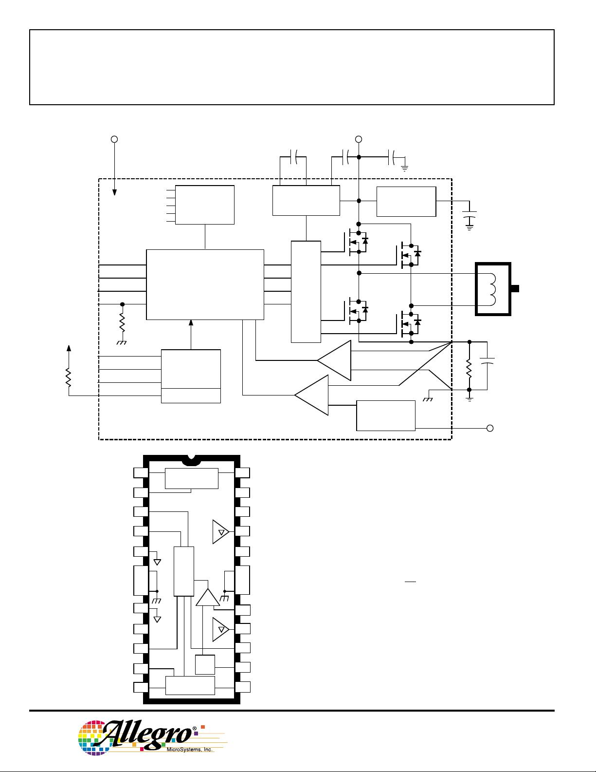
FUNCTIONAL BLOCK DIAGRAM
VBB
CP1
CP2
CP
LOAD
SUPPLY
+
SLEEP
EXT MODE
PHASE
ENABLE
TO VDD
BLANK
PFD1
PFD2
ROSC
CHARGE PUMP
CP
PHASE
2
1
BANDGAP
V
C
REG
TSD
1
2
θ
3
VOLTAGE &
DD
FAULT DETECT
CONTROL LOGIC
PWM
TIMER
OSC
CHARGE PUMP
UNDER-
CHARGE
PUMP
BANDGAP
REGULATOR
VREG
OUTA
GATE DRIVE
OUTB
SENSE
ZERO
CURRENT
DETECT
CURRENT
SENSE
CPCP
24
REG
V
23
SLEEP
22
REFERENCE
BUFFER &
÷10
REF
CS
RS
V
Dwg. FP-048-2A
REF
ROSC
GROUND
GROUND
GROUND
GROUND
LOGIC
SUPPLY
ENABLE
BLANK
2
PFD
4
5
6
7
8
9
V
9
10
2
11
12
LOGIC
DD
PWM TIMER
V
BB
÷
10
21
20
19
18
17
16
15
14
13
OUT
B
LOAD
SUPPLY
GROUND
GROUND
SENSE
OUT
A
EXT MODE
REF
PFD
1
Dwg. PP-069-5A
A3959SB (DIP)
Note that the A3959SLB (SOIC), A3959SB (DIP),
and A3959SLP (TSSOP) do
terminal assignment.
not share a common
115 Northeast Cutoff, Box 15036
Worcester, Massachusetts 01615-0036 (508) 853-5000
Copyright © 2001, 2003 Allegro MicroSystems, Inc.
3959
DMOS FULL-BRIDGE
PWM MOTOR DRIVER
ELECTRICAL CHARACTERISTICS at T
f
< 50 kHz (unless noted otherwise)
PWM
= +25°C, V
A
= 50 V, VDD = 5.0 V, V
BB
SENSE
= 0.5 V,
Limits
Characteristics Symbol Test Conditions Min. Typ. Max. Units
Output Drivers
Load Supply Voltage Range V
BB
Operating 9.5 – 50 V
During sleep mode 0 – 50 V
Output Leakage Current I
Output On Resistance r
DSS
DS(on)
V
= V
OUT
V
OUT
Source driver, I
Sink driver, I
BB
= 0 V – <-1.0 -20 µA
= -3 A – 270 300 mΩ
OUT
= 3 A – 270 300 mΩ
OUT
– <1.0 20 µA
Crossover Delay 300 600 1000 ns
Body Diode Forward Voltage V
Source diode, IF = -3 A – – 1.6 V
F
Sink diode, IF = 3 A – – 1.6 V
Load Supply Current I
BB
f
< 50 kHz – 4.0 7.0 mA
PWM
Charge pump on, outputs disabled – 2.0 5.0 mA
Control Logic
Logic Supply Voltage Range V
Logic Input Voltage V
V
Logic Input Current I
(all inputs except ENABLE)
I
ENABLE Input Current I
I
Internal OSC frequency f
Reference Input Volt. Range V
Reference Input Current I
Comparator Input Offset Volt. V
DD
IN(1)
IN(0)
IN(1)
IN(0)
IN(1)
IN(0)
OSC
REF
REF
IO
Sleep Mode – – 20 µA
Operating 4.5 5.0 5.5 V
2.0 – – V
– – 0.8 V
V
= 2.0 V – <1.0 20 µA
IN
V
= 0.8 V – <-2.0 -20 µA
IN
V
= 2.0 V – 40 100 µA
IN
V
= 0.8 V – 16 40 µA
IN
R
shorted to GROUND 3.25 4.25 5.25 MHz
OSC
R
= 51 kΩ 3.65 4.25 4.85 MHz
OSC
Operating 0.0 – V
V
= V
V
REF
REF
DD
= 0 V – ±5.0 – mV
––±1.0 µA
Continued next page …
DD
V
www.allegromicro.com
3

3959
DMOS FULL-BRIDGE
PWM MOTOR DRIVER
ELECTRICAL CHARACTERISTICS at T
f
< 50 kHz (unless noted otherwise), continued.
PWM
= +25°C, V
A
= 50 V, VDD = 5.0 V, V
BB
SENSE
= 0.5 V,
Limits
Characteristics Symbol Test Conditions Min. Typ. Max. Units
Control Logic
Reference Divider Ratio – – 10 – –
Gm Error E
Gm
(Note 3) V
Propagation Delay Times t
pd
V
= V
REF
REF
0.5 Ein to 0.9 E
DD
= 0.5 V – – ±14 %
:
out
––±4.0 %
PWM change to source on 600 750 1200 ns
PWM change to source off 50 150 350 ns
PWM change to sink on 600 750 1200 ns
PWM change to sink off 50 100 150 ns
Thermal Shutdown Temp. T
Thermal Shutdown Hysteresis ∆T
J
J
UVLO Enable Threshold UVLO Increasing V
DD
– 165 – °C
–15– °C
3.90 4.2 4.45 V
UVLO Hysteresis ∆UVLO 0.05 0.10 – V
Logic Supply Current I
DD
f
< 50 kHz – 6.0 10 mA
PWM
Sleep Mode – – 2.0 mA
NOTES: 1. Typical Data is for design information only.
2. Negative current is defined as coming out of (sourcing) the specified device terminal.
3. Gm error = ([V
4
/10] – V
REF
SENSE
)/(V
REF
115 Northeast Cutoff, Box 15036
Worcester, Massachusetts 01615-0036 (508) 853-5000
/10) where V
SENSE
= I
TRIP•RS
.

FUNCTIONAL DESCRIPTION
3959
DMOS FULL-BRIDGE
PWM MOTOR DRIVER
V
. This internally generated voltage is used to operate
REG
the sink-side DMOS outputs. The V
be decoupled with a 0.22 µF capacitor to ground. V
terminal should
REG
REG
is
internally monitored and in the case of a fault condition,
the outputs of the device are disabled.
Charge Pump. The charge pump is used to generate a
gate-supply voltage greater than V
to drive the source-
BB
side DMOS gates. A 0.22 µF ceramic capacitor should be
connected between CP1 and CP2 for pumping purposes.
A 0.22 µF ceramic capacitor should be connected between
CP and V
to act as a reservoir to operate the high-side
BB
DMOS devices. The CP voltage is internally monitored
and, in the case of a fault condition, the source outputs of
the device are disabled.
PHASE Logic. The PHASE input terminal determines if
the device is operating in the “forward” or “reverse” state.
PHASE OUT
A
OUT
B
0 Low High
1 High Low
ENABLE Logic. The ENABLE input terminal allows
external PWM. ENABLE high turns on the selected sinksource pair. ENABLE low switches off the source driver
or the source and sink driver, depending on EXT MODE,
and the load current decays. If ENABLE is kept high, the
current will rise until it reaches the level set by the internal
current-control circuit.
ENABLE Outputs
0 Chopped
1On
EXT MODE Logic. When using external PWM current
control, the EXT MODE input determines the current path
during the chopped cycle. With EXT MODE low, fast
decay mode, the opposite pair of selected outputs will be
enabled during the off cycle. With EXT MODE high,
slow decay mode, both sink drivers are on with ENABLE
low.
EXT MODE Decay
0 Fast
1 Slow
Current Regulation. Load current is regulated by an
internal fixed off-time PWM control circuit. When the
outputs of the DMOS H bridge are turned on, the current
increases in the motor winding until it reaches a trip value
determined by the external sense resistor (R
applied analog reference voltage (V
I
= V
TRIP
REF
/10R
REF
S
):
) and the
S
At the trip point, the sense comparator resets the sourceenable latch, turning off the source driver. The load
inductance then causes the current to recirculate for the
fixed off-time period. The current path during
recirculation is determined by the configuration of slow/
mixed/fast current-decay mode via PFD1 and PFD2.
Oscillator. The PWM timer is based on an internal
oscillator set by a resistor connected from the R
OSC
terminal to VDD. Typical value of 4 MHz is set with a
51 kΩ resistor. The allowable range of the resistor is from
20 kΩ to 100 kΩ.
f
If R
= 204 x 109/R
OSC
is not pulled up to VDD, it must be shorted to
OSC
OSC
.
ground.
www.allegromicro.com
Fixed Off Time. The A3959 is set for a fixed off time of
96 cycles of the internal oscillator, typically 24 µs with a
4 MHz oscillator.
5

3959
DMOS FULL-BRIDGE
PWM MOTOR DRIVER
FUNCTIONAL DESCRIPTION (continued)
Internal Current-Control Mode. Inputs PFD1 and
PFD2 determine the current-decay method after an
overcurrent event is detected at the SENSE input. In
slow-decay mode, both sink drivers are turned on for the
fixed off-time period. Mixed-decay mode starts out in
fast-decay mode for a portion (15% or 48%) of the fixed
off time, and then is followed by slow decay for the
remainder of the period.
PFD2 PFD1 % t
off
Decay
0 0 0 Slow
0 1 15 Mixed
1 0 48 Mixed
1 1 100 Fast
PWM Blank Timer. When a source driver turns on, a
current spike occurs due to the reverse-recovery currents
of the clamp diodes and/or switching transients related to
distributed capacitance in the load. To prevent this current
spike from erroneously resetting the source-enable latch,
the sense comparator is blanked. The blank timer runs
after the off-time counter to provide the blanking function.
The blank timer is reset when ENABLE is chopped or
PHASE is changed. For external PWM control, a PHASE
change or ENABLE on will trigger the blanking function.
The duration is determined by the BLANK input and the
oscilator.
BLANK t
0 6/f
1 12/f
blank
osc
osc
Synchronous Rectification. When a PWM off cycle
is triggered, either by an ENABLE chop command or
internal fixed off-time cycle, load current will recirculate
according to the decay mode selected by the control logic.
The A3959 synchronous rectification feature will turn on
the appropriate pair of DMOS outputs during the current
decay and effectively short out the body diodes with the
low r
driver. This will reduce power dissipation
DS(on)
significantly and can eliminate the need for external
Schottky diodes.
Synchronous rectification will prevent reversal of load
current by turning off all outputs when a zero-current level
is detected.
Shutdown. In the event of a fault (excessive junction
temperature, or low voltage on CP or V
) the outputs of
REG
the device are disabled until the fault condition is
removed. At power up, and in the event of low V
DD
, the
UVLO circuit disables the drivers.
Braking. The braking function is implemented by
driving the device in slow-decay mode via EXTMODE
and applying an enable chop command. Because it is
possible to drive current in either direction through the
DMOS drivers, this configuration effectively shorts out
the motor-generated BEMF as long as the ENABLE chop
mode is asserted. It is important to note that the internal
PWM current-control circuit will not limit the current
when braking, because the current does not flow through
the sense resistor. The maximum brake current can be
approximated by V
BEMF/RL
. Care should be taken to
ensure that the maximum ratings of the device are not
exceeded in worst-case braking situations of high speed
and high inertial loads.
SLEEP Logic. The SLEEP input terminal is used to
minimize power consumption when when not in use. This
disables much of the internal circuitry including the
regulator and charge pump. Logic low will put the device
into sleep mode, logic high will allow normal operation.
6
115 Northeast Cutoff, Box 15036
Worcester, Massachusetts 01615-0036 (508) 853-5000

DMOS FULL-BRIDGE
PWM MOTOR DRIVER
FUNCTIONAL DESCRIPTION (continued)
3959
Current Sensing. To minimize inaccuracies in sensing
the I
current level, which may be caused by ground
TRIP
trace IR drops, the sense resistor should have an
independent ground return to the ground terminal of the
device. For low-value sense resistors the IR drops in the
PCB sense resistor’s traces can be significant and should
be taken into account. The use of sockets should be
avoided as they can introduce variation in R
due to their
S
contact resistance.
The maximum value of R
where I
TRIP
≤ 3.0 A.
is given as RS ≤ 0.5/I
S
TRIP
Thermal Protection. Circuitry turns off all drivers
when the junction temperature reaches 165°C typically. It
is intended only to protect the device from failures due to
excessive junction temperatures and should not imply that
output short circuits are permitted. Thermal shutdown has
a hysteresis of approximately 15°C.
5
SUFFIX 'B', R
SUFFIX 'LP', R
4
SUFFIX 'LB', R
MULTI-LAYER HIGH-K BOARD
θJA
= 26°C/W
θJA
θJA
= 28°C/W
= 35°C/W
Layout. A star ground system located close to the driver
is recommended. The printed wiring board should use a
heavy ground plane. For optimum electrical and thermal
performance*, the driver should be soldered directly onto
the board. The ground side of R
should have an indi-
S
vidual path to the ground terminals of the device. This
path should be as short as is possible physically and
should not have any other components connected to it. It
is recommended that a 0.1 µF capacitor be placed between
SENSE and ground as close to the device as possible; the
load supply terminal, V
, should be decoupled with an
BB
electrolytic capacitor (> 47 µF is recommended) placed as
close to the device as is possible. On the 28-lead TSSOP
package, the copper ground plane located under the
exposed thermal pad is typically used as a star ground.
* The thermal resistance, R
, and absolute maximum
θJA
allowable package power dissipation specified on page 1
is measured on a typical two-sided PCB with one square
inch copper ground area on each side. With minimal
copper on a single-sided PCB (worst-case), the ‘B’
package R
is 40°C/W, ‘LB’ is 77°C/W, and ‘LP’ is
θJA
80°C/W. See also, Application Note 29501.5, Improving
Batwing Power Dissipation.
3
2
1
SUFFIX 'B', R
SUFFIX 'LP', R
SUFFIX 'LB', R
DOUBLE-SIDED BOARD,
1 SQ. IN. COPPER EA. SIDE
0
25
ALLOWABLE PACKAGE POWER DISSIPATION IN WATTS
www.allegromicro.com
θJA
= 38°C/W
θJA
= 40°C/W
θJA
= 50°C/W
50 75 100 125 150
TEMPERATURE IN °°°°C
Dwg. GP-049-6
For specification purposes, the multi-layer high-K board
performance graphed here is per JEDEC Standard
JESD51.
The products described here are manufactured under one or more
U.S. patents or U.S. patents pending.
Allegro MicroSystems, Inc. reserves the right to make, from time to
time, such departures from the detail specifications as may be
required to permit improvements in the performance, reliability, or
manufacturability of its products. Before placing an order, the user is
cautioned to verify that the information being relied upon is current.
Allegro products are not authorized for use as critical components
in life-support devices or systems without express written approval.
The information included herein is believed to be accurate and
reliable. However, Allegro MicroSystems, Inc. assumes no responsibility for its use; nor for any infringement of patents or other rights of
third parties which may result from its use.
7

3959
DMOS FULL-BRIDGE
PWM MOTOR DRIVER
Terminal List
LB B LP
Terminal Name Terminal Description (SOIC) (DIP) (TSSOP)
CP Reservoir capacitor (typically 0.22 µF) 1 24 1
CP1 & CP2 The charge pump capacitor (typically 0.22 µF) 2 & 3 1 & 2 2 & 3
NC No (internal) connection — — 4
PHASE Logic input for direction control 4 3 5
ROSC Oscillator resistor 5 4 6
GROUND Grounds 6, 7 5, 6, 7, 8* 7, 8*
LOGIC SUPPLY V
ENABLE Logic input for enable control 9 10 10
NC No (internal) connection – – 11
PFD
2 Logic-level input for fast decay 10 11 12
BLANK Logic-level input for blanking control 11 12 13
PFD1 Logic-level input for fast decay 12 13 14
REF V
EXT MODE Logic input for PWM mode control 14 15 16
NO CONNECT No (Internal) connection 15 — 17
OUT
A
NC No (internal) connection – – 19, 20
SENSE Sense resistor 17 17 21
NC No (internal) connection – – 22
GROUND Grounds 18, 19 18, 19* —
LOAD SUPPLY V
OUT
B
NO CONNECT No (Internal) connection 22 — 25
SLEEP Logic-level Input for sleep operation 23 22 26
V
REG
GROUND Ground — — 28*
, the low voltage (typically 5 V) supply 8 9 9
DD
, the load current reference input voltage 13 14 15
REF
One of two DMOS bridge outputs to the motor 16 16 18
, the high-current, 9.5 V to 50 V, motor supply 20 20 23
BB
One of two DMOS bridge outputs to the motor 21 21 24
Regulator decoupling capacitor (typically 0.22 µF) 24 23 27
* For the A3959SB (DIP) only, there is an indeterminate resistance between the substrate grounds (pins 6, 7,
18, and 19) and the grounds at pins 5 and 8. Pins 5 and 8, and 6, 7, 18, or 19 must be connected together
externally. For the A3959SLP (TSSOP) the grounds at terminals 7, 8, and 28 should be connected together at
the exposed pad beneath the device.
8
115 Northeast Cutoff, Box 15036
Worcester, Massachusetts 01615-0036 (508) 853-5000

0.280
0.240
24
NOTE 1
A3959SB
Dimensions in Inches
(controlling dimensions)
13
3959
DMOS FULL-BRIDGE
PWM MOTOR DRIVER
0.014
0.008
0.430
MAX
0.300
BSC
0.210
MAX
7.11
6.10
0.015
MIN
16
0.070
0.045
0.022
0.014
24
1
1.77
1.15
7
NOTE 1
67
12
1.280
1.230
0.100
BSC
Dimensions in Millimeters
(for reference only)
13
12
32.51
31.24
2.54
BSC
0.005
0.150
0.115
0.13
MIN
MIN
0.355
0.204
Dwg. MA-001-25A in
10.92
MAX
7.62
BSC
5.33
MAX
0.39
MIN
0.558
0.356
NOTES: 1. Webbed lead frame. Leads 6, 7, 18, and 19 are internally one piece.
2. Exact body and lead configuration at vendor’s option within limits shown.
3. Lead spacing tolerance is non-cumulative.
4. Lead thickness is measured at seating plane or below.
5. Supplied in standard sticks/tubes of 15 devices.
www.allegromicro.com
3.81
2.93
Dwg. MA-001-25A mm
9

3959
DMOS FULL-BRIDGE
PWM MOTOR DRIVER
A3959SLB
0.2992
0.2914
0.020
0.013
0.0926
0.1043
24 13
1
2
3
0.6141
0.5985
0.0040
MIN.
0.050
BSC
NOTE 1
NOTE 3
0.419
0.394
0° TO 8°
0.0125
0.0091
0.050
0.016
Dwg. MA-008-25A in
Dimensions in Inches
(for reference only)
0.32
0.23
7.60
7.40
0.51
0.33
2.65
2.35
1242
0.10
MIN.
3
15.60
15.20
1.27
BSC
NOTE 1
NOTE 3
10.65
10.00
NOTES: 1. Exact body and lead configuration at vendor’s option within limits shown.
2. Lead spacing tolerance is non-cumulative.
3. Webbed lead frame. Leads 6, 7, 18, and 19 are internally one piece.
4. Supplied in standard sticks/tubes of 31 devices or add “TR” to part number for tape and reel.
10
115 Northeast Cutoff, Box 15036
Worcester, Massachusetts 01615-0036 (508) 853-5000
Dimensions in Millimeters
(controlling dimensions)
1.27
0.40
0° TO 8°
Dwg. MA-008-25A mm

3959
DMOS FULL-BRIDGE
PWM MOTOR DRIVER
A3959SLP
28-pin TSSOP
9.8
.386
9.6
.378
28
8”
0”
0.20
.008
0.09
.004
6.6
6.2
.260
.244
0.30
0.19
0.30
BSC
0.75
BSC
5
BSC
4.5
BSC
.200
0.65
BSC
0.65
BSC
A
.026
.026
.138
4.5
.177
4.3
.169
21
.012
.007
.012
6.6
.260
BSC
.030
Dimensions in millimeters
U.S. Customary dimensions (in.) in brackets, for reference only
A
Exposed thermal pad (bottom surface)
2.7
BSC
.106
0.75
0.45
3
BSC
.118
.030
.018
0.15
0.00
1.20
MAX
.006
.000
.047
1
.039
REF
0.25
.010
BSC
Seating Plane
Gauge Plane
www.allegromicro.com
11

3959
DMOS FULL-BRIDGE
PWM MOTOR DRIVER
MOTOR DRIVERS
Function Output Ratings* Part Number
INTEGRATED CIRCUITS FOR BRUSHLESS DC MOTORS
3-Phase Power MOSFET Controller — 28 V 3933
3-Phase Power MOSFET Controller — 40 V 3935
3-Phase Power MOSFET Controller — 50 V 3932 & 3938
3-Phase Back-EMF Controller/Driver ±900 mA 14 V 8904
3-Phase PWM Current-Controlled DMOS Driver ±3.0 A 50 V 3936
INTEGRATED BRIDGE DRIVERS FOR DC AND BIPOLAR STEPPER MOTORS
PWM Current-Controlled Dual Full Bridge ±500 mA 18 V 3965
Dual Full Bridge with Protection & Diagnostics ±500 mA 30 V 3976
PWM Current-Controlled Dual Full Bridge ±650 mA 30 V 3966
PWM Current-Controlled Dual Full Bridge ±650 mA 30 V 3968
Microstepping Translator/Dual Full Bridge ±750 mA 30 V 3967
PWM Current-Controlled Dual Full Bridge ±750 mA 45 V 2916
PWM Current-Controlled Dual Full Bridge ±750 mA 45 V 2919
PWM Current-Controlled Dual Full Bridge ±750 mA 45 V 6219
PWM Current-Controlled Dual Full Bridge ±800 mA 33 V 3964
PWM Current-Controlled Dual DMOS Full Bridge ±1.0 A 35 V 3973
PWM Current-Controlled Full Bridge ±1.3 A 50 V 3953
PWM Current-Controlled Dual Full Bridge ±1.5 A 45 V 2917
PWM Current-Controlled DMOS Full Bridge ±1.5 A 50 V 3948
PWM Current-Controlled Microstepping Full Bridge ±1.5 A 50 V 3955
PWM Current-Controlled Microstepping Full Bridge ±1.5 A 50 V 3957
PWM Current-Controlled Dual DMOS Full Bridge ±1.5 A 50 V 3972
PWM Current-Controlled Dual DMOS Full Bridge ±1.5 A 50 V 3974
PWM Current-Controlled Full Bridge ±2.0 A 50 V 3952
PWM Current-Controlled DMOS Full Bridge ±2.0 A 50 V 3958
Microstepping Translator/Dual DMOS Full Bridge ±2.5 A 35 V 3977
PWM Current-Controlled DMOS Full Bridge ±3.0 A 50 V 3959
UNIPOLAR STEPPER MOTOR & OTHER DRIVERS
Unipolar Stepper-Motor Translator/Driver 1.0 A 46 V 7050
Unipolar Stepper-Motor Translator/Driver 1.25 A 50 V 5804
Unipolar Stepper-Motor Quad Drivers 1.5 A 46 V 7024 & 7029
Unipolar Microstepper-Motor Quad Driver 1.5 A 46 V 7042
Unipolar Stepper-Motor Quad Driver 1.8 A 50 V 2540
Unipolar Stepper-Motor Translator/Driver 2.0 A 46 V 7051
Unipolar Stepper-Motor Quad Driver 3.0 A 46 V 7026
Unipolar Microstepper-Motor Quad Driver 3.0 A 46 V 7044
Unipolar Stepper-Motor Translator/Driver 3.0 A 46 V 7052
* Current is maximum specified test condition, voltage is maximum rating. See specification for sustaining voltage limits
or over-current protection voltage limits. Negative current is defined as coming out of (sourcing) the output.
† Complete part number includes additional characters to indicate operating temperature range and package style.
Also, see 3175, 3177, 3235, and 3275 Hall-effect sensors for use with brushless dc motors.
†
12
115 Northeast Cutoff, Box 15036
Worcester, Massachusetts 01615-0036 (508) 853-5000
 Loading...