

查询3955供应商
1
PFD
2
REF
3
RC
GROUND
GROUND
LOGIC
SUPPLY
PHASE
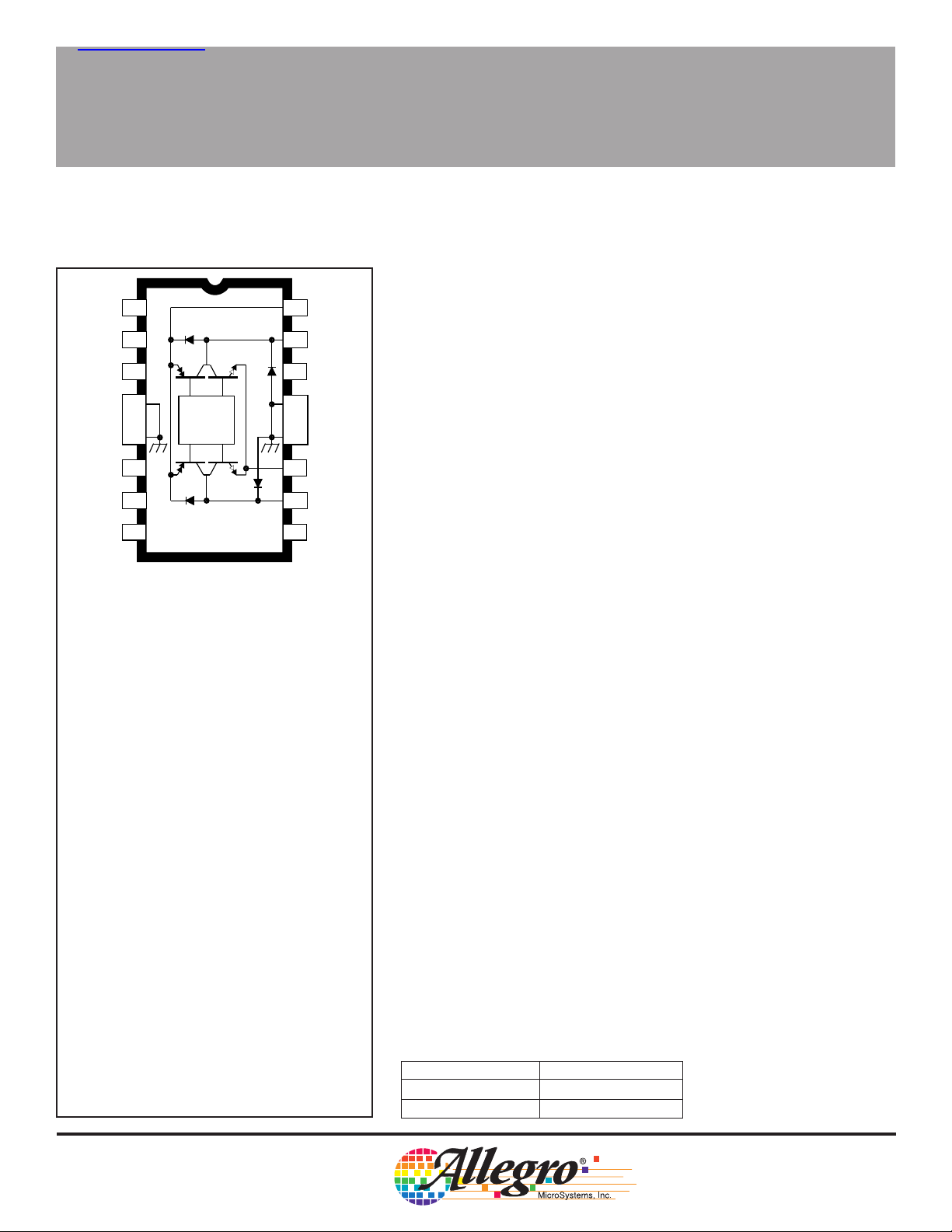
Note the A3955SB (DIP) and the A3955SLB
(SOIC) are electrically identical and share a
common terminal number assignment.
4
5
6
V
CC
7
D
8
2
LOGIC
V
BB
LOAD
16
SUPPLY
OUT
15
D
14
GROUND
13
12
GROUND
11
SENSE
OUT
10
9
D
Dwg. PP-056-2
Data Sheet
29319.41
3955
FULL-BRIDGE PWM
MICROSTEPPING MOTOR DRIVER
The A3955SB and A3955SLB are designed for driving one winding
of a bipolar stepper motor in a microstepping mode. The outputs are
rated for continuous output currents to ±1.5 A and operating voltages
B
0
A
1
to 50 V. Internal pulse-width modulated (PWM) current control combined with an internal three-bit nonlinear digital-to-analog converter
allows the motor current to be controlled in full-, half-, quarter-, or
eighth-step (microstepping) modes. Nonlinear increments minimize
the number of control lines necessary for microstepping.
Microstepping provides for increased step resolution, and reduces
torque variations and resonance problems at low speed.
Internal circuitry determines whether the PWM current-control
circuitry operates in a slow (recirculating) current-decay mode, fast
(regenerative) current-decay mode, or in a mixed current-decay mode
in which the off time is divided into a period of fast current decay with
the remainder of the fixed off time spent in slow current decay. The
combination of user-selectable current-sensing resistor and reference
voltage, digitally selected output current ratio; and slow, fast, or mixed
current-decay modes provides users with a broad, variable range of
motor control.
ABSOLUTE MAXIMUM RATINGS
Load Supply Voltage, VBB. . . . . . . . . . 50 V
Output Current, I
(Continuous) . . . . . . . . . . . . . . ±1.5 A*
Logic Supply Voltage, V
Logic/Reference Input Voltage Range,
V
. . . . . . . . . . . -0.3 V to VCC + 0.3 V
IN
Sense Voltage, V
Package Power Dissipation,
P
. . . . . . . . . . . . . . . . . . . . See Graph
D
Operating Temperature Range,
T
. . . . . . . . . . . . . . . . . -20˚C to +85˚C
A
Junction Temperature, T
Storage Temperature Range,
T
. . . . . . . . . . . . . . . . -55˚C to +150˚C
S
* Output current rating may be limited by duty
cycle, ambient temperature, and heat sinking.
Under any set of conditions, do not exceed the
specified current rating or a junction temperature
of 150˚C.
† Fault conditions that produce excessive junction
temperature will activate the device’s thermal
shutdown circuitry. These conditions can be
tolerated but should be avoided.
OUT
. . . . . . . . . 7.0 V
CC
. . . . . . . . . . . . . . . . 1.0 V
S
. . . . . . . +150˚C†
J
Internal circuit protection includes thermal shutdown with hysteresis, transient-suppression diodes, and crossover current protection.
Special power-up sequencing is not required.
The A3955S— is supplied in a choice of two power packages; a
16-pin dual-in-line plastic package with copper heat-sink tabs (suffix
‘B’), and a 16-lead plastic SOIC with copper heat-sink tabs (suffix ‘LB’).
For both package styles, the power tab is at ground potential and
needs no electrical isolation.
FEATURES
■ ±1.5 A Continuous Output Current
■ 50 V Output Voltage Rating
■ Internal PWM Current Control
■ 3-Bit Non-Linear DAC
■ Fast, Mixed Fast/Slow, and Slow Current-Decay Modes
■ Internal Transient-Suppression Diodes
■ Internal Thermal-Shutdown Circuitry
■ Crossover-Current and UVLO Protection
Always order by complete part number:
Part Number Package
A3955SB 16-Pin DIP
A3955SLB 16-Lead SOIC
3955
9
2814
6
7
16
10
15
1
4
5
11
12
13
3
FULL-BRIDGE PWM
MICROSTEPPING
MOTOR DRIVER
FUNCTIONAL BLOCK DIAGRAM
PHASE
GROUND
PFD
UVLO
& TSD
MIXED-DECAY
COMPARATOR
+
–
BLANKING
V
CC
R
T
PWM LATCH
R
Q
S
RC
C
T
LOGIC
SUPPLY
V
CC
BLANKING
GATE
+ –
A
OUT
V
BB
CURRENT-SENSE
COMPARATOR
÷3
V
TH
REF
D/A
2
D
B
OUT
LOAD
SUPPLY
SENSE
+
–
DISABLE
R
S
1
0
D
D
Table 1 — PHASE Truth Table
PHASE OUT
A
HH L
LL H
OUT
B
115 Northeast Cutoff, Box 15036
Worcester, Massachusetts 01615-0036 (508) 853-5000
W
Copyright © 1997 Allegro MicroSystems, Inc.
Table 2 — PFD Truth Table
V
PFD
≥3.5 V Slow Current-Decay Mode
1.1 V to 3.1 V Mixed Current-Decay Mode
≤0.8 V Fast Current-Decay Mode
Description
Dwg. FP-042

3955
FULL-BRIDGE PWM
MICROSTEPPING
MOTOR DRIVER
5
R = 6.0°C/W
θJT
4
D
2
Table 3 — DAC Truth Table
DAC DATA Current
D
D
1
0
Ratio, % V
REF/VS
H H H 100 3.00
3
2
SUFFIX 'B', R = 43°C/W
θJA
H H L 92.4 3.25
H L H 83.1 3.61
H L L 70.7 4.24
L H H 55.5 5.41
1
SUFFIX 'LB', R = 63°C/W
0
25
ALLOWABLE PACKAGE POWER DISSIPATION IN WATTS
50 75 100 125 150
θJA
TEMPERATURE IN °C
Dwg. GP-049-2A
L H L 38.2 7.85
L L H 19.5 15.38
L L L All Outputs Disabled
where VS = I
TRIP•RS
. See Applications section.
ELECTRICAL CHARACTERISTICS at TA = 25˚C, VBB = 5 V to 50 V, VCC = 4.5 V to 5.5 V
(unless otherwise noted.)
Limits
Characteristic Symbol Test Conditions Min. Typ. Max. Units
Power Outputs
Load Supply Voltage Range V
Output Leakage Current I
Output Saturation Voltage V
CE(SAT)
(Forward or Reverse Mode)
Sense Current Offset I
Clamp Diode Forward Voltage V
(Sink or Source)
Motor Supply Current I
(No Load)
BB(ON)
I
BB(OFF)
BB
CEX
SO
Operating, I
V
= V
OUT
V
= 0 V — <-1.0 -50 µA
OUT
= ±1.5 A, L = 3 mH V
OUT
BB
CC
—50 V
— <1.0 50 µA
VS = 1.0 V:
Source Driver, I
Source Driver, I
Sink Driver, I
Sink Driver, I
IS - I
OUT
, I
OUT
= 850 mA, 20 33 40 mA
= -0.85 A — 1.0 1.2 V
OUT
= -1.5 A — 1.3 1.5 V
OUT
= 0.85 A — 0.5 0.6 V
OUT
= 1.5 A — 1.3 1.5 V
OUT
VS = 0 V, VCC = 5 V
F
IF = 0.85 A — 1.2 1.4 V
I
= 1.5 A — 1.4 1.7 V
F
— 2.0 4.0 mA
D0 = D1 = D2 = 0.8 V — 1.0 50 µA
Continued next page…

3955
FULL-BRIDGE PWM
MICROSTEPPING
MOTOR DRIVER
ELECTRICAL CHARACTERISTICS at TA = 25˚C, VBB = 5 V to 50 V, VCC = 4.5 V to 5.5 V
(unless otherwise noted. )
Limits
Characteristic Symbol Test Conditions Min. Typ. Max. Units
Control Circuitry
Logic Supply Voltage Range V
Reference Voltage Range V
CC
REF
UVLO Enable Threshold VCC = 0 → 5 V 3.35 3.70 4.05 V
UVLO Hysteresis 0.30 0.45 0.60 V
Logic Supply Current I
Logic Input Voltage V
Logic Input Current I
Mixed-Decay Comparator V
CC(ON)
I
CC(OFF)
IN(1)
V
IN(0)
IN(1)
I
IN(0)
PFD
Trip Points
Mixed-Decay Comparator V
IO(PFD)
Input Offset Voltage
Mixed-Decay Comparator ∆V
IO(PFD)
Hysteresis
Reference Input Current I
Reference Divider Ratio V
REF
REF/VS
Digital-to-Analog Converter — 1.0 V < V
Accuracy*
Current-Sense Comparator V
IO(S)
Input Offset Voltage*
Operating 4.5 5.0 5.5 V
Operating 0.5 — 2.5 V
—4250mA
D0 = D1 = D2 = 0.8 V — 12 16 mA
2.0 — — V
— — 0.8 V
V
= 2.0 V — <1.0 20 µA
IN
V
= 0.8 V — <-2.0 -200 µA
IN
Slow Current-Decay Mode 3.5 — — V
Mixed Current-Decay Mode 1.1 — 3.1 V
Fast Current-Decay Mode — — 0.8 V
—0±20 mV
5.0 25 55 mV
V
= 0 V to 2.5 V — — ±5.0 µA
REF
at trip, D0 = D1 = D2 = 2 V — 3.0 — —
≤ 2.5 V — — ±3.0 %
REF
0.5 V < V
V
REF
≤ 1.0 V — — ±4.0 %
REF
= 0 V — — ±5.0 mV
Step Reference SRCR D
Current Ratio
* The total error for the V
function is the sum of the D/A error and the current-sense comparator input offset voltage.
REF/VS
= D1 = D2 = 0.8 V — 0 — %
0
D
= 2 V, D1 = D2 = 0.8 V — 19.5 — %
0
= 0.8 V, D1 = 2 V, D2 = 0.8 V — 38.2 — %
D
0
= D1 = 2 V, D2 = 0.8 V — 55.5 — %
D
0
= D1 = 0.8 V, D2 = 2 V — 70.7 — %
D
0
= 2 V, D1 = 0.8 V, D2 = 2 V — 83.1 — %
D
0
= 0.8 V, D1 = D2 = 2 V — 92.4 — %
D
0
D
= D1 = D2 = 2 V — 100 — %
0
Continued next page…
115 Northeast Cutoff, Box 15036
Worcester, Massachusetts 01615-0036 (508) 853-5000

3955
FULL-BRIDGE PWM
MICROSTEPPING
MOTOR DRIVER
ELECTRICAL CHARACTERISTICS at TA = 25˚C, VBB = 5 V to 50 V, VCC = 4.5 V to 5.5 V
(unless otherwise noted.)
Limits
Characteristic Symbol Test Conditions Min. Typ. Max. Units
Control Circuitry (cont’d)
Thermal Shutdown Temp. T
Thermal Shutdown Hysteresis ∆T
AC Timing
J
J
— 165 — °C
—15—°C
PWM RC Fixed Off-time t
PWM Turn-Off Time t
PWM Turn-On Time t
PWM Minimum On Time t
Crossover Dead Time t
OFF RC
PWM(OFF)
PWM(ON)
ON(min)
CODT
CT = 470 pF, RT= 43 kΩ 18.2 20.2 22.3 µs
Current-Sense Comparator Trip — 1.0 1.5 µs
to Source OFF, I
Current-Sense Comparator Trip — 1.4 2.5 µs
to Source OFF, I
IRC Charge ON to Source ON, — 0.4 0.7 µs
I
= 100 mA
OUT
Charge ON to Source ON, — 0.55 0.85 µs
I
RC
I
= 1.5 A
OUT
VCC = 5.0 V, RT ≥ 43 kΩ, CT = 470 pF 1.0 1.6 2.2 µs
I
= 100 mA
OUT
1 kΩ Load to 25 V 0.3 1.5 3.0 µs
= 100 mA
OUT
= 1.5 A
OUT

3955
FULL-BRIDGE PWM
MICROSTEPPING
MOTOR DRIVER
Terminal Functions
Terminal Name Description
1 PFD (Percent Fast Decay) The analog input used to set the current-decay mode.
2 REF (V
3 RC The parallel combination of external resistor RT and capacitor CT set the off time for the
4-5 GROUND Return for the logic supply (VCC) and load supply (VBB); the reference for all voltage
6 LOGIC SUPPLY (VCC) Supply voltage for the logic circuitry. Typically = 5 V.
7 PHASE The PHASE input determines the direction of current in the load.
8D2(DATA2) One-of-three (MSB) control bits for the internal digital-to-analog converter.
9D1(DATA1) One-of-three control bits for the internal digital-to-analog converter.
10 OUT
11 SENSE Connection to the sink-transistor emitters. Sense resistor RS is connected between this
12-13 GROUND Return for the logic supply (VCC) and load supply (VBB); the reference for all voltage
14 D
15 OUT
16 LOAD SUPPLY (VBB) Supply voltage for the load.
A
0
B
) The voltage at this input (along with the value of RS and the states of DAC inputs
REF
D0, D1, and D2) set the peak output current.
PWM current regulator. CT also sets the blanking time.
measurements.
One-of-two output load connections.
point and ground.
measurements.
(DATA0) One-of-three (LSB) control bits for the internal digital-to-analog converter.
One-of-two output load connections.
115 Northeast Cutoff, Box 15036
Worcester, Massachusetts 01615-0036 (508) 853-5000

3955
FULL-BRIDGE PWM
MICROSTEPPING
MOTOR DRIVER
Functional Description
Two A3955S— full-bridge PWM microstepping motor
drivers are needed to drive the windings of a bipolar
stepper motor. Internal pulse-width modulated (PWM)
control circuitry regulates each motor winding’s current.
The peak motor current is set by the value of an external
current-sense resistor (RS), a reference voltage (V
and the digital-to-analog converter (DAC) data inputs (D0,
D1, and D2).
To improve motor performance, especially when using
sinusoidal current profiles necessary for microstepping,
the A3955S— has three distinct current-decay modes:
slow decay, fast decay, and mixed decay.
PHASE Input. The PHASE input controls the direction of
current flow in the load (table 1). An internally generated
dead time of approximately 1 µs prevents crossover
currents that could occur when switching the PHASE
input.
DAC Data Inputs (D0, D1, D2). A non-linear DAC is used
to digitally control the output current. The output of the
DAC is used to set the trip point of the current-sense
comparator. Table 3 shows DAC output voltages for each
input condition. When D0, D1, and D2 are all logic low, all
of the power output transistors are turned off.
Internal PWM Current Control. Each motor driver
contains an internal fixed off-time PWM current-control
circuit that limits the load current to a desired value (I
Initially, a diagonal pair of source and sink transistors are
enabled and current flows through the motor winding and
V
BB
DRIVE CURRENT
RECIRCULATION
(SLOW-DECAY MODE)
RECIRCULATION
(FAST-DECAY MODE)
R
S
Dwg. EP-006-15
REF
),
TRIP
RS (figure 1). When the voltage across the sense resistor
equals the DAC output voltage the current-sense comparator resets the PWM latch, which turns off the source
drivers (slow-decay mode) or the sink and source drivers
(fast- or mixed-decay mode).
With the DATA input lines tied to VCC, the maximum
value of current limiting is set by the selection of RS and
V
with a transconductance function approximated by:
REF
I
≈ V
TRIP
The actual peak load current (I
than I
due to internal logic and switching delays. The
TRIP
/3RS.
REF
) will be slightly higher
PEAK
driver(s) remain off for a time period determined by a
user-selected external resistor-capacitor combination
(RTCT). At the end of the fixed off time, the driver(s) are
re-enabled, allowing the load current to increase to I
again, maintaining an average load current.
The DAC data input lines are used to provide up to
eight levels of output current. The internal 3-bit digital-toanalog converter reduces the reference input to the
current-sense comparator in precise steps (the step
reference current ratio or SRCR) to provide half-step,
quarter-step, or “microstepping” load-current levels.
I
≈ SRCR x V
TRIP
Slow Current-Decay Mode. When V
REF
/3R
S
≥ 3.5 V, the
PFD
device is in slow current-decay mode (the source drivers
are disabled when the load current reaches I
the fixed off time, the load inductance causes the current
).
to recirculate through the motor winding, sink driver,
ground clamp diode, and sense resistor (see figure 1).
Slow-decay mode produces low ripple current for a given
fixed off time (see figure 2). Low ripple current is desirable because the average current in the motor winding is
more nearly equal to the desired reference value, resulting in increased motor performance in microstepping
applications.
For a given level of ripple current, slow decay affords
the lowest PWM frequency, which reduces heating in the
motor and driver IC due to a corresponding decrease in
hysteretic core losses and switching losses respectively.
Slow decay also has the advantage that the PWM load
current regulation can follow a more rapidly increasing
reference before the PWM frequency drops into the
audible range. For these reasons slow-decay mode is
typically used as long as good current regulation can be
maintained.
). During
TRIP
TRIP
Figure 1 — Load-Current Paths

3955
FULL-BRIDGE PWM
MICROSTEPPING
MOTOR DRIVER
Under some circumstances slow-decay mode PWM
can fail to maintain good current regulation:
1) The load current will fail to regulate in slow-decay
mode due to a sufficiently negative back-EMF voltage
in conjunction with the low voltage drop across the
load during slow decay recirculation. The negative
back-EMF voltage can cause the load current to
actually increase during the slow decay off time. A
negative back-EMF voltage condition commonly
occurs when driving stepping motors because the
phase lead of the rotor typically causes the back-EMF
voltage to be negative towards the end of each step
(see figure 3A).
2) When the desired load current is decreased rapidly,
the slow rate of load current decay can prevent the
current from following the desired reference value.
A — Slow-Decay
3) When the desired load current is set to a very low
value, the current-control loop can fail to regulate due
to its minimum duty cycle, which is a function of the
user-selected value of t
pulse width t
that occurs each time the PWM
on(min)
and the minimum on-time
OFF
latch is reset.
Fast Current-Decay Mode. When V
≤ 0.8 V, the
PFD
device is in fast current-decay mode (both the sink and
source drivers are disabled when the load current reaches
I
). During the fixed off time, the load inductance
TRIP
causes the current to flow from ground to the load supply
via the motor winding, ground-clamp and flyback diodes
(see figure 1). Because the full motor supply voltage is
across the load during fast-decay recirculation, the rate of
load current decay is rapid, producing a high ripple current
for a given fixed off time (see figure 2). This rapid rate of
decay allows good current regulation to be maintained at
I
I
TRIP
PFD
PEAK
SLOW (V ≥ 3.5 V)
PFD
MIXED (1.1 V ≤ V ≤ 3.1 V)
FAST (V ≤ 0.8 V)
PFD
PFD
B — Fast-Decay
t
OFF
Figure 2 — Current-Decay Waveforms
C — Mixed-Decay
Dwg. WP-031-1
115 Northeast Cutoff, Box 15036
Worcester, Massachusetts 01615-0036 (508) 853-5000
Figure 3 — Sinusoidal Drive Currents

3955
FULL-BRIDGE PWM
MICROSTEPPING
MOTOR DRIVER
the cost of decreased average current accuracy or
increased driver and motor losses.
Mixed Current-Decay Mode. If V
is between 1.1 V
PFD
and 3.1 V, the device will be in a mixed current-decay
mode. Mixed-decay mode allows the user to achieve
good current regulation with a minimum amount of ripple
current and motor/driver losses by selecting the minimum
percentage of fast decay required for their application
(see also Stepper Motor Applications).
As in fast current-decay mode, mixed-decay starts with
the sink and source drivers disabled after the load current
reaches I
decays to a value below V
. When the voltage at the RC terminal
TRIP
, the sink drivers are re-
PFD
enabled, placing the device in slow current-decay mode
for the remainder of the fixed off time (figure 2). The
percentage of fast decay (PFD) is user determined by
V
or two external resistors.
PFD
PFD = 100 ln (0.6[R1+R2]/R2)
where
V
CC
R
1
PFD
R
2
With increasing values of t
switching losses will
OFF,
decrease, low-level load-current regulation will improve,
EMI will be reduced, the PWM frequency will decrease,
and ripple current will increase. A value of t
OFF
can be
chosen for optimization of these parameters. For applications where audible noise is a concern, typical values of
t
are chosen to be in the range of 15 µs to 35 µs.
OFF
RC Blanking. In addition to determining the fixed off-time
of the PWM control circuit, the CT component sets the
comparator blanking time. This function blanks the output
of the current-sense comparator when the outputs are
switched by the internal current-control circuitry (or by the
PHASE input, or when the device is enabled with the DAC
data inputs). The comparator output is blanked to prevent
false over-current detections due to reverse recovery
currents of the clamp diodes, and/or switching transients
related to distributed capacitance in the load.
During internal PWM operation, at the end of the t
OFF
time, the comparator’s output is blanked and CT begins to
be charged from approximately 0.22VCC by an internal
current source of approximately 1 mA. The comparator
output remains blanked until the voltage on CT reaches
approximately 0.6VCC. The blanking time, t
BLANK
, can be
calculated as:
t
= RTCT ln (RT/[RT - 3 kΩ]).
BLANK
Dwg. EP-062-1
Fixed Off-Time. The internal PWM current-control
circuitry uses a one shot to control the time the driver(s)
remain(s) off. The one-shot off-time, t
, is determined by
OFF
the selection of an external resistor (RT) and capacitor (CT)
connected from the RC timing terminal to ground. The offtime, over a range of values of CT = 470 pF to 1500 pF
and RT = 12 kΩ to 100 kΩ, is approximated by:
t
≈ RTCT.
OFF
When the load current is increasing, but has not yet
reached the sense-current comparator threshold (I
TRIP
),
the voltage on the RC terminal is approximately 0.6VCC.
When I
is reached, the PWM latch is reset by the
TRIP
current-sense comparator and the voltage on the RC
terminal will decay until it reaches approximately 0.22VCC.
The PWM latch is then set, thereby re-enabling the
driver(s) and allowing load current to increase again. The
PWM cycle repeats, maintaining the peak load current at
the desired value.
When a transition of the PHASE input occurs, CT is
discharged to near ground during the crossover delay time
(the crossover delay time is present to prevent simultaneous conduction of the source and sink drivers). After
the crossover delay, CT is charged by an internal current
source of approximately 1 mA. The comparator output
remains blanked until the voltage on CT reaches approximately 0.6VCC.
Similarly, when the device is disabled, via the DAC
data inputs, CT is discharged to near ground. When the
device is re-enabled, CT is charged by an internal current
source of approximately 1 mA. The comparator output
remains blanked until the voltage on CT reaches approximately 0.6VCC. The blanking time, t
, can be calcu-
BLANK
lated as:
t
= RTCT ln ([RT - 1.1 kΩ]/RT - 3 kΩ).
BLANK
The minimum recommended value for CT is 470 pF
± 5 %. This value ensures that the blanking time is
sufficient to avoid false trips of the comparator under

3955
FULL-BRIDGE PWM
MICROSTEPPING
MOTOR DRIVER
normal operating conditions. For optimal regulation of the
load current, this value for CT is recommended and the
value of RT can be sized to determine t
OFF
.
Thermal Considerations. Thermal-protection circuitry
turns off all output transistors when the junction temperature reaches approximately +165°C. This is intended only
to protect the device from failures due to excessive
junction temperatures and should not imply that output
short circuits are permitted. The output transistors are reenabled when the junction temperature cools to approximately +150°C.
V
BRIDGE A
V
PFD
V
REF
1
2
3
BB
16
+
47 µF
15
14
D
0A
Stepper Motor Applications. The A3955SB or
A3955SLB are used to optimize performance in
microstepping/sinusoidal stepper-motor drive applications
(see figures 4 and 5). When the load current is increasing, the slow current-decay mode is used to limit the
switching losses in the driver and iron losses in the motor.
This also improves the maximum rate at which the load
current can increase (as compared to fast decay) due to
the slow rate of decay during t
. When the load current
OFF
is decreasing, the mixed current-decay mode is used to
regulate the load current to the desired level. This prevents tailing of the current profile caused by the back-EMF
voltage of the stepper motor (see figure 3A).
BRIDGE B
D
1B
9
10
11
8
7
6
D
2B
PHASE
+5 V
B
+5 V
PHASE
470 pF
A
D
2A
4
30 kΩ
5
6
7
8
LOGIC
13
12
11
11
10
9
0.5 Ω
D
0B
47 µF
D
1A
V
BB
12
0.5 Ω
13
14
15
+
16
LOGIC
5
4
3
2
1
30 kΩ
470 pF
V
REF
V
PFD
Dwg. EP-047-3
Figure 4 — Typical Application
MIXED DECAY MIXED DECAYSLOW DECAY SLOW DECAY
Dwg. WK-004-3
Figure 5 — Microstepping/Sinusoidal Drive Current
115 Northeast Cutoff, Box 15036
Worcester, Massachusetts 01615-0036 (508) 853-5000

3955
FULL-BRIDGE PWM
MICROSTEPPING
MOTOR DRIVER
Table 4 — Step Sequencing
Bridge A Bridge B
Full Half Quarter Eighth
Step Step Step Step PHASEAD
1111 H H L L 70.7% H H L L 70.7%
2 H L H H 55.5% H H L H 83.1%
23 H L H L 38.2% H H H L 92.4%
4 H L L H 19.5% HHHH100%
235 XLLL 0% HHHH100%
6 L L L H -19.5% HHHH100%
4 7 L L H L -38.2% H H H L 92.4%
8 L L H H -55.5% H H L H 83.1%
2359 LHLL-70.7% H H L L 70.7%
10 L H L H -83.1% H L H H 55.5%
6 11 L H H L -92.4% H L H L 38.2%
12 L H H H -100% H L L H 19.5%
4 7 13 L H H H -100% X L L L 0%
14 L H H H -100% L L L H -19.5%
8 15 L H H L -92.4% L L H L -38.2%
16 L H L H -83.1% L L H H -55.5%
3 5 9 17 L H L L -70.7% L H L L -70.7%
18 L L H H -55.5% L H L H -83.1%
10 19 L L H L -38.2% L H H L -92.4%
20 L L L H -19.5% L H H H -100%
6 11 21 X L L L 0% L H H H -100%
22 H L L H 19.5% L H H H -100%
12 23 H L H L 38.2% L H H L -92.4%
24 H L H H 55.5% L H L H -83.1%
4 7 13 25 H H L L 70.7% L H L L -70.7%
26 H H L H 83.1% L L H H -55.5%
14 27 H H H L 92.4% L L H L -38.2%
28 H H H H 100% L L L H -19.5%
81529 H H H H 100% XLLL0%
30 H H H H 100% H L L H 19.5%
16 31 H H H L 92.4% H L H L 38.2%
32 H H L H 83.1% H L H H 55.5%
2A
D
1A
D
0A
I
LOADA
PHASEBD
2B
D
1B
D
0B
I
LOADB

3955
FULL-BRIDGE PWM
MICROSTEPPING
MOTOR DRIVER
A
100
92.4
83.1
70.7
55.5
38.2
CURRENT IN PER CENT
19.5
B
A
1/8 STEP
1/4 STEP
3/8 STEP
1/2 STEP
CURRENT IN PER CENT
MAXIMUM FULL-STEP
100% CONSTANT TORQUE
5/8 STEP
3/4 STEP
7/8 STEP
FULL STEP
Dwg. GK-020-1
TORQUE (141%)
B
10092.483.170.755.538.219.5
Figure 5 —
Current and Displacement Vectors
115 Northeast Cutoff, Box 15036
Worcester, Massachusetts 01615-0036 (508) 853-5000

3955
FULL-BRIDGE PWM
MICROSTEPPING
MOTOR DRIVER
This page intentionally left blank
3955
FULL-BRIDGE PWM
MICROSTEPPING
MOTOR DRIVER
16
0.280
0.240
A3955SB
Dimensions in Inches
(controlling dimensions)
NOTE 4
0.020
9
0.008
0.300
BSC
0.430
MAX
0.210
MAX
7.11
6.10
0.015
MIN
1
0.070
0.045
16
1
1.77
1.15
0.022
0.014
0.100
0.775
BSC
0.735
Dimensions in Millimeters
(for reference only)
NOTE 4
2.54
19.68
18.67
BSC
8
0.005
MIN
0.150
0.115
Dwg. MA-001-17A in
0.508
9
8
0.13
MIN
0.204
7.62
BSC
10.92
MAX
5.33
MAX
0.39
MIN
0.558
0.356
NOTES: 1. Exact body and lead configuration at vendor’s option within limits shown.
2. Lead spacing tolerance is non-cumulative
3. Lead thickness is measured at seating plane or below.
4. Webbed lead frame. Leads 4, 5, 12, and 13 are internally one piece.
115 Northeast Cutoff, Box 15036
Worcester, Massachusetts 01615-0036 (508) 853-5000
3.81
2.93
Dwg. MA-001-17A mm

3955
FULL-BRIDGE PWM
MICROSTEPPING
MOTOR DRIVER
A3955SLB
Dimensions in Inches
(for reference only)
0.2992
0.2914
0.020
0.013
0.0926
0.1043
16 9
1 2
3
0.4133
0.3977
0.0040
MIN.
Dimensions in Millimeters
(controlling dimensions)
16
0.0125
0.0091
0.419
0.394
0.050
0.016
0.050
BSC
9
0° TO 8°
Dwg. MA-008-17A in
0.32
0.23
7.60
7.40
0.51
0.33
2.65
2.35
1
0.10
2
MIN.
3
10.50
10.10
1.27
BSC
NOTES: 1. Exact body and lead configuration at vendor’s option within limits shown.
2. Lead spacing tolerance is non-cumulative
3. Webbed lead frame. Leads 4, 5, 12, and 13 are internally one piece.
10.65
10.00
0° TO 8°
1.27
0.40
Dwg. MA-008-17A mm

3955
FULL-BRIDGE PWM
MICROSTEPPING
MOTOR DRIVER
Allegro MicroSystems, Inc. reserves the right to make, from time to time, such
departures from the detail specifications as may be required to permit improvements in
the design of its products.
The information included herein is believed to be accurate and reliable. However,
Allegro MicroSystems, Inc. assumes no responsibility for its use; nor for any infringements of patents or other rights of third parties which may result from its use.
115 Northeast Cutoff, Box 15036
Worcester, Massachusetts 01615-0036 (508) 853-5000
 Loading...