

查询3951供应商
Data Sheet
29319.4†
3951
FULL-BRIDGE PWM MOTOR DRIVER
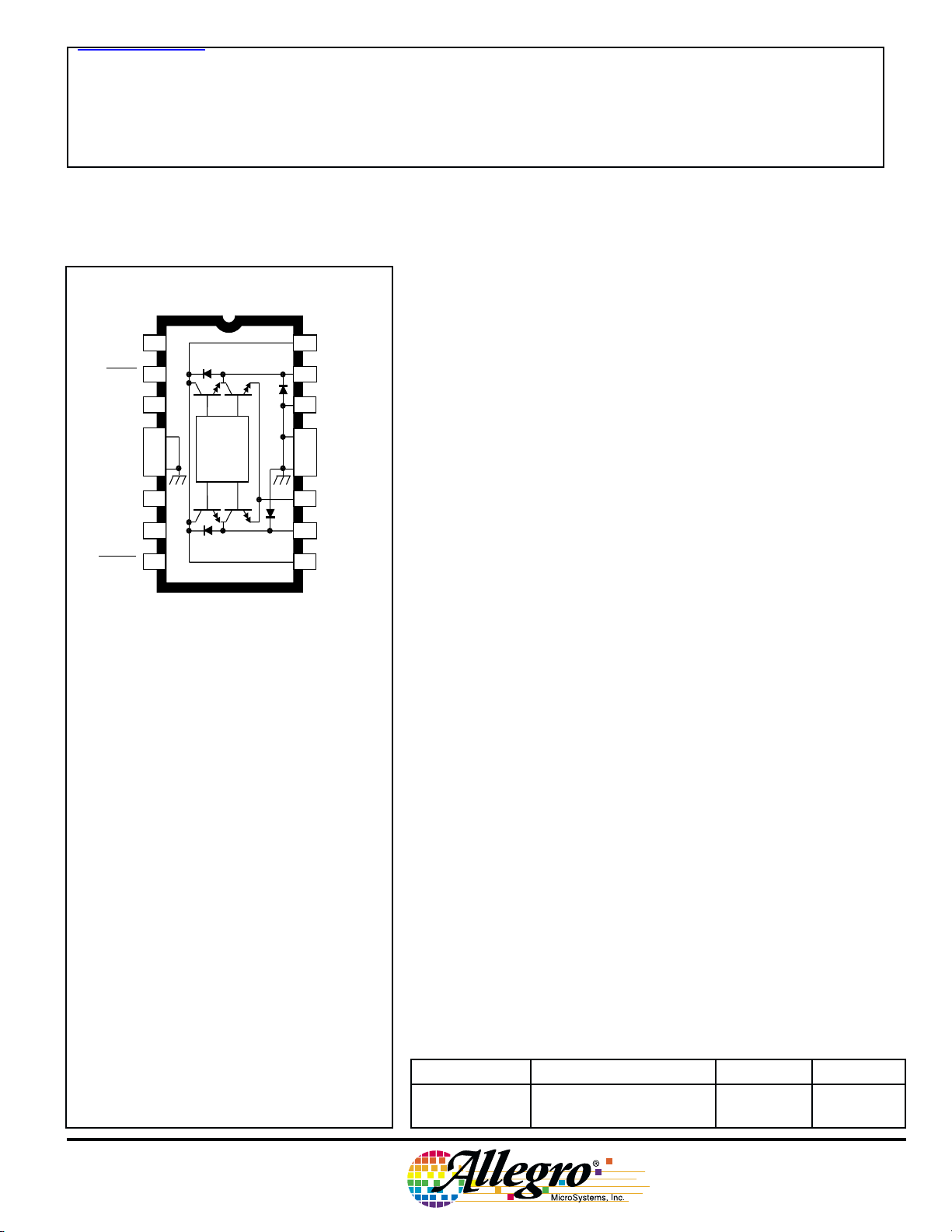
A3951SB
LOAD
1
REF/
BRAKE
GROUND
GROUND
LOGIC
SUPPLY
PHASE
ENABLE
NC
RC
2
3
4
5
6
V
CC
7
8
LOGIC
V
BB
V
BB
ABSOLUTE MAXIMUM RATINGS
Load Supply Voltage, V
Output Current, I
(tw ≤ 20 µs) .................................. ±3.5 A
(Continuous) ............................... ±2.0 A
Logic Supply Voltage, VCC.................. 7.0 V
Logic Input Voltage Range,
........................ -0.3 V to VCC + 0.3 V
V
IN
Sense Voltage, V
Reference Voltage, V
Package Power Dissipation,
PD ....................................... See Graph
Operating Temperature Range,
............................... –20°C to +85°C
T
A
Junction Temperature, TJ ............. +150°C*
Storage Temperature Range,
TS ............................. –55°C to +150°C
Output current rating may be limited by duty cycle,
ambient temperature, heat sinking and/or forced
cooling. Under any set of conditions, do not
exceed the specified current rating or a junction
temperature of +150°C.
* Fault conditions that produce excessive junction
temperature will activate device thermal shutdown
circuitry. These conditions can be tolerated but
should be avoided.
BB
OUT
........................ 1.5 V
SENSE
....................... V
REF
16
SUPPLY
15
OUT
B
14
GROUND
13
GROUND
12
GROUND
11
SENSE
10
OUT
A
LOAD
9
SUPPLY
Dwg. PP-056-1
................... 50 V
CC
Designed for bidirectional pulse-width modulated current control of
inductive loads, the A3951SB and A3951SW are capable of continuous
output currents to ±2 A and operating voltages to 50 V. Internal fixed
off-time PWM current-control circuitry can be used to regulate the
maximum load current to a desired value. The peak load current limit is
set by the user’s selection of an input reference voltage and external
sensing resistor. The fixed off-time pulse duration is set by a userselected external RC timing network. Internal circuit protection includes
thermal shutdown with hysteresis, transient suppression diodes, and
crossover-current protection. Special power-up sequencing is not
required. The A3951SB and A3951SW are improved replacements for
the UDN2953B and UDN2954W, respectively. For new system designs, the A3952SB/SEB/SLB/SW are recommended.
With the ENABLE input held low, the PHASE input controls load
current polarity by selecting the appropriate source and sink driver pair.
A user-selectable blanking window prevents false triggering of the PWM
current control circuitry. With the ENABLE input held high, all output
drivers are disabled.
When a logic low is applied to the BRAKE input, the braking
function is enabled. This overrides ENABLE and PHASE to turn off
both source drivers and turn on both sink drivers. The brake function
can be safely used to dynamically brake brush dc motors.
The A3951SB is supplied in a 16-pin dual in-line plastic package
with copper heat-sink contact tabs. The lead configuration enables
easy attachment of a heat sink while fitting a standard printed wiring
board layout. The A3951SW, for higher package power dissipation
requirements, is supplied in a 12-pin single in-line power-tab package.
In either package style, the batwing/power tab is at ground potential
and needs no isolation.
FEATURES
■ ±2 A Continuous Output Current Rating
■ 50 V Output Voltage Rating
■ Internal PWM Current Control
■ Internal Transient Suppression Diodes
■ Under-Voltage Lockout
■ Internal Thermal Shutdown Circuitry
■ Crossover-Current Protection
■ Default Brake Current Limit
Always order by complete part number:
Part Number Package R
θJA
A3951SB 16-Pin DIP 43°C/W 6.0°C/W
A3951SW 12-Pin Power-Tab SIP 36°C/W 2.0°C/W
R
θJT
3951
FULL-BRIDGE
PWM MOTOR DRIVER
FUNCTIONAL BLOCK DIAGRAM
ENABLE
REF/
GROUND
PHASE
BRAKE
9R
A
LOGIC
SUPPLY
CC
V
UVLO
& TSD
INPUT LOGIC
R
Q
1.5 V
R
BLANKING
V
CC
S
PWM LATCH
LOAD
SUPPLY
BB
V
+ –
OUT
V
TH
B
OUT
+
–
SENSE
RC
R
S
10
SUFFIX 'W',
R = 2.0°C/W
θJT
8
SUFFIX 'B',
R = 6.0°C/W
θJT
6
4
SUFFIX 'W', R = 38°C/W
2
SUFFIX 'B', R = 43°C/W
0
ALLOWABLE PACKAGE POWER DISSIPATION IN WATTS
25
θJA
50 75 100 125 150
TEMPERATURE IN °C
θJA
2
TRUTH TABLE
BRAKE ENABLE PHASE OUT
H H X Z Z Outputs Disabled
H L H H L Forward
H L L L H Reverse
L X X L L Brake, See Note
X = Irrelevant Z = High Impedance (source and sink both off)
NOTE: Includes internal default V
Dwg. GP-032A
115 Northeast Cutoff, Box 15036
Worcester, Massachusetts 01615-0036 (508) 853-5000
Copyright © 1994, 2000 Allegro MicroSystems, Inc.
OUTBDESCRIPTION
A
level for over-current protection.
sense
Dwg. FP-036-1
PWM MOTOR DRIVER
A3951SW
LOGIC
BB
V
CC
V
1 2 3 4 5 6 7 8 9 10 11 12
OUT
GROUND
B
LOAD
LOAD
SUPPLY
SUPPLY
BRAKE
REF/
RC
LOGIC
PHASE
SUPPLY
ENABLE
A
OUT
NC
Dwg. PP-058-1
3951
FULL-BRIDGE
SENSE
ELECTRICAL CHARACTERISTICS at TA = +25°C, VBB = 50 V, VCC = 5.0 V,
V
= 2.0 V, V
REF
Characteristic Symbol Test Conditions Min. Typ. Max. Units
Output Drivers
Load Supply Voltage Range V
Output Leakage Current I
Output Saturation Voltage V
Clamp Diode Forward Voltage V
(Source or Sink) IF = 1.0 A – 1.1 1.6 V
= 0 V, RC = 20 kΩ/1000 pF to Ground (unless noted otherwise).
SENSE
BB
CEX
CE(SAT)
F
Operating, I
V
= V
OUT
V
= 0 V – <-1.0 -50 µA
OUT
Source driver, I
Source driver, I
Source driver, I
Sink driver, I
Sink driver, I
Sink driver, I
IF = 0.5 A – 1.0 1.4 V
= ±2.0 A, L = 3 mH V
OUT
BB
= -0.5 A – 0.9 1.2 V
OUT
= -1.0 A – 1.0 1.4 V
OUT
= -2.0 A – 1.2 1.8 V
OUT
= +0.5 A – 0.9 1.2 V
OUT
= +1.0 A – 1.0 1.4 V
OUT
= +2.0 A – 1.3 1.8 V
OUT
Limits
CC
– 50 V
– <1.0 50 µA
Load Supply Current I
(No Load) I
I
www.allegromicro.com
BB(ON)
BB(OFF)
BB(BRAKE)
IF = 2.0 A – 1.4 2.0 V
V
V
V
= 0.8 V, V
ENABLE
= V
ENABLE
BRAKE
REF
= 0.8 V – 3.1 6.5 mA
= 2.0 V – 2.9 6.0 mA
REF
= 2.0 V – 3.1 6.5 mA
Continued next page …
3

3951
FULL-BRIDGE
PWM MOTOR DRIVER
ELECTRICAL CHARACTERISTICS (Continued)
Limits
Characteristic Symbol Test Conditions Min. Typ. Max. Units
Control Logic
Logic Supply Voltage Range V
Logic Input Voltage V
Logic Input Current I
Reference Voltage Range V
Reference Input Current I
V
IN(1)
I
IN(0)
REF
CC
IN(1)
IN(0)
REF
Reference Voltage Divider Ratio – V
PWM RC Fixed Off Time t
PWM Minimum On Time t
Propagation Delay Time t
off
on(min)
pd
Operating 4.5 5.0 5.5 V
2.0 ––V
––0.8 V
VIN = 2.0 V – <1.0 20 µA
VIN = 0.8 V – <-2.0 -200 µA
Operating 2.0 – V
2.0 V ≤ V
= 5 V 9.5 10.0 10.5 –
REF
REF
≤ V
CC
25 40 55 µA
CC
V
CT = 1000 pF, RT = 20 kΩ 18 20 22 µs
CT = 820 pF, RT ≥ 12 kΩ – 1.7 3.0 µs
CT = 1200 pF, RT ≥ 12 kΩ – 2.5 3.8 µs
I
= ±2.0 A, 50% EIN to 90% E
OUT
transition:
OUT
ENABLE on to source driver on – 2.9 – µs
ENABLE off to source driver off – 0.7 – µs
ENABLE on to sink driver on – 2.4 – µs
ENABLE off to sink driver off – 0.7 – µs
PHASE change to source driver on – 2.9 – µs
t
pd(pwm)
Thermal Shutdown Temperature T
Thermal Shutdown Hysteresis ∆T
UVLO Disable Threshold V
UVLO Hysteresis ∆V
Logic Supply Current I
(No Load) I
J
J
CC(UVLO)
CC(UVLO)
CC(ON)
CC(OFF)
I
CC(BRAKE)
NOTES: 1. Typical Data is for design information only.
2. Each driver is tested separately.
3. Negative current is defined as coming out of (sourcing) the specified device terminal.
4
PHASE change to source driver off – 0.7 – µs
PHASE change to sink driver on – 2.4 – µs
PHASE change to sink driver off – 0.7 – µs
Comparator trip to sink driver off – 0.8 1.5 µs
– 165 – °C
– 15 – °C
3.15 3.50 3.85 V
300 400 500 mV
V
V
V
= 0.8 V, V
ENABLE
= V
ENABLE
REF
115 Northeast Cutoff, Box 15036
Worcester, Massachusetts 01615-0036 (508) 853-5000
REF
= 0.8 V – 26 40 mA
= 2.0 V – 20 30 mA
REF
= 2.0 V – 12 18 mA

FUNCTIONAL DESCRIPTION
INTERNAL PWM CURRENT CONTROL DURING
FORWARD AND REVERSE OPERATION
The A3951SB/SW contain a fixed off-time pulse-width
modulated (PWM) current-control circuit that can be used
to limit the load current to a desired value. The value of
the current limiting (I
external current sensing resistor (RS) and reference input
voltage (V
). The internal circuitry compares the
REF
voltage across the external sense resistor to one tenth the
voltage on the REF input terminal, resulting in a function
approximated by
In forward or reverse mode the current-control circuitry limits the load current. When the load current
reaches I
, the comparator resets a latch to turn off the
TRIP
selected sink driver. The load inductance causes the
current to recirculate through the source driver and
flyback diode (two-quadrant operation or slow decay).
See figure 1.
) is set by the selection of an
TRIP
I
TRIP
= V
/(10•RS).
REF
V
BB
3951
FULL-BRIDGE
PWM MOTOR DRIVER
ENABLE
I
TRIP
LOAD
CURRENT
Figure 2 — Load-Current Waveform
INTERNAL PWM CURRENT CONTROL DURING
BRAKE MODE OPERATION
The brake circuit turns off both source drivers and
turns on both sink drivers. For dc motor applications, this
has the effect of shorting the motor’s back-EMF voltage,
resulting in current flow that brakes the motor dynamically.
However, if the back-EMF voltage is large and there is no
PWM current limiting, then the load current can increase to
a value that approaches a locked rotor condition. To limit
the current, when the I
level is reached, the PWM
TRIP
circuit disables the conducting sink driver. The energy
stored in the motor’s inductance is then discharged into
the load supply causing the motor current to decay.
RC
Dwg. WP-015-3
S
DRIVE CURRENT
RECIRCULATION
Dwg. EP-006-9
R
Figure 1 — Load-Current Paths
The user selects an external resistor (RT) and capaci-
tor (CT) to determine the time period (t
= RT•CT) during
off
which the drivers remain disabled (see “RC Fixed OFF
Time” below). At the end of the RTCT interval, the drivers
are re-enabled allowing the load current to increase again.
The PWM cycle repeats, maintaining the load current at
the desired value (see figure 2).
www.allegromicro.com
As in the case of forward/reverse operation, the drivers
are re-enabled after a time given by t
= RT•CT (see “RC
off
Fixed Off Time” below). Depending on the back-EMF
voltage (proportional to the motor’s decreasing speed), the
load current again may increase to I
. If so, the PWM
TRIP
cycle will repeat, limiting the load current to the desired
value.
Brake Operation
During braking, the peak current limit defaults internally to a value approximated by
I
= 1.5 V/RS.
TRIP
In this mode, the value of RS determines the I
independent of V
. This is useful in applications with
REF
TRIP
value
differing run and brake currents and no practical method of
varying V
REF
.
5

3951
FULL-BRIDGE
PWM MOTOR DRIVER
Choosing a small value for RS essentially disables the
current limiting during braking. Therefore, care should be
taken to ensure that the motor’s current does not exceed
the absolute maximum ratings of the device.
current can be measured by using an oscilloscope with a
current probe connected to one of the motor’s leads.
CAUTION: Because the kinetic energy stored in the
motor and load inertia is being converted into current,
which charges the VBB supply bulk capacitance (power
supply output and decoupling capacitance), care must be
taken to ensure the capacitance is sufficient to absorb the
energy without exceeding the voltage rating of any devices
connected to the motor supply.
RC Fixed Off Time
The internal PWM current control circuitry uses a one
shot to control the time the driver remains off. The one
shot time, t
of an external resistor (RT) and capacitor (CT) connected in
parallel from the RC terminal to ground. The fixed off time,
over a range of values of CT = 820 pF to 1500 pF and RT =
12 kΩ to 100 kΩ, is approximated by
When the PWM latch is reset by the current comparator, the voltage on the RC terminal will begin to decay from
approximately 3 volts. When the voltage on the RC
terminal reaches approximately 1.1 volts, the PWM latch is
set, thereby re-enabling the driver.
RC Blanking
In addition to determining the fixed off time of the
PWM control circuit, the CT component sets the comparator blanking time. This function blanks the output of the
comparator when the outputs are switched by the internal
current control circuitry (or by the PHASE, BRAKE, or
ENABLE inputs). The comparator output is blanked to
prevent false over-current detections due to reverse
recovery currents of the clamp diodes, and/or switching
transients related to distributed capacitance in the load.
During internal PWM operation, at the end of the off
time, the comparator’s output is blanked and CT begins to
be charged from approximately 1.1 V by an internal current
source of approximately 1 mA. The comparator output
remains blanked until the voltage on CT reaches approximately 3.0 volts.
(fixed off time), is determined by the selection
off
t
= RT•CT.
off
The braking
Similarly, when a transition of the PHASE input occurs,
CT is discharged to near ground during the crossover delay
time (the crossover delay time is present to prevent
simultaneous conduction of the source and sink drivers).
After the crossover delay, CT is charged by an internal
current source of approximately 1 mA. The comparator
output remains blanked until the voltage on CT reaches
approximately 3.0 volts.
Similarly, when the device is disabled via the ENABLE
input, CT is discharged to near ground. When the device is
re-enabled, CT is charged by the internal current source.
The comparator output remains blanked until the voltage
on CT reaches approximately 3.0 V.
For most applications, the minimum recommended
value is CT = 820 pF ±5 %. This value ensures that the
blanking time is sufficient to avoid false trips of the comparator under normal operating conditions. For optimal
regulation of the load current, the above value for CT is
recommended and the value of RT can be sized to determine t
regulation, see below.
LOAD CURRENT REGULATION WITH THE INTERNAL
PWM CURRENT-CONTROL CIRCUITRY
the range of PWM current control. This directly relates to
the limitations imposed by the V
100%) should utilize the A3952S–, which are recommended for the improvements they bring to new designs.
LOAD CURRENT REGULATION WITH EXTERNAL
PWM OF THE PHASE OR ENABLE INPUTS
modulated to regulate load current. Typical propagation
delays from the PHASE and ENABLE inputs to transitions
of the power outputs are specified in the electrical characteristics table. If the normal PWM current control is used,
then the comparator blanking function is active during
phase and enable transitions. This eliminates false
tripping of the over-current comparator caused by switching transients (see “RC Blanking” above).
. For more information regarding load current
off
During operation, the A3951S– have a lower limit to
input (2.0 V, minimum).
REF
Applications requiring a broader or full range (≈0% to
The PHASE or ENABLE inputs can be pulse-width
6
115 Northeast Cutoff, Box 15036
Worcester, Massachusetts 01615-0036 (508) 853-5000

V
BB
S
DRIVE CURRENT
RECIRCULATION
Dwg. EP-006-10
R
Figure 3 — Load-Current Paths
ENABLE Pulse-Width Modulation
Toggling the ENABLE input turns on and off the
selected source and sink drivers; the load inductance
causes the current to flow from ground to the load supply
via the ground clamp and flyback diodes (four-quadrant
operation or fast decay). See figure 3. When the device is
enabled, the internal current-control circuitry will be active
and can be used to limit the load current in the normal
internal PWM slow-decay or two-quadrant mode of operation.
3951
FULL-BRIDGE
PWM MOTOR DRIVER
between the duty cycle on the phase input and the average voltage applied to the motor is more linear than in the
case of ENABLE PWM control (which produces a discontinuous current at low current levels). See also, “DC Motor
Applications” below.
MISCELLANEOUS INFORMATION
An internally generated dead time prevents crossover
currents that can occur when switching phase or braking.
Thermal protection circuitry turns off all drivers should
the junction temperature reach 165°C (typical). This is
intended only to protect the device from failures due to
excessive junction temperatures and should not imply that
output short circuits are permitted. The hysteresis of the
thermal shutdown circuit is approximately 15°C.
If the internal current-control circuitry is not used; the
V
terminal should be connected to VCC, the SENSE
REF
terminal should be connected to ground, and the RC
terminal should be left floating (no connection).
An internal under-voltage lockout circuit prevents
simultaneous conduction of the outputs when the device is
powered up or powered down.
ENABLE
I
TRIP
LOAD
CURRENT
Dwg. WP-015-4
Figure 4 — ENABLE PWM Load-Current Waveform
PHASE Pulse-Width Modulation
Toggling the PHASE terminal determines/controls
which sink/source pair is enabled, producing a load current
that varies with the duty cycle and remains continuous at
all times. This can have added benefits in bidirectional
brush dc servo motor applications as the transfer function
www.allegromicro.com
APPLICATIONS NOTES
Current Sensing
The actual peak load current (I
than the calculated value of I
TRIP
off of the drivers. The amount of overshoot can be approximated as
I
OUTP
(VBB – ((I
≈
TRIP
• R
LOAD
L
where VBB is the load/motor supply voltage, V
back-EMF voltage of the load, R
resistance and inductance of the load respectively, and
t
is the propagation delay as specified in the electrical
pd(pwm)
characteristics table.
The reference terminal has an equivalent input resistance of 50 kΩ ±30%. This should be taken into account
when determining the impedance of the external circuit
that sets the reference voltage value.
) will be greater
OUTP
due to delays in the turn
) + V
LOAD
LOAD
BEMF
and L
)) • t
LOAD
pd(pwm)
is the
BEMF
are the
7

3951
FULL-BRIDGE
PWM MOTOR DRIVER
To minimize current-sensing inaccuracies caused by
ground trace I•R drops, the current-sensing resistor should
have a separate return to the ground terminal of the
device. For low-value sense resistors, the I•R drops in the
PCB can be significant and should be taken into account.
The use of sockets should be avoided as contact resistance can cause variations in the effective value of RS.
Larger values of RS reduce the aforementioned effects
but can result in excessive heating and power loss in the
sense resistor. The selected value of RS must not result in
the SENSE terminal absolute maximum voltage rating
being exceeded. The recommended value of RS is in the
range of
RS = (0.375 to 1.125)/I
TRIP
.
Thermal Considerations
For the most reliable operation, it is recommended that
the maximum junction temperature be kept as low as
practical, preferably below 125°C. The junction temperature can be measured by attaching a thermocouple to the
power tab/batwing of the device and measuring the tab
temperature, TT. The junction temperature then can be
approximated as
TJ ≈ TT + (2 • VF • I
OUT
• R
ΘJT
)
where VF is the clamp diode forward voltage and can be
determined from the electrical specification table for the
given level of I
. The value for R
OUT
is given in the
ΘJT
package thermal resistance table for the appropriate
package.
The power dissipation of the batwing package can be
improved by approximately 20% by adding a section of
printed circuit board copper (typically 6 to 18 square
centimeters) connected to the batwing terminals of the
device.
recommended) as close to the device as is physically
practical. To minimize the effect of system ground I•R
drops on the logic and reference input signals, the system
ground should have a low-resistance return to the load
supply voltage.
See also “Current Sensing” and “Thermal Consider-
ations” above.
Fixed Off-Time Selection
With increasing values of t
, switching losses de-
off
crease, low-level load-current regulation improves, EMI is
reduced, the PWM frequency will decrease, and ripple
current will increase. The value of t
can be chosen for
off
optimization of these parameters. For applications where
audible noise is a concern, typical values of t
are chosen
off
to be in the range of 15 to 35 µs.
DC Motor Applications
In closed-loop systems, the speed of a dc motor can
be controlled by PWM of the PHASE or ENABLE inputs, or
by varying the REF input voltage (V
). In digital systems
REF
(microprocessor controlled), PWM of the PHASE or
ENABLE input is used typically thus avoiding the need to
generate a variable analog voltage reference. In this case,
a dc voltage on the REF input is used typically to limit the
maximum load current.
In dc servo applications that require accurate positioning at low or zero speed, PWM of the PHASE input is
selected typically. This simplifies the servo-control loop
because the transfer function between the duty cycle on
the PHASE input and the average voltage applied to the
motor is more linear than in the case of ENABLE PWM
control (which produces a discontinuous current at lowcurrent levels).
The thermal performance in applications with high load
currents and/or high duty cycles can be improved by
adding external diodes in parallel with the internal diodes.
In internal PWM applications, only the two top-side
(flyback) diodes need be added. For external PHASE or
ENABLE input PWM applications, four external diodes
should be added for maximum junction temperature
reduction.
PCB Layout
The load supply terminal, VBB, should be decoupled
(>47 µF electrolytic and 0.1 µF ceramic capacitors are
8
115 Northeast Cutoff, Box 15036
Worcester, Massachusetts 01615-0036 (508) 853-5000
With bidirectional dc servo motors, the PHASE terminal can be used for mechanical direction control. Similar
to when braking the motor dynamically, abrupt changes in
the direction of a rotating motor produce a current generated by the back EMF. The current generated will depend
on the mode of operation. If the internal two-quadrant
slow-decay PWM current-control circuitry is used, the
maximum load current generated can be approximated by
I
LOAD
= V
BEMF/RLOAD
where V
is proportional to the
BEMF
motor’s speed. If external four-quadrant fast-decay
ENABLE PWM current-control is used, then the maximum
load current generated can be approximated by
I
LOAD
= (V
BEMF
+ VBB)/R
LOAD

For both cases, care must be taken to ensure that the
maximum current ratings of the device are not exceeded.
The load current will limit at a value
I
LOAD
= V
/(10•RS).
REF
CAUTION: When the direction of the motor is changed
abruptly, the kinetic energy stored in the motor and load
inertia will be converted into current that charges the V
BB
supply bulk capacitance (power supply output and
decoupling capacitance). Care must be taken to ensure
the capacitance is sufficient to absorb the energy without
exceeding the voltage rating of any devices connected to
the motor supply.
See also, the section on brake operation under
“Functional Description”, above.
Stepper Motor Applications
820 pF
PHASE
ENABLE
3951
FULL-BRIDGE
PWM MOTOR DRIVER
+5 V
1
2
BRAKE
3
25 kΩ
4
5
6
V
CC
7
8
LOGIC
V
BB
V
BB
V
BB
16
+
47 µF
15
14
13
12
11
10
9
0.5 Ω
Dwg. EP-047-1
The A3951SB and A3951SW may be used for
bidrectional control of bipolar stepper motors with continuous output currents to 2 A and peak start-up currents as
high as 3.5 A.
V
BB
12
11
10
LOGIC
9
8
V
CC
V
BB
7
6
5
4
3
2
1
ENABLE
PHASE
0.5 Ω
25 kΩ
V
REF1
1
1
820 pF
V
REF2
PHASE
ENABLE
25 kΩ
Typical DC Servo Motor Application
+5 V
47 µF
+
0.5 Ω
2
2
820 pF
1
2
V
3
4
5
6
7
8
9
10
11
12
BB
V
LOGIC
CC
www.allegromicro.com
Dwg. EP-048-1
Typical Bipolar Stepper Motor Application
9

3951
FULL-BRIDGE
PWM MOTOR DRIVER
16
0.280
0.240
A3951SB
Dimensions in Inches
(controlling dimensions)
NOTE 4
0.020
9
0.008
0.300
BSC
0.430
MAX
0.210
MAX
7.11
6.10
0.015
MIN
1
0.070
0.045
16
1.77
1.15
8
0.005
MIN
0.150
0.115
Dwg. MA-001-17A in
0.022
0.014
0.775
0.735
0.100
BSC
Dimensions in Millimeters
(for reference only)
0.508
NOTE 4
1
19.68
2.54
BSC
9
8
0.13
MIN
18.67
0.204
10.92
MAX
7.62
BSC
5.33
MAX
0.39
MIN
0.558
0.356
NOTES: 1. Leads 1, 8, 9, and 16 may be half leads at vendor’s option.
2. Lead thickness is measured at seating plane or below.
3. Lead spacing tolerance is non-cumulative.
4. Webbed lead frame. Leads indicated are internally one piece.
5. Exact body and lead configuration at vendor’s option within limits shown.
10
115 Northeast Cutoff, Box 15036
Worcester, Massachusetts 01615-0036 (508) 853-5000
3.81
2.93
Dwg. MA-001-17A mm

A3951SW
Dimensions in Inches
(controlling dimensions)
1.260
1.240
3951
FULL-BRIDGE
PWM MOTOR DRIVER
0.180
MAX
INDEX
AREA
0.065
0.035
0.020
0.51
0.775
0.765
0.245
0.225
0.155
0.145
ø
0.140
0.570
0.365
1
0.030
0.020
Dimensions in Millimeters
(for reference only)
12
0.100
±0.010
32.00
31.49
19.69
19.45
6.22
5.71
0.290
3.94
3.68
0.540
MIN
0.023
0.018
4.57
MAX
ø
0.055
0.045
0.135
0.100
0.080
0.070
Dwg. MP-007 in
1.40
1.14
INDEX
AREA
1.65
0.89
NOTES: 1. Lead thickness is measured at seating plane or below.
2. Lead spacing tolerance is non-cumulative.
3. Exact body and lead configuration at vendor’s option within limits shown.
4. Lead gauge plane is 0.030” (0.762 mm) below seating plane.
www.allegromicro.com
1
0.76
0.51
12
3.56
9.27
2.54
±0.254
14.48
13.71
7.36
MIN
0.59
0.45
3.43
2.54
2.03
1.77
Dwg. MP-007 mm
11

3951
FULL-BRIDGE
PWM MOTOR DRIVER
The products described here are manufactured under one or more
U.S. patents or U.S. patents pending.
Allegro MicroSystems, Inc. reserves the right to make, from time to
time, such departures from the detail specifications as may be required
to permit improvements in the performance, reliability, or
manufacturability of its products. Before placing an order, the user is
cautioned to verify that the information being relied upon is current.
Allegro products are not authorized for use as critical components
in life-support devices or systems without express written approval.
The information included herein is believed to be accurate and
reliable. However, Allegro MicroSystems, Inc. assumes no responsibility for its use; nor for any infringement of patents or other rights of
third parties which may result from its use.
12
115 Northeast Cutoff, Box 15036
Worcester, Massachusetts 01615-0036 (508) 853-5000
 Loading...