

1
2
3
4
7
0
5
6
7
8
9
8
5
6
1
2
3
4
7
0
5
6
7
8
9
8
5
6
查询A3940KLP-T供应商
FULL-BRIDGE POWER MOSFET CONTROLLER
1
2
3
1
2
2
2
3
2
4
2
5
2
2
6
2
7
8
2
9
2
10
1
11
1
12
1
1
13
1
14
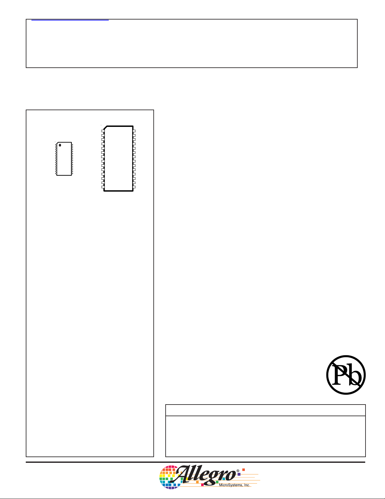
A3940KLP
(TSSOP with exposed
thermal pad)
4
5
6
7
8
9
10
11
12
13
14
A3940KLW
(SOIC)
29319.100i
Data Sheet
3940
— For Automotive Applications
The A3940KLP and A3940KLW are designed specifically for
automotive applications that require high-power motors. Each provides
2
2
2
2
2
2
2
2
2
1
1
1
1
1
four high-current gate drive outputs capable of driving a wide range of
n-channel power MOSFETs in a full-bridge configuration.
Bootstrap capacitors are utilized to provide the above-battery
supply voltage required for n-channel FETs. An internal charge pump
for the high side allows for dc (100% duty cycle) operation of the
bridge.
Protection features include supply under/overvoltage, thermal
shutdown, and motor lead short-to-battery and short-to-ground fault
notification, and a programmable dead-time adjustment for crossconduction prevention.
The overvoltage trip point is user adjustable.
Approx. 2X actual size.
ABSOLUTE MAXIMUM RATINGS
Load Supply Voltage Range, VBB,
VDRAIN, CP1 .......... -0.6 V to +40 V
Output Voltage Ranges,
LSS.............................. -2 V to +6.5 V
GHA/GHB, V
SA/SB, VSX.................. -2 V to +45 V
GLA/GLB, V
CA/CB, VCX.............. -0.6 V to +55 V
CP2,VCP, VIN.......... -0.6 V to +52 V
Logic Input/Output Voltage Range
VIN, V
................... -0.3 V to +6.5 V
OUT
Operating Temperature Range,
TA........................... -40°C to +135°C
Junction Temperature, TJ......... +150°C*
Storage Temperature Range,
TS........................... -55°C to +150°C
* Fault conditions that produce excessive
junction temperature will activate device
thermal shutdown circuitry. These conditions
can be tolerated, but should be avoided.
........ -2 V to +55 V
GHX
.......... -2 V to +16 V
GLX
The A3940 is supplied in a choice of two power packages, a 28-pin
TSSOP with an exposed thermal pad (package type LP), and a 28-pin
wide-body SOIC (package type LW). Both package types are available
in lead (Pb) free versions, with 100 % matte-tin leadframe plating
(suffix –T).
FEATURES
Drives wide range of n-channel MOSFETs
Charge pump to boost gate drive at low-battery-input conditions
Bootstrapped gate drive with charge pump for 100% duty cycle
Synchronous rectification
Fault diagnostic output
Adjustable dead-time cross-conduction protection
Motor lead short-to-battery and short-to-ground protection
Undervoltage/overvoltage protection
-40°C to +150°C, T
Thermal shutdown
Always order by complete part number
Part Number Pb-free Package
A3940KLP-T Yes 28-pin TSSOP
A3940KLP – 28-pin TSSOP
A3940KLW-T Yes 28-pin SOICW
A3940KLW – 28-pin SOICW
operation
J
3940
FULL-BRIDGE POWER
MOSFET CONTROLLER
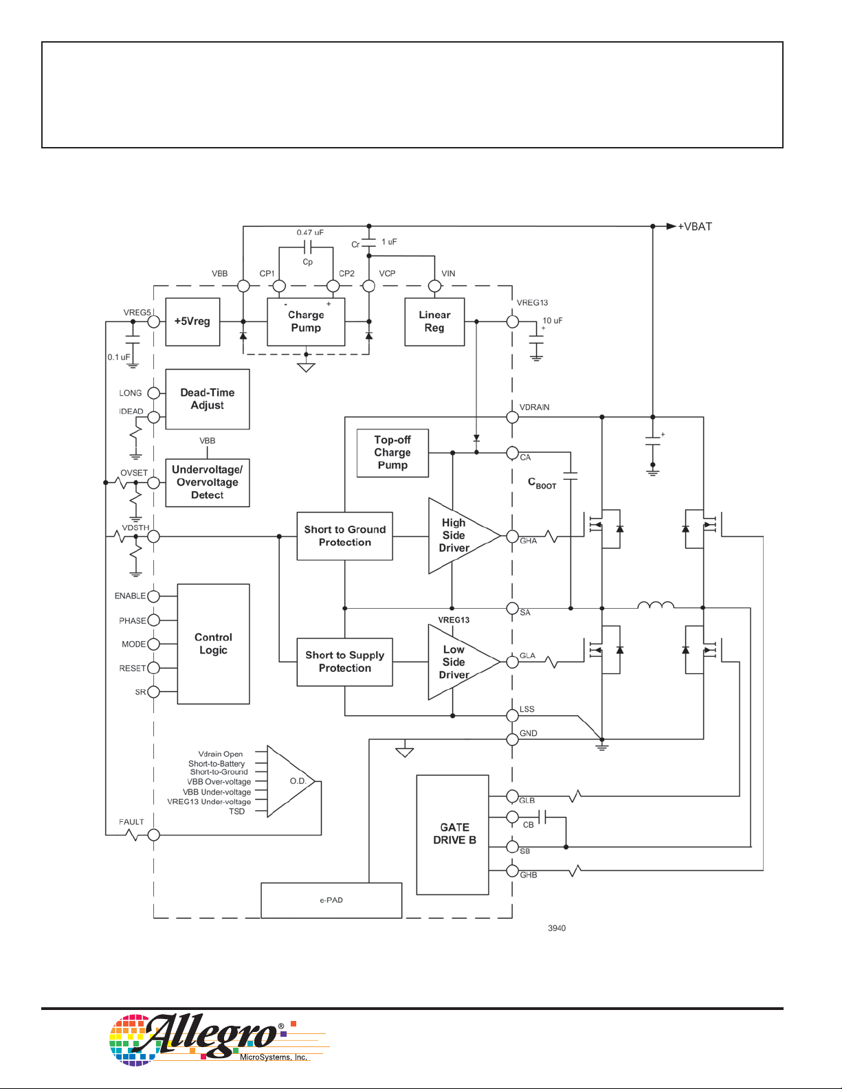
Functional Block Diagram
See pages 7 and 8 for terminal assignments and descriptions.
2
115 Northeast Cutoff, Box 15036
Worcester, Massachusetts 01615-0036 (508) 853-5000
Copyright © 2003 Allegro MicroSystems, Inc.
3940
FULL-BRIDGE POWER
MOSFET CONTROLLER
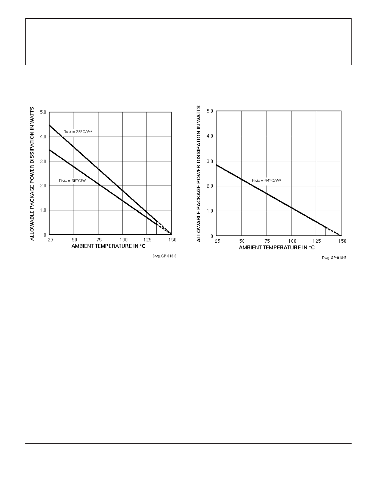
A3940KLW (SOIC)A3940KLP (TSSOP)
* Measured on “High-K” multi-layer PWB per JEDEC Standard JESD51-7.
† Measured on typical two-sided PWB .
The products described here are manufactured under one or more
U.S. patents or U.S. patents pending.
Allegro MicroSystems, Inc. reserves the right to make, from time to
time, such departures from the detail specifications as may be required
to permit improvements in the performance, reliability, or
manufacturability of its products. Before placing an order, the user is
cautioned to verify that the information being relied upon is current.
Allegro products are not authorized for use as critical components
in life-support devices or systems without express written approval.
The information included herein is believed to be accurate and
reliable. However, Allegro MicroSystems, Inc. assumes no responsibility for its use; nor for any infringement of patents or other rights of
third parties which may result from its use.
www.allegromicro.com
3
3940
FULL-BRIDGE POWER
MOSFET CONTROLLER
ELECTRICAL CHARACTERISTICS: unless otherwise noted at T
≤≤
VIN
≤ V
= 7 V to 40 V, Cp = 0.47 µF, Cr = 1 µF, C
≤≤
BB
= 0.1 µF, C
REG5
= -40°C to +135°C, TJ = -40°C to +150°C,
A
REG13
= 10 µF, C
= 0.1 µF, PWM = 22.5 kHz
BOOT
square wave.
Limits
Characteristics Symbol Conditions Min Typ Max Units
Power Supply
V
Quiescent Current I
BB
VREG5 Output Voltage V
VREG5 Line Regulation V
VREG5 Load Regulation V
VREG5 Short-Circuit Current I
VCP Output Voltage Level V
VCP Gate Drive I
VCP Output Voltage Ripple V
VCP Pump-Up time t
VREG13 Quiescent Input Current I
VREG13 Output Voltage V
VREG13 Dropout Voltage V
VREG13 Line Regulation V
VREG13 Load Regulation V
VREG13 Short-Circuit Current I
Go-to-Sleep Response Time t
Wake-Up Response Time t
BB
REG5
REG5
REG5
REG5M
CP
CP
CP(PP)
up
REG13
REG13
REGDV
REG13
REG13
REG13M
sleep
wake
NOTES: Typical Data is for design information only.
Negative current is defined as coming out of (sourcing) the specified device terminal.
RESET = 1, V
coast, stopped, CP disabled, I
RESET = 1, V
coast, stopped, CP disabled, I
RESET = 1, V
stopped, I
RESET = 1, V
stopped, I
RESET = 1, V
stopped, I
RESET = 1, V
stopped, I
= V
BB
BB
BB
DEAD
BB
= 170 µA, ICP = 0 mA
DEAD
BB
DEAD
BB
= 170 µA, ICP = 15 mA
DEAD
= 40 V, VIN ≠ VCP, – 4.8 7.0 mA
IN
DEAD
= 170 µA
= VIN = 15 V, VIN ≠ VCP, – 4.3 7.0 mA
= 170 µA
DEAD
= V
= 40 V, VIN ≠ VCP, coast, – 5.0 7.0 mA
IN
= 170 µA, ICP = 0 mA
= V
= 15 V, VIN ≠ VCP, coast, – 4.8 7.0 mA
IN
= V
= 40 V, VIN ≠ VCP, coast, – 35.4 40.0 mA
IN
= 170 µA, ICP = 15 mA
= V
= 15 V, VIN ≠ VCP, coast, – 35.1 40.0 mA
IN
RESET = 0 – – 1.0 µA
No load 4.5 5.0 5.5 V
I
= 4.0 mA – 5.0 – mV
REG5
I
= 0 - 4.0 mA, VBB = 40 V – 5.0 – mV
REG5
VBB = 40 V, V
VBB = 14 - 40 V, ICP = 15 mA
V
= 7 V, ICP = 15 mA 11.7 13 13.8 V
BB
= 0 – 28 – mA
REG5
VBB+9.5 VBB+10.7 VBB+11.8
V
SR = 1, MODE = 0, ENABLE = PWM 15 – – mA
ICP = 15 mA, VBB = 14 V - 40 V – 500 – mV
VIN = VCP, VBB = 14 V - 40 V – 2.5 – ms
VIN = VCP, VBB = 7 V – 3.5 – ms
RESET = 1, V
V
= 15 V, no load 12.6 13.3 14.0 V
IN
I
= 15 mA, VIN = 11 V - 14 V – 0.7 – V
REG13
VIN = 15 V - 40 V, I
VIN = 40 V, I
VIN = 40 V, V
RESET = 0 to V
RESET = 1 to V
= V
BB
REG13
REG13
= 40 V, coast, stopped – 1.4 – mA
IN
= 15 mA – 2.0 – mV
REG13
= 0 - 15 mA – 2.0 – mV
= 0 (pulse) – 60 – mA
= 4 V 10 30 – µs
REG5
, UV cleared – 1.4 – ms
REG13
Continued next page …
4
115 Northeast Cutoff, Box 15036
Worcester, Massachusetts 01615-0036 (508) 853-5000

3940
FULL-BRIDGE POWER
MOSFET CONTROLLER
ELECTRICAL CHARACTERISTICS: unless otherwise noted at T
≤≤
VIN
≤ V
= 7 V to 40 V, Cp = 0.47 µF, Cr = 1 µF, C
≤≤
BB
= 0.1 µF, C
REG5
= -40°C to +135°C, TJ = -40°C to +150°C,
A
REG13
= 10 µF, C
= 0.1 µF, PWM = 22.5 kHz
BOOT
square wave.
Limits
Characteristics Symbol Conditions Min Typ Max Units
Control Logic
Logic Input Voltage V
Logic Input Current I
V
V
I
I
IN(1)
IN(1)
IN(0)
IN(1)
IN(0)
IN(0)
Gate Drives, GHx, GLx ( internal SOURCE or upper switch stages)
Output High Voltage V
Source Current (pulsed) I
Source ON Resistance r
Source Load Rise Time t
DSL(H)
xU
SDU(on)
r
Gate Drives, GHx, GLx ( internal SINK or lower switch stages)
Output Low Voltage V
Sink Current (pulsed) I
Sink ON Resistance r
Sink Load Fall Time t
DSL(L)
xL
DSL(on)
f
Gate Drives, GHx, GLx (General)
Propagation Delay t
Output Skew Time t
Dead Time t
pd
sk(o)
dead
(Shoot-Through Prevention) LONG = 0, R
Between GHx, GLx transitions LONG = 1, R
of same phase LONG = 1, R
NOTES: Typical Data is for design information only.
Negative current is defined as coming out of (sourcing) the specified device terminal.
HIGH level input (Logic 1), except RESET. 2.0 – – V
HIGH level input (Logic 1) for RESET 2.2 – – V
LOW level input (Logic 0) – – 0. 8 V
VIN = 2.0 V – 40 100 µA
VIN = 0.8 V, except RESET(0) – 16 40 µA
VIN = 0.8 V, RESET(0) – – 1.0 µA
GHx: I
GLx: IxU = -10 mA, V
V
V
= -10 mA, Vsx = 0
xU
= 0
lss
= 10 V, TJ = 25°C – 700 – mA
SDU
= 10 V, TJ = 135°C 400 – – m A
SDU
V
REG13
V
REG13
- 2.2
- 0.2
–
V
REG13
–
V
REG13
V
V
IxU = -150 mA, TJ = 25°C 4.0 – 13 Ω
IxU = -150 mA, TJ = 135°C 7.0 – 23 Ω
Measure V
, 20% to 80%, CL = 3300 pF – 90 – ns
DSL
GHx: IxL = 10 mA, Vsx = 0 – – 150 mV
GLx: IxL = 10 mA, V
V
= 10 V, TJ = 25°C – 800 – mA
DSL
V
= 10 V, TJ = 135°C 550 – – mA
DSL
I
= +150 mA, TJ = 25°C 1.8 – 6.0 Ω
xL
I
= +150 mA, TJ = 135°C 3.0 – 7.5 Ω
xL
Measure V
DSL
= 0 – – 150 mV
lss
, 80% to 20%, CL = 3300 pF – 70 – ns
Logic input to unloaded GHx, GLx – – 225 ns
Grouped by rising or falling edge – – 50 ns
LONG = 0, R
= 12.1 kΩ (I
DEAD
= 499 kΩ (I
DEAD
= 12.1 kΩ (I
DEAD
= 499 kΩ (I
DEAD
= 167 µA) 0.3 – – µs
DEAD
= 4 µA) – – 11.0 µs
DEAD
= 167 µA) 8.3 – – µs
DEAD
= 4 µA) – – 345 µs
DEAD
For GH
: V
X
= VCX – V
SDU
For GL
: V
X
www.allegromicro.com
SDU
GHX
= V
, V
REG
DSL
= V
– V
GHX
GLX
– VSX, V
, V
DSL
= V
DSL(H)
GLX
= VCX – V
– V
LSS
, V
DSL(H)
SDU
– VSX.
= V
REG
– V
SDU
– V
LSS.
Continued next page …
5

3940
FULL-BRIDGE POWER
MOSFET CONTROLLER
ELECTRICAL CHARACTERISTICS: unless otherwise noted at T
≤≤
VIN
≤ V
= 7 V to 40 V, Cp = 0.47 µF, Cr = 1 µF, C
≤≤
BB
= 0.1 µF, C
REG5
= -40°C to +135°C, TJ = -40°C to +150°C,
A
REG13
= 10 µF, C
= 0.1 µF, PWM = 22.5 kHz
BOOT
square wave.
Limits
Characteristics Symbol Conditions Min Typ Max Units
Bootstrap Circuit
Diode Forward Current Limit I
Diode Forward Drop V
Diode Resistance R
CX
F
F
Top-off CP Source Current at Cx Icx VCX - VSX = 8 V, VBB = 40 V, GHx = 1(no load) 40 – – µA
Fault Logic
VBB Undervoltage V
VBB Undervoltage Hysteresis ∆V
VREG13 Undervoltage V
VREG13 Undervoltage Hyst.
VBB Overvoltage V
VBB Overvoltage Hysteresis ∆V
OVSET Input Current I
VDSTH Input Current I
Short-to-Ground Threshold V
Short-to-Battery Threshold V
V
/Open Bridge Threshold V
DRAIN
V
/Open Bridge Current I
DRAIN
y
Fault Latch Clear Pulsewidth t
Fault Clear Propagation Delay t
Fault Detection Noise Filter t
Fault Output V
Thermal Shutdown Temperature T
BB(uv)
BB(uv)
REG13(uv)
∆V
REG13(uv)VREG13(recovery)
BB(ov)
BB(ov)
SET(ov)
DSTH
STG(th)
STB(th)
DO(th)
VDRAIN
latch
pd
noise
out(0)
I
out(1)
J
Thermal Shutdown Hysteresis ∆T
NOTES: Typical Data is for design information only.
Negative current is defined as coming out of (sourcing) the specified device terminal.
3 V < [(V
= 13.5 V) - VCX] < 12 V 140 – 1000 mA
REG13
IF = 10 mA 0.8 – 2.0 V
RF(100) = [VF(150) - V
Decreasing V
V
BB(recovery)
Decreasing V
- V
BB
BB(uv)
IN
- V
Increasing VBB, FAULT = 0 to 1, V
Increasing VBB, FAULT = 0 to 1, V
Increasing VBB, FAULT = 0 to 1, V
V
- V
BB(ov)
0 V < V
0.3 V < V
V
DSTH
V
DSTH
V
DSTH
V
DSTH
V
DSTH
V
DSTH
If V
DRAIN
BB(recovery)
< 0.9 V – – 1.4 µA
SET(ov)
< 3 V – – 1.0 µA
DSTH
= 0.3 V
= 1.0 V
= 3.0 V
= 0.3 V
= 1.0 V
= 3.0 V
< V
DO(th)
(50)]/100 1.5 – 6.5 Ω
F
4.5 5.25 6.0 V
200 450 700 mV
7.5 8.25 9.0 V
REG13(uv)
= 0 V 16 19.6 22 V
OVSET
= 0.45 V 24 28 30.5 V
OVSET
= 0.9 V 32.5 36.4 39 V
OVSET
200 450 700 mV
2.1 3.1 4.1 V
V
-0.14 – V
DSTH
V
-0.18 – V
DSTH
V
-0.39 – V
DSTH
V
-0.20 – V
DSTH
V
-0.24 – V
DSTH
V
-0.37 – V
DSTH
, FAULT = 0 to 1 1.0 – 3.0 V
RESET = 0 – – 1.0 µA
RESET = 1, V
< 3 V – – 500 µA
DSTH
RESET = 0, pulse 0.15 – 2.0 µs
From RESET = 1 to FAULT = 0 – 2.0 – µs
– 1.7 – µs
I
= 5 mA, faults negated – – 0.4 V
out
V
= 5 V, open-drain, fault asserted – – 1.0 µA
out
TJ increasing – 172 – °C
TJ decreasing – 12 – °C
J
DSTH
DSTH
DSTH
DSTH
DSTH
DSTH
+0.10
+0.13
+0.26
+0.30
+0.30
+0.30
V
V
V
V
V
V
6
115 Northeast Cutoff, Box 15036
Worcester, Massachusetts 01615-0036 (508) 853-5000

3940
FULL-BRIDGE POWER
MOSFET CONTROLLER
Terminal Functions
Terminal
Terminal Name Function Number
VDRAIN Kelvin connection to MOSFET high-side drains 1
LSS Gate-drive source return, low-side 2
GLB Gate-drive B output, low-side 3
SB Motor phase B input 4
GHB Gate-drive B output, high-side 5
CB Bootstrap capacitor B 6
VIN Regulated 13 V gate drive supply input 7
VREG13 Regulated 13 V gate drive supply output 8
CA Bootstrap A capacitor 9
GHA Gate-drive A output, high-side 10
SA Motor phase A input 11
GLA Gate-drive A output, low-side 12
VBB Battery supply 13
CP2 Charge pump connection for pumping capacitor 14
VCP Charge pump output 15
CP1 Charge pump connection for pumping capacitor 16
GND Common ground and dc supply returns
Electrically connected to exposed thermal pad of LP package 17
FAULT Open-drain fault output 18
OVSET DC input, overvoltage threshold setting for V
VREG5 Regulated 5 V supply output 20
MODE Control input 21
SR Control input 22
ENABLE Control input 23
PHASE Control input 24
RESET Control input 25
LONG Control input, long or short deadtime 26
IDEAD Adjust current for basic deadtime 27
VDSTH DC input, drain-to-source monitor threshold voltage 28
BB
19
www.allegromicro.com
7

3940
FULL-BRIDGE POWER
MOSFET CONTROLLER
Terminal Descriptions
CA/CB. High-side connection for bootstrap capacitor, positive
supply for high-side gate drive. The bootstrap capacitor is
charged to V
– 1.5 V when the output Sx terminal is low.
REG13
When the output swings high, the voltage on this terminal rises
with the output to provide the boosted gate voltage needed for nchannel power MOSFETs.
RESET. Control input to put device into minimum power
consumption mode and to clear latched faults. Logic “1”
enables the device; logic “0” triggers the sleep mode. Internally
pulled down via 50 kΩ resistor.
ENABLE. Logic “1” enables direct control of the output
drivers via the PHASE input, as in PWM controls, and ignores
the MODE and SR inputs. Internally pulled down via 50 kΩ
resistor.
MODE. Logic input to set the current decay mode. Logic “1”
(slow-decay mode) switches off the high-side MOSFET in
response to a PWM “off” command. Logic “0” (fast-decay
mode) switches off both the high-side and low-side MOSFETs.
Internally pulled down via 50 kΩ resistor.
PHASE. Motor direction control. When logic “1”, enables
gate drive outputs GHA and GLB allowing current flow from
SA to SB. When logic “0”, enables GHB and GLA allowing
current flow from SB to SA. Internally pulled down via 50 kΩ
resistor.
SR. When logic “1”, enables synchronous rectification; logic
“0” disables the synchronous rectification. Internally pulled
down via 50 kΩ resistor.
FAULT. Open drain, diagnostic logic output signal. When
logic “1”, indicates that one or more fault conditions have
occurred. Use an external pullup resistor to VREG5 or to digital
controller. Internally causes a coast when asserted. See also
Functional Description, next page.
GLA/GLB. Low-side gate drive outputs for external, n-channel
MOSFET drivers. External series gate resistors can control slew
rate seen at the power driver gate.
GND. Common ground and dc supply returns. Exposed
thermal pad of LP package is NOT internally connected to
GND.
LSS. Low-side gate drivers’ return. Connects to the common
sources in the low-side of the power MOSFET bridge. It is the
reference connection for the short-to-battery monitor.
OVSET. A positive, dc level that controls the VBB overvoltage
trip point. Usually, provided from precision resistor divider
network between V
V
, sets unspecified but high overvoltage trip point, effec-
REG5
and GND. If connected directly to
REG5
tively eliminating the overvoltage protection.
SA/SB. Directly connected to the motor terminals, these
terminals sense the voltages switched across the load and are
connected to the negative side of the bootstrap capacitors. Also,
are the negative supply connection for the floating, high-side
drivers.
VBB. Positive supply voltage. Usually connected to the motor
voltage supply. If VBB is above a specified level or below a
specified level, a fault will be asserted.
VDRAIN. Kelvin connection for drain-to-source voltage (shortto-ground) monitor and is connected to high-side drains of the
MOSFET bridge. Also used to detect “open drain”.
VDSTH. A positive, dc level that sets the short-to-ground and
short-to-battery monitor threshold voltage. If the drain-source
voltage exceeds this level (after the dead time) during an “on”
state, a fault will be asserted.
CP1 [CP2]. Charge pump capacitor negative [positive] side. If
not using the charge pump, leave both terminals open.
IDEAD. Analog current set by resistor (12 kΩ<R
DEAD
<500 kΩ)
to ground. In conjunction with LONG, determines dead time
between GHx and GLx transitions of same phase. V
IDEAD
= 2 V.
LONG. When logic “1”, selects long dead time between GHx
and GLx transitions of same phase. When logic “0”, selects
short dead times. Internally pulled down via 50 kΩ resistor.
GHA/GHB. High-side gate-drive outputs for n-channel
MOSFET drivers. External series gate resistors can control slew
rate seen at the power driver gate.
8
115 Northeast Cutoff, Box 15036
Worcester, Massachusetts 01615-0036 (508) 853-5000
VCP. Charge pump output for VREG13 input. If not using the
charge pump, connect this terminal to VBB.
VIN. Positive supply voltage for the V
linear regulator.
REG13
Usually connected to VCP, the charge-pump output gate drive.
If not using the charge pump, connect VIN to VBB or other dc
supply greater than 11 V.
VREG13. High-side, gate-driver supply. If V
REG13
falls below
a specified level, a fault will be asserted.
VREG5. Regulated 5 V output for internal logic.

Functional Description
3940
FULL-BRIDGE POWER
MOSFET CONTROLLER
Motor Lead Protection. A fault detection circuit monitors
the voltage across the drain to source of the external MOSFETs.
A fault is asserted “high” on the output terminal, FAULT, if the
drain-to-source voltage of any MOSFET that is instructed to turn
on is greater than the voltage applied to the V
When a high-side switch is turned on, the voltage from V
input terminal.
DSTH
DRAIN
to
the appropriate motor phase output, VSX, is examined. If the
motor lead is shorted to ground the measured voltage will
exceed the threshold and the FAULT terminal will go “high”.
Similarly, when a low-side MOSFET is turned on, the differential voltage between the motor phase (drain) and the LSS
terminal (source) is monitored. V
to V
REG5
.
is set by a resistor divider
DSTH
To prevent erroneous motor faults during switching, the
fault circuitry will wait two dead times after every PWM/phase
change before monitoring the drain-to-source voltage; except, it
will use one dead time for (1) a long coast to any phase on, or
(2) a long hi-Z before on for that phase. This allows time for the
motor output voltage to settle before checking for motor fault
when using slow rise/fall gate-control waveforms.
The V
is intended to be a Kelvin connection for the
DRAIN
high-side, drain-source monitor circuit. Voltage drops across
the power bus are eliminated by connecting an isolated PCB
trace from the V
bridge. This allows improved accuracy in setting the V
terminal to the drain of the MOSFET
DRAIN
DSTH
threshold voltage. The low-side, drain-source monitor uses the
LSS terminal, rather than V
, in comparing against V
DRAIN
DSTH
.
Fault States. The FAULT terminal provides real time
indication of fault conditions after some digital noise filtering.
The V
fault acts as if a short-to-ground fault existed on
DRAIN
every motor phase. Bridge (or motor) faults are latched but
cleared by a RESET = 0 pulse or by power cycling. GHx = GLx
= 0 during RESET = 0. The undervoltage, overvoltage, and
thermal shutdown faults are not latched and will not reset until
the cause is eliminated. All faults cause, via the FAULT line, a
coast and some cause shutdown of the regulators, as in the Fault
Responses table (next page).
Note: As a test mode, if the thermal shutdown or SLEEP has not
occurred and the FAULT output is externally held low, the coast
mode and regulator shutdowns will not occur if motor or voltage
faults occur. Do not wire-OR this terminal to other FAULT
lines.
Dead Time. The A3940 is intended to drive a wide range of
power MOSFETs in applications requiring a wide range of
switching times. In order to prevent cross conduction (a.k.a.
shoot-through) during direction and PWM changes, a power
MOSFET must be turned off before its “phase-pin mate” is
turned on.
(ns) = K([18.8R
t
DEAD
(kΩ)] + 50) + 90
DEAD
where K = 1 for LONG = 0; K = 32 for LONG = 1.
Note: I
(mA) ≈ 2/R
DEAD
(kΩ), 12 kΩ<R
DEAD
DEAD
<500 kΩ.
Sleep Mode. RESET = 0 clears any latched motor faults
while driving all gate drive outputs low (coast). Eventually,
RESET = 0 turns off all circuits to allow minimum current draw.
GHx and GLx outputs go high impedance (Z) when V
REG13
<
4 V. RESET = 1 enables the device after it powers up all
circuits. The user should wait the pump-up time, t
, to allow the
up
device to be powered up properly before a gate output is
enabled. Please refer to power-up diagram in application note
AN295040 for more detail.
Charge Pump. The A3940 is designed to accommodate a
wide range of power supply voltages. The charge pump output
voltage, VCP, is regulated to VBB + 11 V (or about 2VBB if
VBB < 11 V).
VREG13. A 13.3 V, low-dropout, linear regulator is used to
power the low-side gate drive circuit directly and to provide the
current to charge the bootstrap capacitors for the high-side gate
drive. The input supply connection to this regulator, VIN, can
be externally connected to the charge pump output, VCP, or it
can be directly connected to the VBB or VBAT terminal.
Internal current limiting protects V
REG13
.
VREG5. A 5 V, low-dropout, linear regulator is used to power
the internal logic, regulators, and thermal detection. This
regulator can also power low-current external resistor networks
for VDSTH and OVSET, and the FAULT output pull-up. The
input supply connection is VBB. Internal current limiting
protects V
REG5
.
Power-Up State. If the input logic is open, internal pulldowns put the system in coast mode on powering up. First, issue
a brake command for >10 µs to charge the bootstrap capacitors
and avoid a possible short-to-ground fault indication.
www.allegromicro.com
9

3940
FULL-BRIDGE POWER
MOSFET CONTROLLER
Functional Description (cont’d)
Control Logic
PHASE ENABLE MODE
SR GLA GLB GHA GHB SA SB Mode of Operation
0 1 X X 1 0 0 1 Lo Hi Reverse
0 0 0 1 0 1 1 0 Hi Lo Fast decay, SR enabled
0 0 1 1 1 1 0 0 Lo Lo Slow decay, braking mode
0 0 0 0 0 0 0 0 Z Z Fast decay, coast
0 0 1 0 1 0 0 0 Lo Z Slow decay, SR disabled
1 1 X X 0 1 1 0 Hi Lo Forward
1 0 0 1 1 0 0 1 Lo Hi Fast decay, SR enabled
1 0 1 1 1 1 0 0 Lo Lo Slow decay, braking mode
1 0 0 0 0 0 0 0 Z Z Fast decay, coast
1 0 1 0 0 1 0 0 Z Lo Slow decay, SR disabled
NOTES: All faults will coast the motor, i.e., GHA = GHB = GLA = GLB = 0 to switch off all bridge MOSFETs.
X = Indicates a “don’t care”.
Z = Indicates a high-impedance state.
Fault Responses
Fault Mode RESET FAULT
CP Reg. VREG13 VREG5
GHx GLx
No Fault 1 0 ON ON ON – –
Short-to-Battery"# 1 1 ON ON ON 0 0
Short-to-Ground"$ 1 1 ON ON ON 0 0
Open Bridge (V
V
Undervoltage 1 1 ON ON& ON 0' 0'
REG13
)"% 1 1 ON ON ON 0 0
DRAIN
VBB Overvoltage 1 1 ON ON ON 0 0
VBB Undervoltage 1 1 OFF OFF ON& 0' 0'
Thermal Shutdown 1 1 OFF OFF ON& 0' 0'
Sleep 0 1 OFF OFF OFF Z Z
NOTES: " = These faults are latched but will clear during RESET = 0 pulse. GHx = GLx = 0 during RESET = 0, except see '.
Other faults will not clear except when their cause is removed.
# = Short-to-battery can only be detected when the corresponding GLx
= 1.
$ = Short-to-ground can only be detected when the corresponding GHx = 1.
% = Bridge fault appears as a short-to-ground fault on all motor phases.
& = Not instructed off but may be low voltage because of the fault indicated.
' = During undervoltage conditions, the low sides of GHx and GLx are instructed to be “on” so that the outputs are
low = 0; however, with V
10
< 4 V, the outputs will start to open (become high impedance). See “Sleep Mode”.
REG13
115 Northeast Cutoff, Box 15036
Worcester, Massachusetts 01615-0036 (508) 853-5000

A3940KLP (TSSOP)
3940
FULL-BRIDGE POWER
MOSFET CONTROLLER
Dimensions in Inches
(for reference only)
NOTES: 1. Exact body and lead configuration at vendor’s option within limits shown.
2. Lead spacing tolerance is non-cumulative.
3. Supplied in standard sticks/tubes of 50 devices or add “TR” to part number for tape and reel.
www.allegromicro.com
Dimensions in Millimeters
(controlling dimensions)
11

3940
FULL-BRIDGE POWER
MOSFET CONTROLLER
A3940KLW (SOIC)
Dimensions in Inches
(for reference only)
NOTES: 1. Lead spacing tolerance is non-cumulative.
2. Exact body and lead configuration at vendor’s option within limits shown.
3. Supplied in standard sticks/tubes of 27 devices or add “TR” to part number for tape and reel.
12
Dimensions in Millimeters
(controlling dimensions)
115 Northeast Cutoff, Box 15036
Worcester, Massachusetts 01615-0036 (508) 853-5000

 Loading...