

E
查询3936供应商
3936
DMOS THREE-PHAS
ABSOLUTE MAXIMUM RATINGS
at TA = +25°C
Load Supply Voltage, VBB........................... 50 V
Output Current, I
Logic Supply Voltage, VDD......................... 7.0 V
Logic Input Voltage Range, VIN
(tW>30 ns) .......... -0.3 V to V
(tW<30 ns) ................ -1.0V to VDD +1V
Sense Voltage, V
Reference Voltage, V
Package Power Dissipation,
P
Operating Temperature Range,
T
Junction Temperature, TJ......................... +150°C
Storage Temperature Range,
T
* Output current rating may be limited by duty cycle,
ambient temperature, and heat sinking. Under any set of
conditions, do not exceed the specified current rating or a
junction temperature of 150°C.
D
A
S
................................... ±3 A*
OUT
+ 0.3 V
DD
................................. 0.5 V
SENSE
................................ VDD
REF
............................................... 3.9 W
................................ -20°C to +85°C
............................... -55°C to +150°C
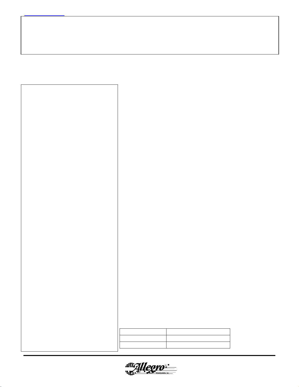
PWM MOTOR DRIVER
Designed for pulse-width modulated (PWM) current control of threephase brushless dc motors, the A3936SED is capable of peak output currents
to ± 3 A and operating voltages to 50 V. Internal fixed off-time PWM currentcontrol timing circuitry can be configured to operate in slow-, fast- and mixeddecay modes.
Internal synchronous rectification control circuitry is provided to
improve power dissipation during PWM operation.
Internal circuit protection includes thermal shutdown with
hysteresis, and crossover current protection. Special power up sequencing is
not required.
The A3936 is supplied in a 44-pin plastic PLCC with a copper
batwing tabs (suffix ‘ED’). The power tabs are at ground potential and need
no electrical isolation. This device is also available in a lead-free version
(100% matte tin leadframe).
Features
±3 A, 50 V Continuous Output Rating
Low
Configurable Mixed, Fast and Slow Current-Decay Modes
Synchronous Rectification for Low Power Dissipation
Internal UVLO and Thermal Shutdown Circuitry
Crossover-Current Protection
Tachometer Output for External Speed Control Loop
Always order by complete part number
Part Number Package
A3936SED 44-pin PLCC
A3936SED-T 44-pin PLCC, Lead-free
r
Outputs (typically 500 mΩ source, 315 mΩ sink)
DS(on)
A3936-DS Rev. 1

3936 Three Phase PWM Motor Driver
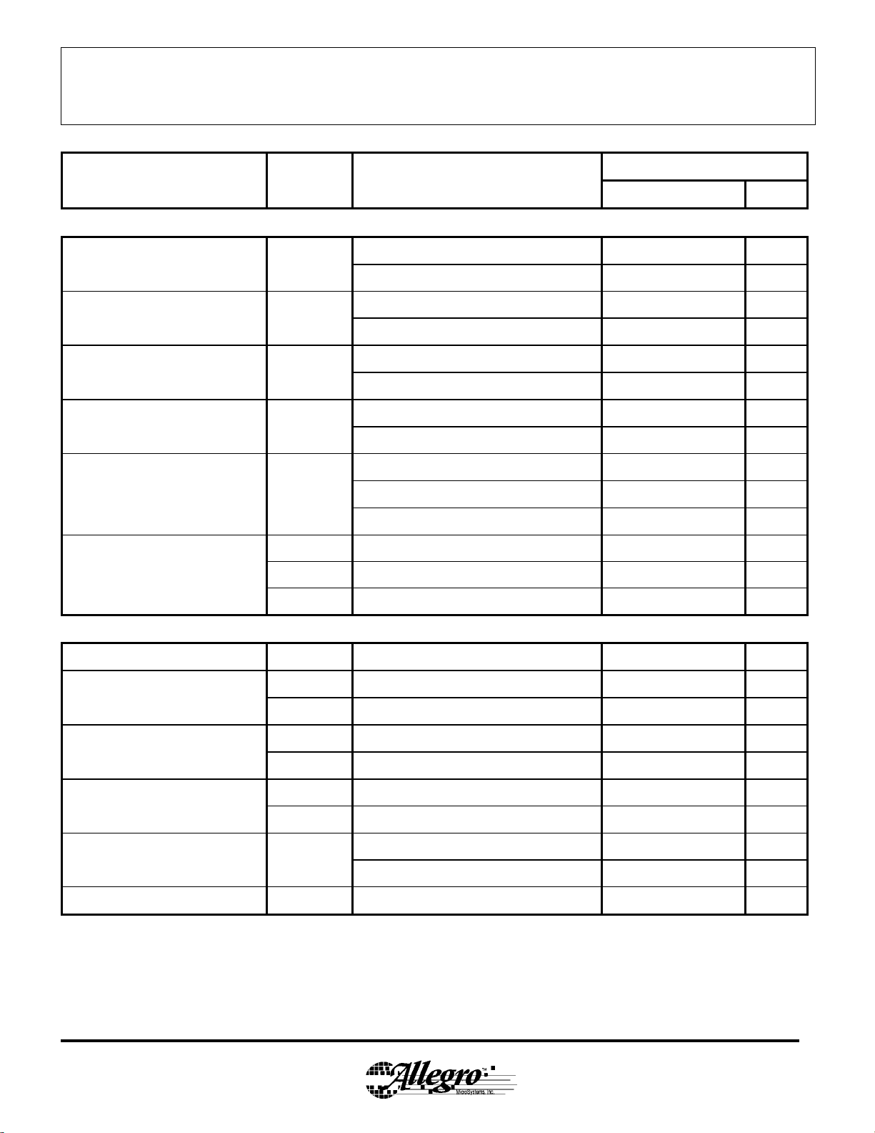
FUNCTIONAL BLOCK DIAGRAM
.22uf/100V
.22uf/50V
VREG
V
DD
REGULATOR CHARGE PUMP
CP2
CP1
VCP
HALL
HALL
HALL
TACH
HBIAS
HA+
HB+
HC+
SLEEP
DIR
EXTMODE
BRAKE
ENABLE
HA-
HB-
HC-
SR
Comm
Logic
Control
Logic
BANDGAP
GATE
DRIVE
OVERVOLTAGE
UNDERVOLTAGE
AND FAULT
DETECT
VCPVREG
ZERO
DETECT
+-
CURRENT
VBB1
VBB2
OUTA
OUTB
OUTC
LSS2
LSS1
SENSE
R
GND
.22uf/50V
.1uF
S
VDD
BLANK
OSC
PFD1
PFD2
PWM
TIMER
+-
SENSE
CURRENT
BUFFER/
DIVIDER
REF
3936 Three Phase PWM Motor Driver
ELECTRICAL CHARACTERISTICS at TJ= +25°C, VBB = 50 V, VDD=5.0V,f
< 50KHz (unless noted otherwise)
PWM
Limits
Characteristics Symbol Test Conditions Min. Typ. Max. Units
Output Drivers
Load SupplyVoltage Range VBB Operating 9 – 50 V
During Sleep Mode 0 50 V
Output Leakage Current I
Output On Resistance R
BodyDiodeForward Voltage V
Motor Supply Current I
Logic Supply Current
DSS
DSON
F
BB
I
DD
V
OUT=VBB
V
= 0 V – <–1.0 -20 µA
OUT
SourceDriver, I
Sink Driver, I
= -3A – .55 Ω
OUT
=3A – .35 Ω
OUT
–<1.020 µA
Source Diode, IF= -3A – – 1.4 V
Sink Diode, IF=3A – – 1.3 V
f
<50kHz – 4 7 mA
PWM
Charge Pump On, Outputs Disabled – 2 5 mA
Sleep Mode – – 20 uA
f
<50kHz – 10 mA
PWM
Control Logic
Logic Supply Voltage Range V
Logic Input Voltage V
Logic Input Current I
(except ENABLE) I
Logic Input Current I
ENABLE Input I
Outputs Off – 8 mA
Sleep Mode (Inputs belo w.5V) 100 µA
DD
IN(1)
V
IN(0)
IN(1)
IN(0)
IN(1)
IN(0)
OSC
Operating 3 5.0 5.5 V
VDD*.5 – – V
––V
*.2 V
DD
VIN=VDD*.5 -20 <1.0 20 µA
VIN=VDD*.2 -20 <-1.0 20 µA
VIN=VDD*.5 – 100 µA
VIN=VDD*.2 – 30 µA
OSC shorted to GND 3 4 5 MHzInternalOscillator f
R
= 51K 3.4 4 4.6 MHz
OSC

3936 Three Phase PWM Motor Driver
ELECTRICAL CHARACTERISTICS at TJ= +25°C, VBB=50V,VDD= 5.0 V, f
< 50KHz (unless noted
PWM
otherwise)
Limits
Characteristics Symbol Test Conditions Min. Typ. Max. Units
Control Logic
Buffer Input Offset Volt. V
V
Input Voltage Range Operating 0.0 – V
REF
Reference Input Current I
Comparato rInput Offset Volt. V
IO
REF
IO
ERR
(Note3)
V
REF=VDD,VBB
V
=0V ±5 mV
REF
V
REF=VDD
=.5V -14 14 %
V
REF
=0 to 50V -.5 0 0.5 µA
-4 4 %GMError V
Propagatio nDelay Times tpd 50% TO 90%, SR Enabled
PWM CHANGE TO SOURCE ON 600 750 1000 ns
PWM CHANGE TO SOURCE OFF 50 150 350 ns
PWM CHANGE TO SINK ON 600 750 1000 ns
PWM CHANGE TO SINK OFF 50 100 150 ns
±10 mV
DD
V
Crossover Delay t
Thermal Shutdown Temp. T
Thermal Shutdown Hysteresis ∆T
COD
J
J
UVLO EnableThresho ld Rising V
SR Enabled 300 600 1000 ns
– 165 – °C
–15– °C
DD
2.45 2.7 2.95 V
UVLO Hysteresis 0.05 0.10 – V
NOTES: 1. Typical Data is for design information only.
2. Negative current is defined as coming out of(sourcing) the specified device pin.
3.
V
=((V
ERR
REF
/10) – V
SENSE
)/(V
REF
/10)
3936 Three Phase PWM Motor Driver
ELECTRICAL CHARACTERISTICS at TA= +25°C, VBB=50V,VDD=5.0Vf
< 50KHz (unless noted
PWM
otherwise)
Limits
Characteristics Symbol Test Conditions Min. Typ. Max. Units
Hall Logic
Hall Input Current I
Common Mode Input Range VCMR .3 2.5 V
AC Input VoltageRange V
Hysteresis V
Pulse Reject Filter 35.58 µs
Hall Bias Output Sat Voltage V
Tach Output V
HALL
HALL
HYS
HB
I
HB
OL
VIN=1.2V -1 0 1 µA
.120 Vp-p
TA= -20 to 85 deg C. 10 30 mV
I
=40mA, TA= -20 to 85 deg C. .4 .5 V
OUT
40 mA
I
= 500uA .5 V
OUT
NOTES: 1. Typical Data is for design information only.
2. Negative current is defined as coming out of (sourcing) the specified devicepin.
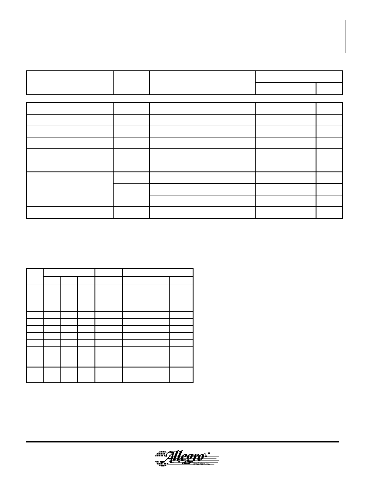
Commutation Truth Table
120 spacing
HA
HB HC DIR OUTA OUTB OUTC
1+-+FOR HI LO Z
2+-- FOR HI Z LO
3++- FOR Z HI LO
4-+-FOR LO HI Z
5-++FOR LO Z HI
6--+FOR Z LO HI
1+-+REV LO HI Z
2 + - - REV LO Z HI
3 + + - REV Z LO HI
4-+- REV HI LO Z
5-++REV HI Z LO
6 - - + REV Z HI LO
--- X Z Z Z
+++ X Z Z Z
Outputs

3936 Three Phase PWM Motor Driver
Functional Description
VREG. Th e VREG pin should be decoupled with a 0.22
µF capacitor to gr ound. This supplyvoltage is used to run
the sink side DMOS outputs. VREG is internally monitored
and in the case ofa fault condition, the outputs of the device
are disabled.
Charge Pump.The Charge Pump is used to generate a
supply above VBB to drive the source side DMOS gates. A
0.22 uF ceramic monolithic capacitor should be connected
between CP
and CP2for pumping purposes. A 0.22 uF
1
ceramic monolithic capacitor should beconnected between
V
and VBBto act as a reservoir to run the high side
CP
DMOS devices. The V
Voltageis internally monitored
CP
and in the case ofa fault condition the outputs of the device
are disabled.
Shutdown. In the event of a fault due to excessive
junction temperature, or lowvoltage on V
outputs of the device ar e disabled until the fault condition is
removed. At power up, and in the event of low V
UVLO circuit disables the drivers.
or V
CP
REG
DD
,the
,the
Current Regulation. Load current is regulated by an
internal fixed off time PWM control circuit. When the
outputs of the DMOS H-bridge are turned on, current
increases in the motor winding until it reaches a value given
by:
I
TRIP=VREF
At the trip point, the sensecomparator resets the source
enable latch, turning offthe source driver. At th is point,
load inductance causes the current to recirculate for the
fixed off time period. The current path during recirculation
is determined by the configuration of slow/mixed decay
mode and the synchronous rectification control setting.
/(10*R
SENSE
)
Extmode Logic. When using external PWM current
control, the EXTMODE input determines the current path
during the chopped cycle. With EXTMODE set low, fast
decaymode, both the source and sink drivers are chopped
OFF during the decaytime (ENABLE=0). With
EXTMODE high, slow decay mode, only the source driver
turns off during the current decay time.
EXTMODE Decay
0Fast
1Slow
Sleep Mode. The input pin SLEEP is dedicated to put
the device into a minimum current draw mode. When
asserted low, all circuits are disabled.
Fixed Off-Time. The 3936 is set for a fixed off time of
96 counts of the intern al oscillator, typically24 µs with
4Mhz oscillator.
Internal Current Control Mode. Input pins PFD1
and PFD2 determine the current decay method after an
overcurrent event is detected at sense input. In slow decay
mode both sink side drivers are turned on for the fixed off
time period. Mixed decaymode starts out in fast decay
mode for the selected percentage of the fixed off time, and
then is followed by slow decay for the rest of the period.
PFD2 PFD1 % t
OFF
00 0Slow
0 1 15 Mixed
1 0 48 Mixed
1 1 100 Fast
Decay
Enable Logic. The Enable input terminal allows
external PWM. ENABLE high turns ON the selected sinksourcepair, enable low switches offthe appropriate drivers
and the load current decays. Ifthe ENABLEpin is held
high, the current will rise until it reaches the level set by the
internal current control circuit.
ENABLE Outputs
0 Source
Chopped
1ON

3936 Three Phase PWM Motor Driver
PWM Blank Timer. When a sourcedriver turnson, a
current spikeoccurs due to the reverserecovery currents of
the clamp diodes and/or switching transients related to
distributed capacitance in the load. To prevent this current
spike from erroneouslyresetting the source enable latch, the
sense comparator is blanked. The blank timer run s after the
offtime counter to provide the blanking function. The blank
timer is reset when ENABLE is chopped or DIRis changed.
For external PWM control, a DIR change or ENABLE ON
will trigger the blanking function. The duration is adjusted
by control input BLANK.
BLANK t
06/f
1 12/f
BLANK
OSC
OSC
Brake. Logic high to the brake terminal activates the
brake function, logic low allows normal operation. Brake
will turn all three sink dr ivers ON and effectively shorts out
the motor generated BEMF. It is important to note th at the
internal PWM current control circuit will not limit the
current when braking, sincethe current does not flow
through the sense resistor. Themaximum current can be
approximated by V
BEMF/RL
that the maximum ratings of the device ar e not exceeded in
worse case braking situations of h igh speed an d high
inertial loads.
. Care should be taken to insure
Synchronous Rectification. Logic high applied to
the SR terminal enables synchronous rectification. When a
PWM off cycle is triggered, either by an ENABLE chop
command or internal fixed off time cycle, load current will
recirculate according to the decay mode selected by control
logic. The A3936 synchronous rectification feature will turn
on the appropriate MOSFET(s)during the current decay and
effectivelyshort out the bodydiodes with the lowRdson
driver. This will lower power dissipation significantly and
can eliminate the need for external schottky diodes.
Reversal of load current is prevented by turning off
synchronous rectification when a zero current level is
detected.
Oscillator. The PWMtimer is based on an internal
oscillator set by a resistor connected from the OSC terminal
to V
. Typical value of 4Mhz is set with 51k resistor.
DD
F
OSC
= 204E9/R
OSC
.
Tach. A tachometer signal is available for speed
measurement. This open collector output toggles at each
Hall transition.

3936
Terminal List
Pin No. Pin Name Pin Description
1GND
2GND
3 HA+ Hall input
4 HA- Hall input
5 HB+ Hall input
6 HB- Hall input
7 HC+ Hall input
8 HC- Hall input
9V
10 REF GmReference Input Voltage
11 GND
12 GND
13 GND
14 BRAKE Logic Input
15 SENSE Sense Resistor Connection
16 SR Logic Input (Disabled = Low, Active SR = High)
17 OUTA DMOS H – Bridge A
18 HBIAS Connection for hall element neg side
19 VBB1 Load Supply Voltage
20 LSS1 Low Side Source connection
21 OUTB DMOS H – Bridge B
22 GND
23 GND
24 GND
25 LSS2 Low Side Source connection
26 VBB2 Load Supply Voltage
27 TACH Speed output
28 OUTC DMOS H – Bridge C
29 V
30 CP1 Charge Pump Capacitor Terminal
31 CP2 Charge Pump Capacitor Terminal
32 SLEEP Logic input for SLEEP mode
33 GND
34 GND
35 GND
36 OSC Oscillator Terminal
37 V
38 DIR Logic Input
39 ENABLE Logic Input
40 EXTMODE Logic Input
41 BLANK Logic Input
42 PFD2 Logic Input
43 PFD1 Logic Input
44 GND Power Ground Tab
DD
CP
REG
Logic Supply Voltage
Reservoir Capacitor Terminal
Regulator decoupling Terminal

3936
 Loading...