

查询3935供应商
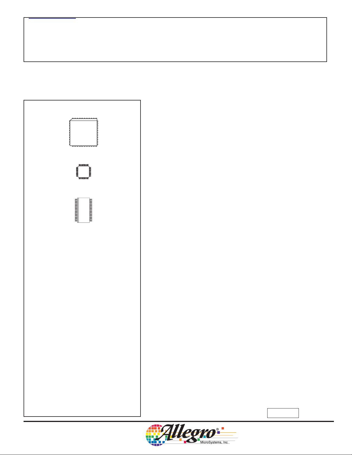
Package ED, 44-Pin PLCC
Package JP, 48-Pin LQFP
Package LQ, 36-Pin SOIC
26301.102b
3935
3-PHASE POWER MOSFET CONTROLLER
— For Automotive Applications
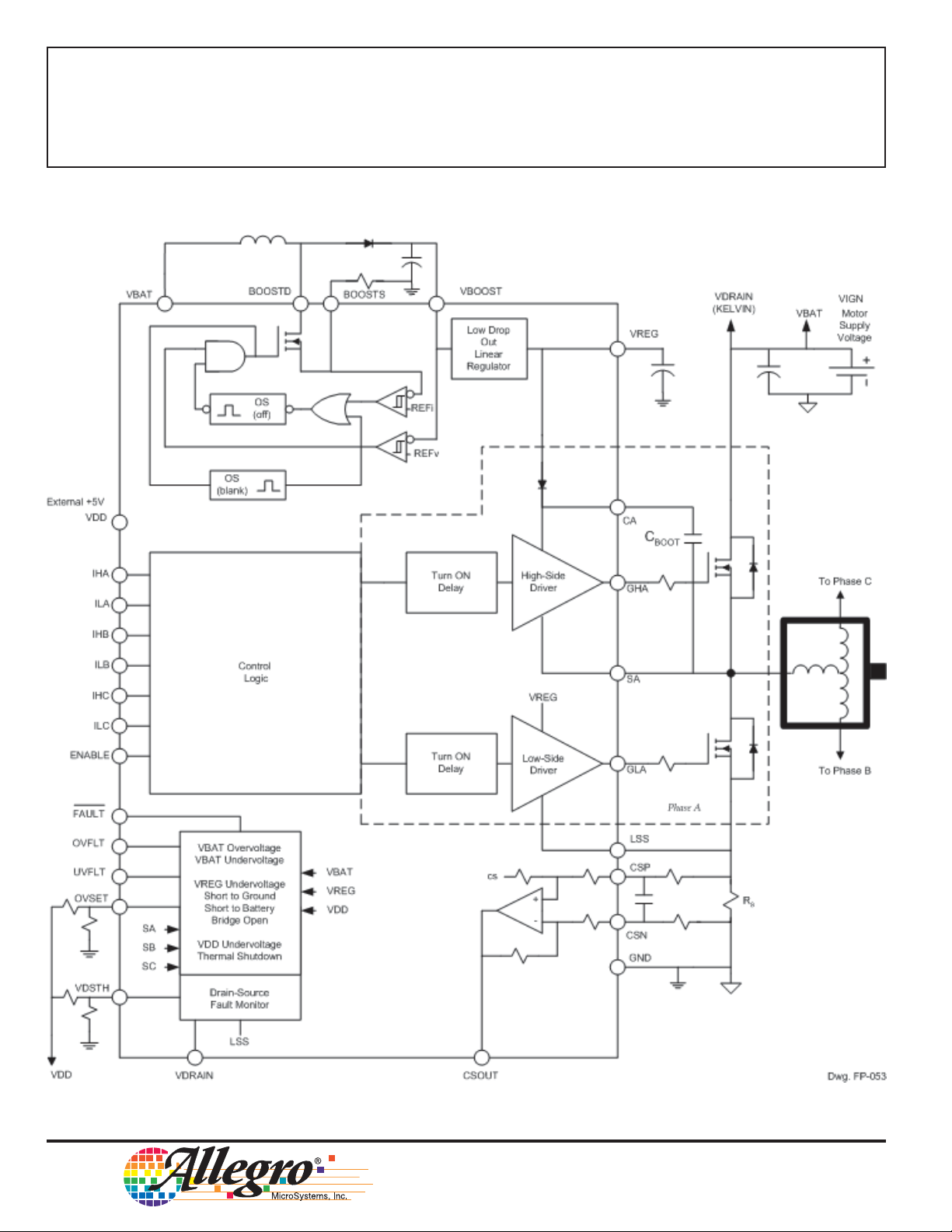
The A3935 is designed specifically for automotive applications that
require high-power motors. Each provides six high-current gate drive
outputs capable of driving a wide range of n-channel power MOSFETs.
A requirement of automotive systems is steady operation over a
varying battery input range. The A3935 integrates a pulse-frequency
modulated boost converter to create a constant supply voltage for
driving the external MOSFETs. Bootstrap capacitors are utilized to
provide the above battery supply voltage required for n-channel FETs.
Direct control of each gate output is possible via six TTL-compatible inputs. A differential amplifier is integrated to allow accurate
measurement of the current in the three-phase bridge.
Diagnostic outputs can be continuously monitored to protect the
driver from short-to-battery, short-to-supply, bridge-open, and battery
under/overvoltage conditions. Additional protection features include
dead-time, VDD undervoltage, and thermal shutdown.
Data Sheet
ABSOLUTE MAXIMUM RATINGS
Load Supply Voltages, VBAT, VDRAIN,
VBOOST, BOOSTD ... -0.6 V to 40 V
Output Voltage Ranges,
GHA/GHB/GHC, V
SA/SB/SC, VSX............... -4 V to 40 V
GLA/GLB/GLC, V
CA/CB/CC, VCX.......... -0.6 V to 55 V
Sense Circuit Voltages,
CSP,CSN, LSS............... -4 V to 6.5 V
Logic Supply Voltage,
VDD........................... -0.3 V to +6.5 V
Logic Input/Outputs and OVSET, BOOSTS,
CSOUT, VDSTH ......... -0.3 V to 6.5 V
Operating Temperature Range,
TA........................... -40°C to +135°C
Junction Temperature, TJ........... +150°C
Storage Temperature Range,
TS........................... -55°C to +150°C
* Fault conditions that produce excessive
junction temperature will activate device
thermal shutdown circuitry. These conditions
can be tolerated, but should be avoided.
.. -4 V to 55 V
GHX
.... -4 V to 16 V
GLX
The A3935 is supplied in a choice of three packages, a 44-lead
PLCC with copper batwing tabs (suffix ED), a 48-lead low profile QFP
with exposed thermal pad (suffix JP), and a 36-lead 0.8 mm pitch SOIC
(suffix LQ).
FEATURES
!!
! Drives wide range of n-channel MOSFETs in 3-phase bridges
!!
!!
! PFM boost converter for use with low-voltage battery supplies
!!
!!
! Internal LDO regulator for gate-driver supply
!!
!!
! Bootstrap circuits for high-side gate drivers
!!
!!
! Current monitor output
!!
!!
! Adjustable battery overvoltage detection.
!!
!!
! Diagnostic outputs
!!
! Motor lead short-to-battery, short-to-ground, and
bridge-open protection
! Undervoltage protection
!!
! -40 °C to +150 °C, T
!!
!!
! Thermal shutdown
!!
Always order by complete part number, e.g., A3935KLQ .
operation
J
3935
THREE-PHASE POWER
MOSFET CONTROLLER
Functional Block Diagram
See pages 8 and 9 for terminal assignments and descriptions.
2
115 Northeast Cutoff, Box 15036
Worcester, Massachusetts 01615-0036 (508) 853-5000
Copyright © 2003 Allegro MicroSystems, Inc.
3935
THREE-PHASE POWER
MOSFET CONTROLLER
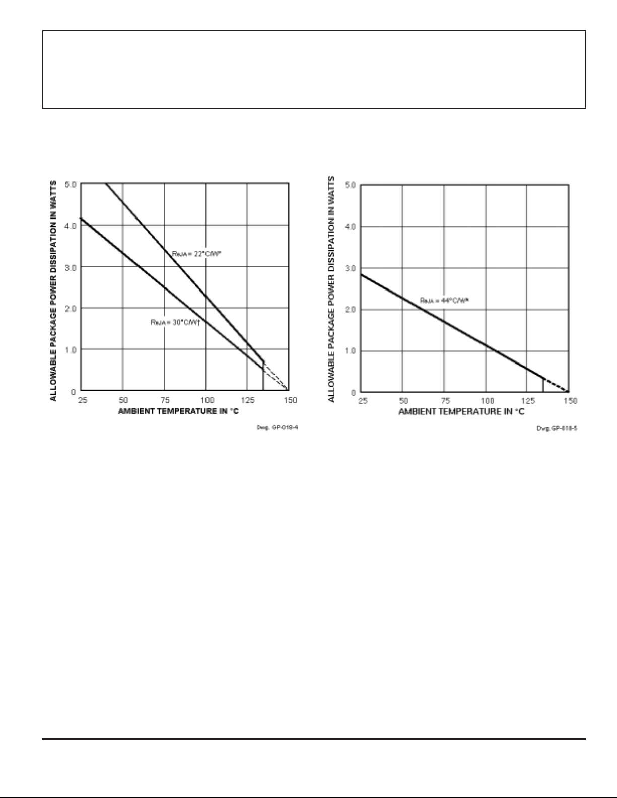
A3935KLQ (SOIC)A3935KED (PLCC)
* Measured on “High-K” multi-layer PWB per JEDEC Standard JESD51-7.
† Measured on typical two-sided PWB with power tabs (terminals 1, 2, 11, 12, 22, 23, 34, and 35) connected to copper foil with an
area of 3.8 square inches (2452 mm2) on each side. See Application Note 29501.5, Improving Batwing Power Dissipation, for
additional information.
www.allegromicro.com
3
3935
THREE-PHASE POWER
MOSFET CONTROLLER
ELECTRICAL CHARACTERISTICS: unless otherwise noted at T
V
= 4.75 V to 5.25 V, ENABLE = 22.5 kHz, 50% Duty Cycle, Two Phases Active.
DD
= -40°C to +150°C, V
J
= 7 V to 16 V,
BAT
Limits
Characteristics Symbol Conditions Min Typ Max Units
Power Supply
VDD Supply Current I
V
Supply Current I
BAT
Battery Voltage Operating Range V
Bootstrap Diode Forward Voltage V
Bootstrap Diode Resistance r
Bootstrap Diode Current Limit I
Bootstrap Quiescent Current I
Bootstrap Refresh Time t
DD
BAT
BAT
DBOOTIDBOOT
DBOOT
DM
CX
refresh
All logic inputs = 0 V – – 7.0 mA
All logic inputs = 0 V – – 3.0 mA
7.0 – 40 V
= -Icx = 10 mA, V
I
= -Icx = 100 mA 1.5 – 2.3 V
DBOOT
DBOOT
= V
REG
– V
CX
0.8 – 2.0 V
rD(100 mA) = [VD(150 mA) – VD(50 mA)]/100 mA 2.5 – 7.5 Ω
3 V < [V
– VCX] < 12 V -150 – -1150 mA
REG
VCX = 40 V, GHx = ON 10 – 30 µA
VSX = low to guarantee ∆V = +0.5 V refresh of – – 2.0 µs
0.47 µF Boot Cap at Vcx – Vsx = +10 V
VREG Output Voltage
VREG Dropout Voltage
Gate Drive Avg. Supply Current I
VREG Input Bias Current I
1
2
V
REG
V
REGDO
REG
REGBIAS
V
= 7 V to 40 V, V
BAT
V
= V
REGDO
boost
– V
reg
from Boost Reg 12.7 – 1 4 V
BOOST
, I
= 40 mA – 0.9 – V
reg
No external dc load at VREG, C
Current into V
, ENABLE = 0 – – 4.0 mA
BOOST
= 10 µF – – 40 mA
REG
Boost Supply
V
Output Voltage Limit V
BOOST
V
Output Volt. Limit Hyst. ∆V
BOOST
Boost Switch ON Resistance r
Max. Boost Switch Current I
BOOSTSW
Boost Current Limit Threshold Volt.
OFF Time t
Blanking Time t
BOOSTM
BOOSTM
DS(on)
V
BI(th)
off
blank
V
= 7 V 14.9 – 16.3 V
BAT
I
< 300 mA – 1.4 3.3 Ω
BOOSTD
Increasing V
BOOSTS
NOTES: Typical Data and Typical Characteristics are for design information only.
Negative current is defined as coming out of (sourcing) the specified device terminal.
1. For V
2. With V
< V
BOOSTM
decreasing Dropout Voltage measured at V
BOOST
4
< 40 V power dissipation in the V
BOOST
115 Northeast Cutoff, Box 15036
Worcester, Massachusetts 01615-0036 (508) 853-5000
LDO increases. Observe TJ < 150 °C limit.
REG
= V
REG
REGref
– 200 mV where V
35 – 180 mV
– – 300 mA
0.45 – 0.55 V
3.0 – 8.0 µs
100 – 220 ns
= V
REG(ref)
REG
at V
= 16 V.
BOOST
Continued next page …
3935
THREE-PHASE POWER
MOSFET CONTROLLER
ELECTRICAL CHARACTERISTICS: unless otherwise noted at T
VDD = 4.75 V to 5.25 V, ENABLE = 22.5 kHz, 50% Duty Cycle, Two Phases Active.
= -40°C to +150°C, V
J
Characteristics Symbol Conditions
Control Logic
Logic Input Voltages V
Logic Input Currents I
Input Hysteresis V
Logic Output High Voltage V
Logic Output Low Voltage V
I(1)
V
I(0)
I(1)
I
I(0)
hys
O(H)
I(L)
Minimum high level input for logical “one” 2.0 – – V
Maximum low level input for logical “zero” – – 0.8 V
VI = V
DD
VI = 0.8 V 50 – – µA
I
= -800 µA V
O(H)
I
= 1.6 mA – – 0.4 V
O(L)
Gate Drives, GHx ( internal SOURCE or upper switch stages)
Output High Voltage V
Source Current (pulsed) I
Source ON Resistance r
DSL(H)
xU
SDU(on)
GHx: I
GLx: I
V
V
I
xU
I
xU
= –10 mA, Vsx = 0 V
xU
= –10 mA, V
xU
= 10 V, TJ = 25 °C – 800 – mA
SDU
= 10 V, TJ = 135 °C 400 – – mA
SDU
= 0 V
lss
= –150 mA, TJ = 25 °C 4.0 – 10 Ω
= –150 mA, TJ = 35 °C 7.0 – 15 Ω
Gate Drives, GLx ( internal SINK or lower switch stages)
V
Sink Current (pulsed) I
Sink ON Resistance r
xL
DSL(on)
= 10 V, TJ = 25 °C – 850 – mA
DSL
= 10 V, TJ = 135 °C 550 – – mA
V
DSL
I
= +150 mA, TJ = 25 °C 1.8 – 6.0 Ω
xL
= +150 mA, TJ = 135 °C 3.0 – 7.5 Ω
I
xL
Gate Drives, GHx, GLx (General)
Phase Leakage (Source) I
Propagation Delay, Logic only t
Output Skew Time t
Dead Time (Shoot-Through
t
Sx
pd
sk(o)
dead
ENABLE = 0, VSx = 1.7 V 0 – 100 µA
Logic input to unloaded GHx, GLx – – 150 ns
Grouped by edge, phase-to-phase – – 50 ns
Between GHx, GLx transitions of same phase 75 – 180 ns
Prevention)
= 7 V to 16 V,
BAT
Limits
Min Typ Max Units
– – 500 µA
100 – 300 mV
– 0.8 – – V
DD
– 2.26 – V
REG
– 0.26 – V
REG
REG
REG
V
V
NOTES: Typical Data and Typical Characteristics are for design information only.
Negative current is defi ned as coming out of (sourcing) the specifi ed device terminal.
For GH
For GL
X
: V
X
= VCX – V
SDU
= V
SDU
REG
– V
GHX
GLX
, V
, V
DSL
DSL
= V
= V
– VSX, V
GHX
– V
GLX
LSS
, V
DSL(H)
DSL(H)
= VCX – V
= V
REG
– V
– VSX.
SDU
SDU
– V
LSS.
: V
www.allegromicro.com
5

3935
THREE-PHASE POWER
MOSFET CONTROLLER
ELECTRICAL CHARACTERISTICS: unless otherwise noted at T
V
= 4.75 V to 5.25 V, ENABLE = 22.5 kHz, 50% Duty Cycle, Two Phases Active.
DD
= -40°C to +150°C, V
J
= 7 V to 16 V,
BAT
Limits
Characteristics Symbol Conditions Min Typ Max Units
Sense Amplifier
Input Bias Current I
Input Offset Current I
Input Resistance r
bias
IO
CSP = CSN = 0 V -180 – -360 µA
CSP = CSN = 0 V – – ±35 µA
CSP with respect to GND – 80 – kΩ
i
CSN with respect to GND – 4.0 – kΩ
Diff. Input Operating Voltage V
Output Offset Voltage V
Output Offset Voltage Drift ∆V
Input Com-Mode Oper. Range V
Voltage Gain A
Low Output Voltage Error E
DC Common-Mode Attenuation A
Output Resistance r
Output Dynamic Range V
CSOUT
Output Current, Sink I
Output Current, Source I
source
OO
VC
sink
VID = CSP – CSN, -1.3V < CSP,N < 4V – – ±200 mV
ID
CSP = CSN = 0 V 77 250 450 mV
CSP = CSN = 0 V – 100 – µV/°C
OO
CSP = CSN -1.5 – 4.0 V
IC
VID = 40 mV to 200 mV 18.6 19.2 19.8 V/V
V
Vid = 0 to 40 mV, Vo = (19.2 x VID) + Vo + E
v
v
– – ±25 mV
CSP = CSN = 200 mV 28 – – dB
V
o
= 2.0 V – 8.0 – Ω
CSOUT
I
= -100 µA at top rail, 100 µA at bottom rail 0.075 – VDD-0.25 V
CSOUT
V
= 2.5 V 20 – – mA
CSOUT
V
= 2.5 V -1.0 – – mA
CSOUT
VDD Supply Ripple Rejection PSRR CSP = CSN = GND, freq. = 0 to 1 MHz 20 – – dB
VREG Supply Ripple Rejection PSRR CSP = CSN = GND, freq. = 0 to 300 kHz 45 – – dB
Small Signal 3-dB Bandwidth f
AC Common-Mode Attenuation A
3db
10 mV input – 1.6 – MHz
Vcm = 250 mV/pp, freq. = 0 to 800 kHz 26 – – dB
vc
Output Slew Rate SR 200 mV step input, meas. 10/90% points 10 – – V/µs
(positive or negative)
NOTES: Typical Data and Typical Characteristics are for design information only.
Negative current is defined as coming out of (sourcing) the specified device terminal.
6
115 Northeast Cutoff, Box 15036
Worcester, Massachusetts 01615-0036 (508) 853-5000

3935
THREE-PHASE POWER
MOSFET CONTROLLER
ELECTRICAL CHARACTERISTICS: unless otherwise noted at T
V
= 4.75 V to 5.25 V, ENABLE = 22.5 kHz, 50% Duty Cycle, Two Phases Active.
DD
= -40°C to +150°C, V
J
= 7 V to 16 V,
BAT
Limits
Characteristics Symbol Conditions Min Typ Max Units
Fault Logic
VDD Undervoltage V
DD(uv)
VDD Undervoltage Hysteresis ∆V
OVSET Operating Volt. Range V
OVSET Calibrated Volt. Range V
OVSET Input Current Range I
VBAT Overvoltage Range V
VBAT Overvoltage V
VBAT Overvoltage Hysteresis ∆V
VBAT Overvoltage Gain Constant
VBAT Undervoltage V
VBAT Undervoltage Hysteresis ∆V
VREG Undervoltage V
VDSTH Input Range V
VDSTH Input Current I
Short-to-Ground Threshold V
Short-to-Battery Threshold V
V
/Open Bridge Oper. Range V
DRAIN
V
/Open Bridge Current I
DRAIN
V
/Open Bridge Threshold Volt.
DRAIN
SET(ov)
SET(ov)
SET(ov)
BAT(ov)
BAT(ov)
K
BAT(ov)
BAT(uv)
REG(uv)
DSTH
STG(th)
STB(th)
DRAIN
VDRAIN
V
BDGO(th)
BAT(ov)
BAT(uv)
DSTH
Thermal Shutdown Temp. T
Thermal Shutdown Hysteresis ∆T
DD(uv)
Decreasing V
V
DD(recovery)
0 V < V
Increasing V
Percent of V
V
BAT(ov)
Decreasing V
Percent of V
Decreasing V
V
> 0.8 V 40 – 100 µA
DSTH
DD
- V
DD(uv)
< 2.5 V 19.4 – 4 0 V
SET(ov)
= (K
BAT
BAT(ov)
BAT(ov)
BAT
BAT(uv)
REG
, V
= 0 V 19.4 22.4 25.4 V
SET(ov)
value set by V
x V
SET(ov)
) + V
SET(ov)
[0] – 12 – V/V
BAT(ov)
With a high-side driver “on”, as VSX decreases, V
V
DRAIN
- VSX > V
causes a fault
STG
With a low-side driver “on”, as VSX increases, V
VSX - V
7 V < V
7 V < V
If V
J
J
> V
causes a fault
STB
< 40 V -0.3 – V
< 40 V 0 – 1.0 mA
then a bridge fault occurs 1.0 – 3.0 V
BDGOTH
DRAIN
LSS
BAT
BAT
< V
3.8 – 4.3 V
100 – 300 mV
0–VDDV
0 – 2.5 V
-1.0 – +1.0 µA
9.0 – 15 %
5.0 5.25 5.5 V
8.0 – 12 %
9.9 – 11.1 V
0.5 – 3.0 V
-0.3 – V
DSTH
-0.3 – V
DSTH
+0.2 V
DSTH
+0.2 V
DSTH
+2.0 V
BAT
160 170 180 °C
7.0 10 13 °C
NOTES: Typical Data and Typical Characteristics are for design information only.
Negative current is defined as coming out of (sourcing) the specified device terminal.
www.allegromicro.com
7

3935
THREE-PHASE POWER
MOSFET CONTROLLER
Terminal Functions
A3935KED A3935KJP A3935KLQ
Terminal Name Function (PLCC) (QLFP) (SOIC)
CSP Current-sense input, positive-side 31 19 1
VDSTH DC input, drain-to-source monitor threshold voltage 32 20 2
LSS Gate-drive source return, low-side 33 2 1 3
GLC Gate-drive C output, low-side 36 22 4
SC Load phase C input 37 26 5
GHC Gate-drive C output, high-side 38 27 6
CC Bootstrap capacitor C 39 28 7
GLB Gate-drive B output, low-side 4 0 29 8
SB Load phase B input 41 30 9
GHB Gate-drive B output, high-side 42 3 1 10
CB Bootstrap capacitor B 4 3 3 2 1 1
GLA Gate-drive A output, low-side 4 4 33 1 2
SA Load phase A input 3 34 13
GHA Gate-drive A output, high-side 4 38 14
CA Bootstrap capacitor A 5 39 15
VREG Gate drive supply, positive 6 40 16
VDRAIN Kelvin connection to MOSFET high-side drains 7 41 17
VBOOST Boost supply output 8 42 18
BOOSTS Boost switch, source 9 43 19
BOOSTD Boost switch, drain 10 44 20
VBAT Battery supply, positive 13 46 22
UVFLT VBAT undervoltage fault output 14 3 23
OVFLT VBAT overvoltage fault output 15 4 24
FAULT Active-low fault output, primary 16 5 25
ALO Gate control input A, low-side 17 6 26
AHI Gate control input A, high-side 18 7 27
BHI Gate control input B, high-side 19 8 28
BLO Gate control input B, low-side 20 9 29
CLO Gate control input C, low-side 21 10 30
CHI Gate control input C, high-side 24 11 3 1
ENABLE Gate output enable 25 12 3 2
OVSET DC input, overvoltage threshold setting for VBAT 26 1 5 33
NC Not connected, no external connection allowed 27 1,2,13,14,23,24, –
25,35,36,37,47,48
CSOUT Current-sense amplifier output 2 8 16 34
VDD Logic supply, nominally +5 V 29 17 35
CSN Current-sense input, negative-side 30 18 36
GND Ground, dc supply returns, negative, and (for ED package) 1, 2, 11, 12, 45 21
heat sink tab
22, 23, 34, 35
8
115 Northeast Cutoff, Box 15036
Worcester, Massachusetts 01615-0036 (508) 853-5000

Terminal Descriptions
3935
THREE-PHASE POWER
MOSFET CONTROLLER
AHI/BHI/CHI. Direct control of high-side gate outputs GHA/
GHB/GHC. Logic “1” drives the gate “on”. Logic ”0” pulls the
gate down, turning off the external power MOSFET. Internally
pulled down when terminal is open.
ALO/BLO/CLO. Direct control of low-side gate outputs GLA/
GLB/GLC. Logic “1” drives the gate “on”. Logic ”0” pulls the
gate down, turning off the external power MOSFET. Internally
pulled down when terminal is open.
BOOSTD. Boost converter switch drain connection.
BOOSTS. Boost converter switch source connection.
CA/CB/CC. High-side connection for bootstrap capacitor,
positive supply for high-side gate drive. The bootstrap capacitor
is charged to VREG when the output Sx terminal is low. When
the output swings high, the voltage on this terminal rises with
the output to provide the boosted gate voltage needed for nchannel power MOSFETs.
CSN. Input for current-sense, differential amplifier, inverting,
negative side. Kelvin connection for ground side of currentsense resistor.
CSOUT. Amplifier output voltage proportional to current
sensed across an external low-value resistor placed in the
ground-side of the power FET bridge.
CSP. Input for current-sense differential amplifier, non-
inverting, positive side. Connected to positive side of sense
resistor.
ENABLE. Logic “0” disables the gate control signals and
switches off all the gate drivers “low” causing a “coast”. Can be
used in conjunction with the gate inputs to PWM the load
current. Internally pulled down when terminal is open.
GND. Ground or negative side of VDD and VBAT supplies.
LSS. Low-side gate driver returns. Connects to the common
sources in the low-side of the power MOSFET bridge.
OVFLT. Logic “1” means that the VBAT exceeded the VBAT
overvoltage trip point set by OVSET level. It will recover after
a hysteresis below that maximum value. Normally has a highimpedance state.
OVSET. A positive, dc level that controls the VBAT overvoltage trip point. Usually, provided from precision resistor divider
network between V
preset value. When terminal is open, sets unspecified but high
overvoltage trip point.
SA/SB/SC. Directly connected to the motor terminals, these
terminals sense the voltages switched across the load and are
connected to the negative side of the bootstrap capacitors. Also,
are the negative supply connection for the floating, high-side
drivers.
UVFLT. Logic “1” means that VBAT is below its minimum
value and will recover after a hysteresis above that minimum
value. Has a high-impedance state. [If UVFLT and OVFLT are
both in high-impedance state; then, at least, a thermal shutdown
or VDD undervoltage has occurred.]
VBAT. Battery voltage, positive input and is usually connected
to the motor voltage supply.
VBOOST. Boost converter output, nominally 16 V, is also
input to regulator for VREG. Has internal boost current and
boost voltage control loops. In high-voltage systems is approximately one diode drop below V
VDD. Logic supply, nominally +5 V.
and GND, but can be held grounded for a
DD
.
BAT
FAULT. Diagnostic logic output signal, when “low” indicates
that one or more fault condition have occurred.
GHA/GHB/GHC. High-side gate-drive outputs for n-channel
MOSFET drivers. External series gate resistors can control slew
rate seen at the power driver gate; thereby, controlling the di/dt
and dv/dt of Sx outputs.
GLA/GLB/GLC. Low-side gate drive outputs for external, nchannel MOSFET drivers. External series gate resistors can
control slew rate.
www.allegromicro.com
VDRAIN. Kelvin connection for drain-to-source voltage
monitor and is connected to high-side drains of MOSFET
bridge. High impedance when terminal is open and registers as
a short-to-ground fault on all motor phases.
VDSTH. A positive, dc level that sets the drain-to-source
monitor threshold voltage. Internally pulled down when
terminal is open.
VREG. High-side, gate-driver supply, nominally, 13.5 V. Has
low-voltage dropout (LDO) feature.
9

3935
THREE-PHASE POWER
MOSFET CONTROLLER
Functional Description
Motor Lead Protection. A fault detection circuit monitors
the voltage across the drain to source of the external MOSFETs.
A fault is asserted “low” on the output terminal, FAULT, if the
drain-to-source voltage of any MOSFET that is instructed to turn
on is greater than the voltage applied to the V
When a high-side switch is turned on, the voltage from V
input terminal.
DSTH
DRAIN
to
the appropriate motor phase output, VSX, is examined. If the
motor lead is shorted to ground before the high side is turned on,
the measured voltage will exceed the threshold and the FAULT
terminal will go “low”. Similarly, when a low-side MOSFET is
turned on, the differential voltage between the motor phase
(drain) and the LSS terminal (source) is monitored. V
DSTH
is set
by a resistor divider to VDD.
The V
is intended to be a Kelvin connection for the high-
DRAIN
side, drain-source monitor circuit. Voltage drops across the
power bus are eliminated by connecting an isolated PCB trace
from the V
This allows improved accuracy in setting the V
terminal to the drain of the MOSFET bridge.
DRAIN
DSTH
threshold
voltage. The low-side, drain-source monitor uses the LSS
terminal, rather than V
, in comparing against V
DRAIN
DSTH
.
The A3935 merely reports these motor faults.
Fault Outputs. Transient faults on any of the fault outputs are
to be expected during switching and will not disable the gate
drive outputs. External circuitry or controller logic must
determine if the faults represent a hazardous condition.
FAULT. This terminal will go active “low” when any of the
following conditions occur:
V
overvoltage,
BAT
V
undervoltage,
BAT
V
undervoltage,
REG
Motor lead short-to-ground,
Motor lead short-to-supply (or battery),
Bridge (or V
DRAIN
) open,
VDD undervoltage, or
Thermal shutdown.
OVFLT. Asserts “high” when a V
overvoltage fault occurs
BAT
and resets “low” after a recovery hysteresis. It has a highimpedance state when a thermal shutdown or VDD undervoltage
occurs. The voltage at the OVSET terminal, V
the V
where K
V
overvoltage set point V
BAT
BAT(ov)
V
BAT(ov)
when V
= (K
BAT(ov)
is the gain (12) and V
SET(ov)
, i.e.,
BAT(ov)
BAT(ov)
x V
SET(ov)
) + V
BAT(ov)
(0) is the value of
BAT(ov)
is zero (~22.4). For valid formula, all
OVSET
(0),
, controls
variables must be in range and below maximum operating
specification.
UVFLT. Asserts “high” when a V
undervoltage fault occurs
BAT
and resets “low” after a recovery hysteresis. It has a highimpedance state when a thermal shutdown or VDD undervoltage
occurs. OVFLT and UVFLT are mutually exclusive by definition.
Current Sensing. A current-sense amplifier is provided to
allow system monitoring of the load current. The differential
amplifier inputs are intended to be Kelvin connected across a
low-value sense resistor or current shunt. The output voltage is
represented by:
V
CSOUT
= ( I
x AV x RS) + V
LOAD
OS
where VOS is the output voltage calibrated at zero load current
and AV is the differential amplifier gain of about 19.2. If either
the CSP or CSN pin is open, the CSOUT pin will go to its
maximum positive level.
Shutdown. If a fault occurs because of excessive junction
temperature or undervoltage on VDD or V
, all gate driver
BAT
outputs are driven “low” until the fault condition is removed. In
addition, the boost supply switch and the VREG are turned “off”
until those undervoltages and junction temperatures recover.
Boost Supply. V
is controlled by an inner current-
BOOST
control loop, and by an outer voltage-feedback loop. The
current-control loop turns “off” the boost switch for 5 µs
whenever the voltage across the boost current-sense resistor
exceeds 500 mV. A diode reverse-recovery current flows
through the sense resistor whenever the boost switch turns “on”,
which could turn it “off” again if not for the “blanking time”
circuit. Adjustment of this external sense resistor determines the
maximum current in the inductor. Whenever V
BOOST
exceeds the
predefined threshold, nominally 16 V, the boost switch is
inhibited.
10
115 Northeast Cutoff, Box 15036
Worcester, Massachusetts 01615-0036 (508) 853-5000

THREE-PHASE POWER
MOSFET CONTROLLER
Functional Description (cont’d)
Input Logic
ENABLE xLO xHI GLx GHx Mode of Operation
0 X X 0 0 All gate drive outputs low
1 0000Both gate drive outputs low
1 0101High side on
1 1010Low side on
1 1100XOR circuitry prevents shoot-through
Fault Responses
3935
ENABLE Boost V
REG
Fault Mode Input FAULT OVFLT UVFLT Reg. Reg. GHx GLx
No Fault X 1 0 0 ON ON ""
Short-to-Battery 1# 0 0 0 ON ON ""
Short-to-Ground 1$ 0 0 0 ON ON ""
Bridge (V
Undervoltage X 0 0 0 ON ON ""
V
REG
Overvoltage X 0 1 0 OFF& ON ""
V
BAT
Undervoltage' X 0 0 1 OFF OFF 0 0
V
BAT
Undervoltage' X 0 Z Z OFF OFF 0 0
V
DD
) Fault 1% 0 0 0 ON ON ""
DRAIN
Thermal Shutdown' X 0 Z Z OFF OFF 0 0
NOTES: x = “Little x ”indicates A, B, or C phase.
X = “Capital X “ indicates a “don’t care”.
Z = High-impedance state.
" = Depends on xLO input, xHI input, and ENABLE. See Input Logic table.
# = Short-to-battery can only be detected when the corresponding GLx
= 1. This fault is not detected when ENABLE = 0.
$ = Short-to-ground can only be detected when the corresponding GHx = 1. This fault is not detected when ENABLE = 0.
% = Bridge fault appears as a short-to-ground fault on all motor phases. This fault is not detected when ENABLE = 0.
& = Off, only because V
BOOST
≈ V
is above the voltage threshold of the regulator’s voltage control loop.
BAT
' = These faults are not only reported but action is taken by the internal logic to protect the A3935 and the system.
www.allegromicro.com
11

3935
THREE-PHASE POWER
MOSFET CONTROLLER
VDRAIN
VBOOST
BOOSTS
BOOSTD
GND
GND
VBAT
UVFLT
OVFLT
FAULT
ALO
Package ED, 44-Pin PLCC
16
GHASAGND
VREG
CA
4
6
5
7
8
9
10
11
12
13
14
15
17
20
19
18
AHI
BHI
BLO
3
21
CLO
2
22
GND
GND
GLACBGHB
1
444342
24
23
CHI
GND
25
ENABLE
SB
41
26
27
NC
OVSET
GLB
40
39
CC
38
GHC
37
SC
36
GLC
35
GND
GND
34
LSS
33
VDSTH
32
CSP
31
CSN
30
VDD
29
28
CSOUT
Package LQ, 36-Pin SOIC
NC
GHA
CA
VREG
VDRAIN
VBOOST
BOOSTS
BOOSTD
GND
VBAT
NC
NC
Package JP, 48-Pin LQFP
GLACBGHBSBGLBCCGHC
NC36NC
SA
30
32
33
37
46
47
35
34
38
39
40
41
42
43
44
45
48
3
2
1
NC
NC
UVFLT
31
292827
4
5
FAULT
OVFLT
6
ALO
7
AHI
8
BHI
9
BLO
10
CLO
SC
26
11
CHI
NC
25
24
23
22
21
20
19
18
17
16
15
14
13
12
ENABLE
NC
NC
GLC
LSS
VDSTH
CSP
CSN
VDD
CSOUT
OVSET
NC
NC
12
CSP
VDSTH
LSS
GLC
GHC
CC
GLB
SB
GHB
GLA
GHA
VREG
VDRAIN
VBOOST
SC
CB
SA
CA
1
2
3
4
5
6
7
8
9
10
11
12
13
14
15
16
17
18
36
35
34
33
32
31
30
29
28
27
26
25
24
23
22
21
20
19
CSN
VDD
CSOUT1
OVSET
ENABLE
CHI
CLO
BLO
BHI
AHI
ALO
FAULT
OVFLT
UVFLT
VBAT
GND
BOOSTD
BOOSTS
115 Northeast Cutoff, Box 15036
Worcester, Massachusetts 01615-0036 (508) 853-5000

A3935KED (PLCC)
3935
THREE-PHASE POWER
MOSFET CONTROLLER
Dimensions in Inches
(for reference only)
NOTES: 1. Exact body and lead configuration at vendor’s option within limits shown.
2. Lead spacing tolerance is non-cumulative.
3. Webbed lead frame. Terminals 1, 2, 11, 12, 22, 23, 34, and 35 are internally one piece.
4. Supplied in standard sticks/tubes of 27 devices or add “TR” to part number for tape and reel.
www.allegromicro.com
Dimensions in Millimeters
(controlling dimensions)
13

3935
THREE-PHASE POWER
MOSFET CONTROLLER
9
0.354
BSC
7
0.276
BSC
48
A3935KJP (LQFP)
5
A
0.197
BSC
7º
0º
1
REF
.20
.09
0.039
0.008
0.004
21
.27
0.011
.17
0.007
Dimensions in millimeters
U.S. Customary dimensions (in.) in brackets, for reference only
A
Exposed thermal pad (bottom surface)
.50
BSC
.020
.75
0.030
.45
0.018
1.60
1.40
.15
0.006
.05
0.002
0.063
0.055
.25
0.010
BSC
Seating Plane
Gauge Plane
14
115 Northeast Cutoff, Box 15036
Worcester, Massachusetts 01615-0036 (508) 853-5000

A3935KLQ (SOIC)
3935
THREE-PHASE POWER
MOSFET CONTROLLER
Dimensions in Inches
(for reference only)
NOTES: 1. Lead spacing tolerance is non-cumulative.
2. Exact body and lead configuration at vendor’s option within limits shown.
3. Supplied in standard sticks/tubes of 31 devices or add “TR” to part number for tape and reel.
www.allegromicro.com
Dimensions in Millimeters
(controlling dimensions)
15

3935
THREE-PHASE POWER
MOSFET CONTROLLER
The products described here are manufactured under one or more
U.S. patents or U.S. patents pending.
Allegro MicroSystems, Inc. reserves the right to make, from time to
time, such departures from the detail specifications as may be required
to permit improvements in the performance, reliability, or
manufacturability of its products. Before placing an order, the user is
cautioned to verify that the information being relied upon is current.
Allegro products are not authorized for use as critical components
in life-support devices or systems without express written approval.
The information included herein is believed to be accurate and
reliable. However, Allegro MicroSystems, Inc. assumes no responsibility for its use; nor for any infringement of patents or other rights of
third parties which may result from its use.
16
115 Northeast Cutoff, Box 15036
Worcester, Massachusetts 01615-0036 (508) 853-5000
 Loading...