

2580, 2585,
Data Sheet
29316C*
UDN2580A and UDN2585A
AND
2588
8-CHANNEL SOURCE DRIVERS
This versatile family of integrated circuits will work with many combinations of logic- and load-voltage levels, meeting interface requirements beyond
the capabilities of standard logic buffers. Series UDN2580A and A2580SLW
source drivers can drive incandescent, LED, or vacuum fluorescent displays.
Internal transient-suppression diodes permit the drivers to be used with
inductive loads such as relays, solenoids, dc and stepping motors, and magnetic print hammers.
The Types UDN2580A and A2580SLW are high-current source drivers
used to switch the ground ends of loads that are directly connected to a -50 V
supply. Typical loads are telephone relays, PIN diodes, and LEDs.
The UDN2585A and A2585SLW are drivers designed for applications
requiring low output saturation voltages. Typical loads are low-voltage LEDs
and incandescent displays. The eight non-Darlington, 25 V outputs will
simultaneously sustain continuous load currents of -120 mA at ambient
temperatures to +70°C.
ABSOLUTE MAXIMUM RATINGS
See next page.
The UDN2588A and A2588SLW have separate logic and driver supply
lines. Their eight drivers can serve as an interface between positive logic
(TTL, CMOS, PMOS) or negative logic (NMOS) and either negative or splitload supplies to -80 V.
These drivers are packaged in plastic DlPs (suffix A) or surface-mountable wide-body SOlCs (suffix LW), and are rated for operation over the
temperature range of -20°C to +85°C.
FEATURES
■ TTL, CMOS, PMOS, NMOS Compatible
■ High Output-Current Rating
■ Internal Transient Suppression
■ Efficient Input/Output Structure
■ Through-Hole and Surface-Mount Packages
Always order by complete part number, e.g., UDN2580A .
2580, 2585, AND 2588
8-CHANNEL
SOURCE DRIVERS
ABSOLUTE MAXIMUM RATINGS
at 25°C Free-Air Temperature for any one driver (unless otherwise noted).
UDN2580A UDN2585A UDN2588A
A2580SLW A2585SLW A2588SLW
Output Voltage, V
Supply Voltage, V
CE
(ref. sub.) 50 V 25 V 80 V
S
50 V 25 V 80 V
Supply Voltage, VCC (ref. sub.) — — 80 V
Input Voltage, V
Total Output Current, (l
Substrate Current I
Package Power Dissipation, P
(ref. VS) -30 V -20 V -30 V
IN
+ IS) -500 mA -250 mA -500 mA
C
SUB
(single output) . . . . . . . . . . . . . . . . . . . . . . . . . . . . . . . . . . . . . . . . . . . . . . . . . . . . . . . . . . . . . . . . . 1.0 W
D
3.0 A 2.0 A 3.0 A
(total package) . . . . . . . . . . . . . . . . . . . . . . . . . . . . . . . . . . . . . . . . . . . . . . . . . . . . . . . . . . . . See Graph
Operating Temperature Range, T
Storage Temperature Range, T
. . . . . . . . . . . . . . . . . . . . . . . . . . . . . . . . . . . . . . . . . . . . . . . . . . . . . . . . . . . . . . . . . . . -20°C to +85°C
A
. . . . . . . . . . . . . . . . . . . . . . . . . . . . . . . . . . . . . . . . . . . . . . . . . . . . . . . . . . . . . . . . . . . .-55°C to +150°C
S
2.5
2.0
1.5
20-PIN DIP, R = 55°C/W
18-PIN DIP, R = 60°C/W
20-LEAD SOIC, R = 70°C/W
θJA
θJA
θJA
1.0
0.5
ALLOWABLE PACKAGE POWER DISSIPATION IN WATTS
0
25
2
50 75 100 125 150
AMBIENT TEMPERATURE IN °C
Dwg. GP-022-1
115 Northeast Cutoff, Box 15036
Worcester, Massachusetts 01615-0036 (508) 853-5000
W
Copyright © 1981, 2000 Allegro MicroSystems, Inc.
For simplification, these devices are characterized on the following pages with
specific voltages for inputs, logic supply (VS), load supply (VEE), and collector
supply (VCC). Typical use of the UDN2580A and A2580SLW is with negativereferenced logic. The more common application of the UDN2585A, A2585SLW,
UDN2588A and A2588SLW are with positive-referenced logic supplies. In
application, the devices are capable of operation over a wide range of logic and
supply voltage levels:
TYPICAL OPERATING VOLTAGES
2580, 2585, AND 2588
8-CHANNEL
SOURCE DRIVERS
V
S
0 V -15 V to -3.6 V -0.5 V to 0 V NA -25 V UDN2585A & A2585SLW
+5 V 0 V to +1.4 V +4.5 V to +5 V NA -20 V UDN2585A & A2585SLW
+12 V 0 V to +8.4 V +11.5 V to +12 V NA -13 V UDN2585A & A2585SLW
+15 V 0 V to +11.4 V +14.5 V to +15 V NA -10V UDN2585A & A2585SLW
NOTE: The substrate must be tied to the most negative point in the external circuit to maintain isolation between drivers and to provide
for normal circuit operation.
V
lN(ON)
V
lN(OFF)
V
CC
≤ 5 V -75 V UDN2588A & A2588SLW
≤12 V -68 V UDN2588A & A2588SLW
≤15 V -65 V UDN2588A & A2588SLW
V
EE(MAX)
-50 V UDN2580A & A2580SLW
-45 V UDN2580A & A2580SLW
-38 V UDN2580A & A2580SLW
-35 V UDN2580A & A2580SLW
Device Types
www.allegromicro.com
3
2580, 2585, AND 2588
8-CHANNEL
SOURCE DRIVERS
UDN2580A and A2580SLW
ELECTRICAL CHARACTERISTICS at T
Characteristic Symbol Test Conditions Min. Max. Units
= +25°C, VS = 0 V, VEE = -45 V (unless otherwise noted).
A
Limits
Output Leakage I
CEX
VlN = -0.5 V, V
Current VlN = -0.4 V, V
Output Sustaining V
CE(SUS)
VlN = -0.4 V, I
Voltage
Output Saturation V
CE(SAT)
VlN = -2.4 V, I
Voltage VlN = -3.0 V, I
VlN = -3.6 V, I
Input Current I
IN(ON)
VlN = -3.6 V, I
VlN = -15 V, I
I
IN(OFF)
Input Voltage V
V
IN(OFF)
Clamp Diode I
IN(ON)
R
I
= -500 µA, TA = 70°C, Note 3 -50 — µA
OUT
I
= -100 mA, VCE ≤1.8 V, Note 4 — -2.4 V
OUT
I
= -225 mA, VCE ≤1.9 V, Note 4 — -3.0 V
OUT
I
= -350 mA, VCE ≤2.0 V, Note 4 — -3.6 V
OUT
I
= -500 µA, TA = 70°C-0.2— V
OUT
VR = 50 V, TA = 70°C — 50 µA
Leakage Current
Clamp Diode V
F
IF = 350 mA — 2.0 V
Forward Voltage
Input Capacitance C
Turn-On Delay t
Turn-Off Delay t
IN
PHL
PLH
0.5 EIN to 0.5 E
0.5 EIN to 0.5 E
= VEE = -50 V — 50 µA
OUT
= VEE = -50 V, TA = 70°C — 100 µA
OUT
= -25 mA, Note 1 35 — V
OUT
= -100 mA — 1.8 V
OUT
= -225 mA — 1.9 V
OUT
= -350 mA — 2.0 V
OUT
= -350 mA — -500 µA
OUT
= -350 mA — -2.1 mA
OUT
— 25 pF
OUT
OUT
— 5.0 µs
— 5.0 µs
≤ 300 µs,
p
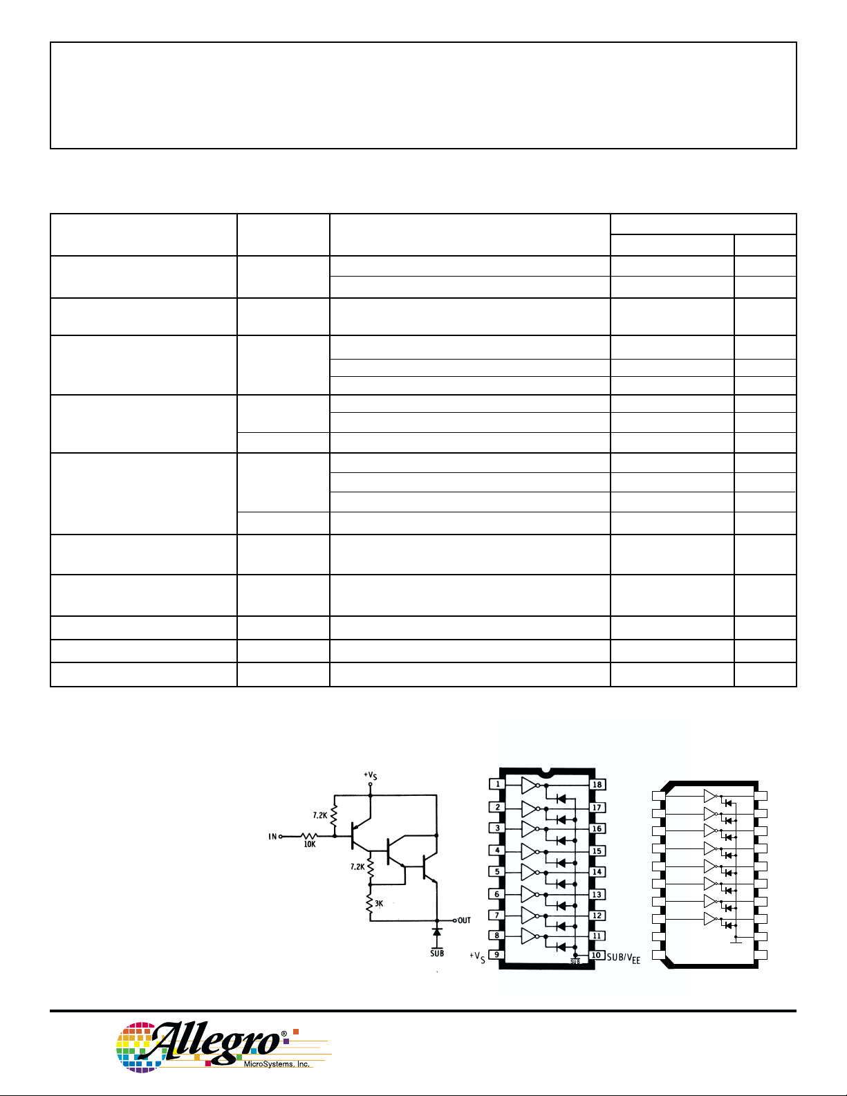
PARTIAL SCHEMATICNOTES: 1. Pulsed test, t
UDN2580A A2580SLW
duty cycle ≤ 2%.
2. Negative current is
defined as coming out of the
specified device pin.
3. The I
IN(OFF)
current limit
guarantees against partial
turn-on of the output.
4. The V
voltage limit
IN(ON)
guarantees a minimum
output source current per the
specified conditions.
5. The substrate must
always be tied to the most
negative point and must be at
least 4.0 V below V
4
.
S
115 Northeast Cutoff, Box 15036
Worcester, Massachusetts 01615-0036 (508) 853-5000
Dwg. No. A-11,358
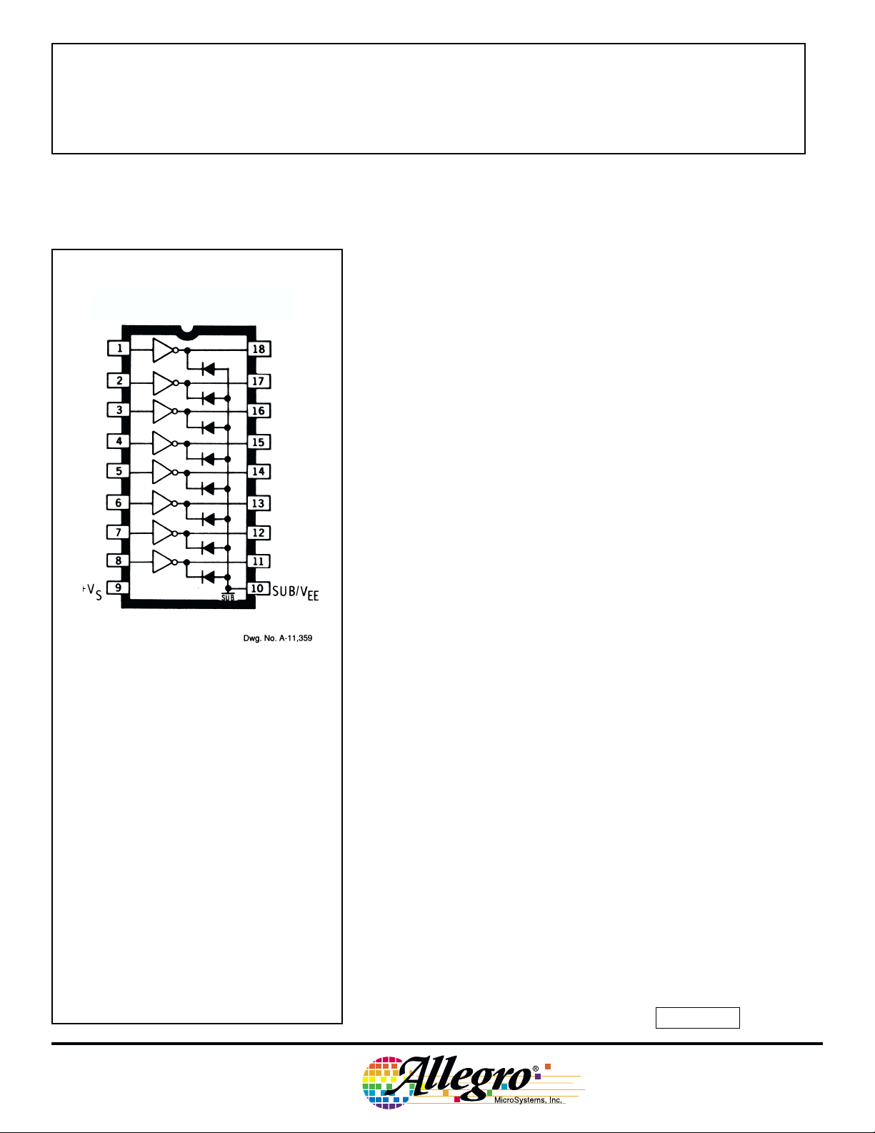
Dwg. No. A-11,359
1
2
3
4
5
6
7
8
9
+V
S
10NCNC
SUB
Dwg. PP-064
20
19
18
17
16
15
14
13
SUB/V
12
EE
11

2580, 2585, AND 2588
8-CHANNEL
SOURCE DRIVERS
UDN2585A and A2585SLW
ELECTRICAL CHARACTERISTICS at TA = +25°C, VS = 0 V, VEE = -20 V (unless otherwise noted).
Limits
Characteristic Symbol Test Conditions Min. Max. Units
Output Leakage I
CEX
Current V
Output Sustaining V
CE(SUS)
Voltage
Output Saturation V
CE(SAT)
Voltage
Input Current I
Input Voltage V
Clamp Diode I
IN(ON)
IN(ON)
V
IN(OFF)
R
Leakage Current
VlN = -0.5 V, V
= -0.4 V, V
lN
VlN = -0.4 V, I
VlN = -4.6 V, I
VlN = -4.6 V, I
VlN = -4.6 V, I
VlN = -14.6 V, I
I
= -120 mA, VCE ≤1.2 V, Note 3 — -4.6 V
OUT
I
= -100 µA, TA = 70°C-0.4— V
OUT
= VEE = -25 V — 50 µA
OUT
= VEE = -25 V, TA = 70°C — 100 µA
OUT
= -25 mA, Note 1 15 — V
OUT
= -60 mA — 1.1 V
OUT
= -120 mA — 1.2 V
OUT
= -120 mA — -1.6 mA
OUT
= -120 mA — -5.0 mA
OUT
VR = 25 V, TA = 70°C — 50 µA
Clamp Diode V
Forward Voltage
Input Capacitance C
Turn-On Delay t
Turn-Off Delay t
NOTES: 1. Pulsed test, t
≤ 300 µs, duty cycle ≤ 2%.
p
2. Negative current is defined as coming out of the specified device pin.
3. The V
voltage limit guarantees a minimum output source current per the specified conditions.
IN(ON)
4. The substrate must always be tied to the most negative point and must be at least 4.0 V below VS.
F
IN
PHL
PLH
IF = 120 mA — 2.0 V
0.5 EIN to 0.5 E
0.5 EIN to 0.5 E
PARTIAL SCHEMATIC
OUT
OUT
— 25 pF
— 5.0 µs
— 5.0 µs
UDN2585A A2585SLW
1
2
3
4
5
6
7
8
9
+V
S
10NCNC
SUB
20
19
18
17
16
15
14
13
SUB/V
12
EE
11
www.allegromicro.com
Dwg. No. A-11,360 Dwg. PP-064
Dwg. No. A-11,359
5

2580, 2585, AND 2588
8-CHANNEL
SOURCE DRIVERS
UDN2588A and A2588SLW
ELECTRICAL CHARACTERISTICS at T
(unless otherwise noted).
Characteristic Symbol Test Conditions Min. Max. Units
= +25°C,VS = 5.0 V, V
A
= 5.0 V, VEE = -40 V
CC
Limits
Output Leakage I
CEX
VlN ≥4.5 V, V
Current
Output Sustaining V
CE(SUS)
VlN ≥4.6 V, VEE = -70 V, I
Voltage
Output Saturation V
CE(SAT)
VlN = 2.6 V, I
Voltage VlN = 2.0 V, I
VlN = 1.4 V, I
Input Current I
IN(ON)
VlN = 1.4 V, I
VS = 15 V, VEE = -30 V, VlN = 0 V, I
I
IN(OFF
Input Voltage V
V
IN(OFF)
Clamp Diode I
)
IN(ON)
R
I
= -500 µA, TA = 70°C, Note 3 -50 — µA
OUT
I
= -100 mA, VCE ≤1.8 V, Note 4 — 2.6 V
OUT
I
= -225 mA, VCE ≤1.9 V, Note 4 — 2.0 V
OUT
I
= -350 mA, VCE ≤2.0 V, Note 4 — 1.4 V
OUT
I
= -500 µA 4.8 — V
OUT
VR = 80 V — 50 µA
Leakage Current
Clamp Diode V
F
IF = 350 mA — 2.0 V
Forward Voltage
Input Capacitance C
Turn-On Delay t
Turn-Off Delay t
IN
PLH
PLH
0.5 EIN to 0.5 E
0.5 EIN to 0.5 E
= VEE = -75 V — 50 µA
OUT
= -25 mA, Note 1 50 — V
OUT
= -100 mA, Ref. V
OUT
= -225 mA, Ref. V
OUT
= -350 mA, Ref. V
OUT
= -350 mA — -500 µA
OUT
CC
CC
CC
= -350 mA — -2.1 mA
OUT
— 1.8 V
— 1.9 V
— 2.0 V
— 25 pF
OUT
OUT
— 5.0 µs
— 5.0 µs
NOTES: 1. Pulsed test, t
2. Negative current is defined as coming out of the
specified device pin.
3. The I
IN(OFF)
turn-on of the output.
4. The V
IN(ON)
source current per the specified conditions.
5. The substrate must always be tied to the most
negative point and must be at least 4.0 V below VS.
6. VCC must be equal to or less positive than VS.
6
≤300 µs, duty cycle ≤ 2%.
p
PARTIAL SCHEMATIC
current limit guarantees against partial
voltage limit guarantees a minimum output
Note the UDN2588A (DIP) and the A2588SLW (SOIC) are
electrically identical and share a common terminal number
assignment.
115 Northeast Cutoff, Box 15036
Worcester, Massachusetts 01615-0036 (508) 853-5000

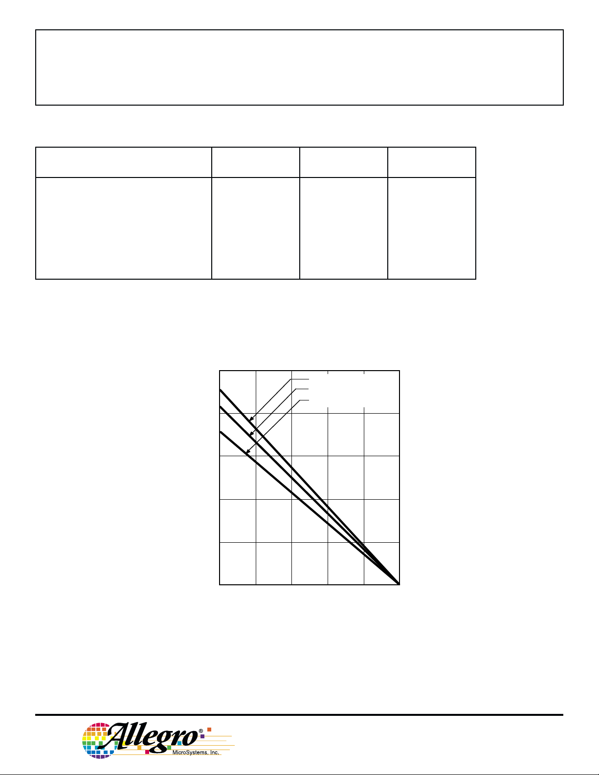
2580, 2585, AND 2588
500
500
8-CHANNEL
SOURCE DRIVERS
ALLOWABLE PEAK COLLECTOR CURRENT
AT 50°C AS A FUNCTION OF DUTY CYCLE
450
400
RECOMMENDED MAXIMUM OUTPUT CURRENT
350
300
4
250
7
200
150
100
ALLOWABLE PEAK COLLECTOR CURRENT IN mA AT 50°C
50
0
0
V = 15 V
S
10
NUMBER OF OUTPUTS
CONDUCTING
SIMULTANEOUSLY
30
20
40
PER CENT DUTY CYCLE
8
50
5
6
70
60
90
80
Dwg. No. A-11,107B
ALLOWABLE PEAK COLLECTOR CURRENT
AT 70°C AS A FUNCTION OF DUTY CYCLE
450
400
RECOMMENDED MAXIMUM OUTPUT CURRENT
350
300
250
4
5
200
150
100
ALLOWABLE PEAK COLLECTOR CURRENT IN mA AT 70°C
V = 15 V
50
S
NUMBER OF OUTPUTS
CONDUCTING
SIMULTANEOUSLY
6
7
8
3
3
100
www.allegromicro.com
0
10
0
30
20
50
40
PER CENT DUTY CYCLE
70
60
80
Dwg. No. A-11,108B
90
100
7

2580, 2585, AND 2588
8-CHANNEL
SOURCE DRIVERS
TYPICAL APPLICATIONS
COMMON-CATHODE LED DRIVER
+5 V
Dwg. No. B-1458A
Dwg. No. A-11,356
TELECOMMUNICATIONS
RELAY DRIVER
(Negative Logic)
-36 V
-48 V
V
EE
Dwg. No. A-11,362A
TELECOMMUNICATIONS RELAY DRIVER
(Positive Logic)
8
Dwg. No. A-11,363
VACUUM-FLUORESCENT DISPLAY DRIVER
(Split Supply)
115 Northeast Cutoff, Box 15036
Worcester, Massachusetts 01615-0036 (508) 853-5000

0.280
0.240
2580, 2585, AND 2588
8-CHANNEL
SOURCE DRIVERS
UDN2580A and UDN2585A
Dimensions in Inches
(controlling dimensions)
0.014
18
10
0.008
0.300
BSC
0.430
MAX
0.210
MAX
7.11
6.10
0.015
MIN
1
0.070
0.045
0.022
0.014
0.920
0.880
0.100
BSC
9
0.005
MIN
0.150
0.115
Dwg. MA-001-18A in
Dimensions in Millimeters
(for reference only)
0.355
18
1
1.77
1.15
23.37
22.35
2.54
BSC
10
9
0.13
MIN
0.204
7.62
BSC
10.92
MAX
5.33
MAX
0.39
MIN
0.558
0.356
NOTES: 1. Exact body and lead configuration at vendor’s option within limits shown.
2. Lead spacing tolerance is non-cumulative.
3. Lead thickness is measured at seating plane or below.
4. Supplied in standard sticks/tubes of 21 devices.
www.allegromicro.com
3.81
2.93
Dwg. MA-001-18A mm
9

2580, 2585, AND 2588
8-CHANNEL
SOURCE DRIVERS
A2580SLW, A2585SLW, and A2588SLW
(add “TR” to part number for tape and reel)
Dimensions in Inches
(for reference only)
20 11
0.0125
0.0091
0.2992
0.2914
0.020
0.013
0.0926
0.1043
7.60
7.40
1 2
0.0040
20
MIN.
3
0.5118
0.4961
0.050
Dimensions in Millimeters
(controlling dimensions)
11
BSC
0.419
0.394
0.050
0.016
0° TO 8°
Dwg. MA-008-20 in
0.32
0.23
10.65
10.00
0.51
0.33
2.65
2.35
1
0.10
2
MIN.
3
13.00
12.60
1.27
BSC
NOTES: 1. Exact body and lead configuration at vendor’s option within limits shown.
2. Lead spacing tolerance is non-cumulative.
3. Supplied in standard sticks/tubes of 37 devices or add “TR” to part number for tape and reel.
10
115 Northeast Cutoff, Box 15036
Worcester, Massachusetts 01615-0036 (508) 853-5000
1.27
0.40
0° TO 8°
Dwg. MA-008-20 mm

0.280
0.240
2580, 2585, AND 2588
8-CHANNEL
SOURCE DRIVERS
UDN2588A
Dimensions in Inches
(controlling dimensions)
0.014
20
11
0.008
0.300
BSC
0.430
MAX
0.210
MAX
7.11
6.10
0.015
MIN
1
0.070
0.045
0.022
0.014
1.060
0.980
0.100
BSC
10
0.005
MIN
0.150
0.115
Dwg. MA-001-20 in
Dimensions in Millimeters
(for reference only)
0.355
20
1
1.77
1.15
26.92
24.89
2.54
BSC
11
10
0.13
MIN
0.204
7.62
BSC
10.92
MAX
5.33
MAX
0.39
MIN
0.558
0.356
NOTES: 1. Exact body and lead configuration at vendor’s option within limits shown.
2. Lead spacing tolerance is non-cumulative.
3. Lead thickness is measured at seating plane or below..
4. Supplied in standard sticks/tubes of 18 devices.
www.allegromicro.com
3.81
2.93
Dwg. MA-001-20 mm
11
2580, 2585, AND 2588
8-CHANNEL
SOURCE DRIVERS
POWER SOURCE DRIVERS
IN ORDER OF 1) OUTPUT CURRENT, 2) OUTPUT VOLTAGE, 3) NUMBER OF DRIVERS
Output Ratings *
Serial Latched Diode Saturated Internal
mA V # Input Drivers Clamp Outputs Protection Part Number
-25 60 8 – X – – – 5815
60 10 X X active pull-down – – 5810-F and 6809/10
60 12 X X active pull-down – – 5811 and 6811
60 20 X X active pull-down – – 5812-F and 6812
60 32 X X active pull-down – – 5818-F and 6818
85 8 – – – – – 6118
-120 -25 8 – – X X – 2585
30 8 – – X X – 2985
50 8 X X X X – 5895
-350 35 8 – – X – X 2987
50 8 – – X – – 2981 and 2982
50 8 X X X – – 5891
-50 8 – – X – – 2580
80 8 – – X – – 2983 and 2984
80 8 X X X – – 5890
-80 8 – – X – – 2588
-500 6 1 – – – MOSFET X 2525 and 2535
6 2 – – – MOSFET X 2526 and 2536
-4000 60 4 – – X – – 2944
* Current is maximum specified test condition, voltage is maximum rating. See specification for sustaining voltage limits or
over-current protection voltage limits.
† Complete part number includes additional characters to indicate operating temperature range and package style.
Features
†
12
The products described here are manufactured under one or more
U.S. patents or U.S. patents pending.
Allegro MicroSystems, Inc. reserves the right to make, from time to
time, such departures from the detail specifications as may be
required to permit improvements in the performance, reliability, or
manufacturability of its products. Before placing an order, the user is
cautioned to verify that the information being relied upon is current.
Allegro products are not authorized for use as critical components
in life-support devices or systems without express written approval.
The information included herein is believed to be accurate and
reliable. However, Allegro MicroSystems, Inc. assumes no responsibility for its use; nor for any infringement of patents or other rights of
third parties which may result from its use.
115 Northeast Cutoff, Box 15036
Worcester, Massachusetts 01615-0036 (508) 853-5000
 Loading...