

ALLEGRO 2526, 2536 DATA SHEET
查询2526供应商
USB DUAL POWER CONTROL SWITCHES
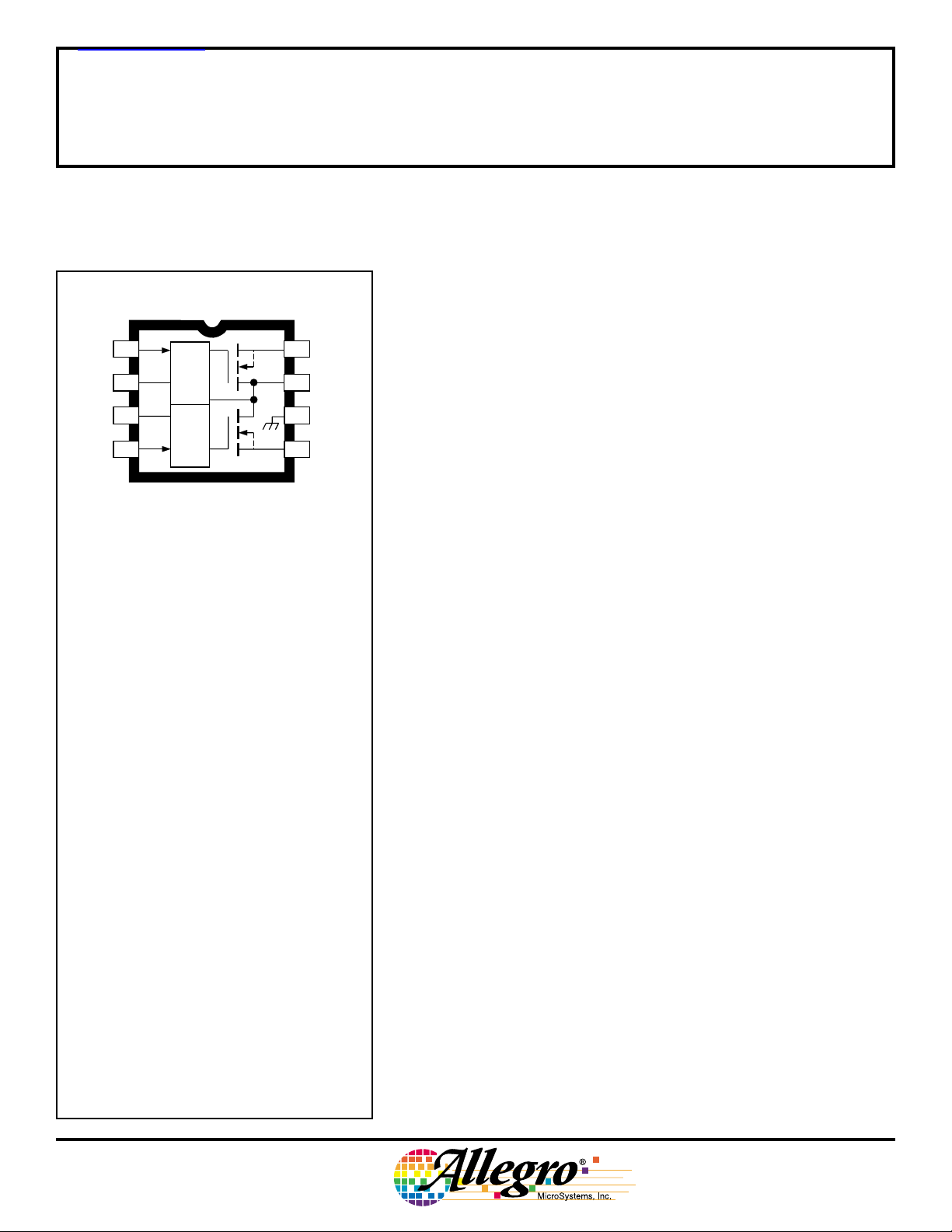
A2526EM
EN
FLG
FLG
EN
Note that the A2526EM (DIP) and the
A2526EL (SOIC) are electrically identical and
share a common terminal number assignment.
1
A
2
A
3
B
45
B
GATE
CONTROL
GATE
CONTROL
ADVANCE INFORMATION
(subject to change without notice)
March 5, 1999
ABSOLUTE MAXIMUM RATINGS
Supply Voltage, V
Output Voltage, V
Output Current,
I
................. Internally Limited
OUT
ENABLE Voltage Range,
......................... –0.3 V to 10 V
V
EN
Fault Flag Voltage, V
Fault Flag Current, I
Package Power Dissipation,
................................. See Graph
P
D
Operating Temperature Range,
......................... -40°C to +85°C
T
A
Junction Temperature, T
Storage Temperature Range,
T
........................... -65°C to 150°C
S
* Fault conditions that produce excessive
junction temperature will activate device
thermal shutdown circuitry. These conditions
can be tolerated but should be avoided.
..................... 6.0 V
IN
................... 6.0 V
OUT
FLG
............. 50 mA
FLG
J
8
OUT
7
IN
GND
6
OUT
Dwg. PP-070-2
.............. 8.0 V
....... +150°C*
2526
AND
Data Sheet
27447.2
2536
The A2526EL/M and A2536EL/M are integrated high-side dual
power switches, optimized for self-powered and bus-powered Universal Serial Bus (USB) applications. Few external components are
A
B
necessary to satisfy USB requirements. The A2526EL/EM ENABLE
inputs are active high; the A2536EL/EM are active low.
All devices are ideally suited for USB applications. Each switch
channel supplies up to 500 mA as required by USB peripheral devices.
In addition, the switch’s low on-resistance permits achieving the USB
voltage-drop requirements. Fault current is limited to typically
750 mA, satisfying the UL 25 VA safety requirements, and a flag
output is available to indicate a fault condition to the local USB
controller. Momentary voltage drops that may occur on the upstream
port when the switch is enabled in bus-powered applications is eliminated by a “soft start” feature.
Additional features include thermal shutdown to prevent catastrophic
switch failure from high-current loads, undervoltage lockout to ensure
that the device remains OFF unless there is a valid input voltage
present, and 3.3 V and 5 V logic-compatible enable inputs.
These switches are provided in 8-pin mini-DIP (suffix ‘M’) and
8-lead SOIC (suffix ‘L’) packages.
Features
■ 2.7 V to 5.8 V Input
■ Up to 500 mA Continuous Load Current per Port
■ 140 mΩ Maximum ON-Resistance
■ 1.25 A Maximum Short-Circuit Current Limit
■ Individual Open-Drain Fault Flag Outputs
■ 110 µA Typical ON-State Supply Current
■ 1 µA Typical OFF-State Supply Current
■ Outputs Can be Forced Higher Than Input (off-state)
■ Thermal Shutdown
■ 2.4 V Typical Undervoltage Lockout
■ 1 ms Turn On (soft-start) and Fast Turn Off
■ Active-High or Active-Low Enable Versions
■ Improved Replacements for MIC2526-1 and MIC2526-2
Applications
■ USB Hosts and Self-Powered Hubs
■ USB Bus-Powered Hubs
■ Hot Plug-In Power Supplies
■ Battery-Charger Circuits
2526
AND
2536
USB
DUAL POWER CONTROL
SWITCHES
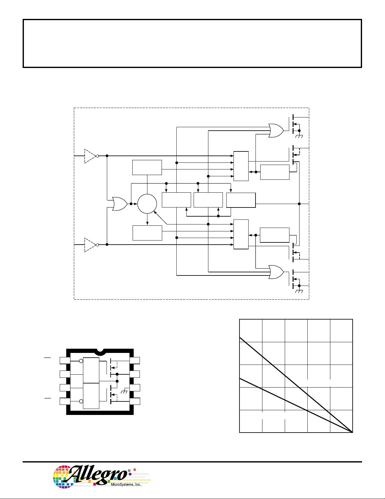
FUNCTIONAL BLOCK DIAGRAM
FLG
A
EN
EN
A2536 ONLY
A
A2536 ONLY
B
CHARGE
PUMP
OSC
CHARGE
PUMP
TSD
UVLO
1.2 V
REF.
2.5
GATE
CONTROL
GATE
CONTROL
CURRENT
LIMIT
CURRENT
LIMIT
OUT
IN
OUT
FLG
GND
Dwg. FP-049-1
A
B
B
A2536EM
EN
FLG
FLG
EN
1
A
2
A
3
B
45
B
GATE
CONTROL
GATE
CONTROL
Note that the A2536EM (DIP) and the
A2536EL (SOIC) are electrically identical and
share a common terminal number assignment.
8
OUT
IN
7
GND
6
OUT
Dwg. PP-070-3
2.0
A
B
1.5
1.0
0.5
0
ALLOWABLE PACKAGE POWER DISSIPATION IN WATTS
SUFFIX 'L', R
25
50 75 100 125 150
AMBIENT TEMPERATURE IN °C
115 Northeast Cutoff, Box 15036
Worcester, Massachusetts 01615-0036 (508) 853-5000
Copyright © 1999, Allegro MicroSystems, Inc.
θJA
= 108°C/W
SUFFIX 'M', R
θJA
= 60°C/W
Dwg. GP-009-2

2526
AND
2536
USB
DUAL POWER CONTROL
SWITCHES
Electrical Characteristics at T
= 25°C, V
A
= 5 V (unless otherwise noted).
IN
Limits
Parameter Test Conditions Min Typ Max Units
Operating Voltage Range V
IN
Switch Resistance VIN = 5 V, I
= 500 mA – 100 140 mΩ
OUT
2.7 – 5.8 V
VIN = 3.3 V, IOUT = 500 mA – 100 140 mΩ
Output Leakage Current Each output (output disabled), VIN = 5 V, V
= 0 – – 10 µA
OUT
Maximum Load Current Each output 500 – – mA
Short-Circuit Current Limit Each output (enable into load), V
Current-Limit Threshold Ramped load applied to enabled output, V
= 4 V 0.5 – 1.25 A
OUT
≤ 4 V – 1.6 – A
OUT
ENABLE Input Threshold Low-to-high transition – 2.1 2.4 V
High-to-low transition 0.8 1.9 – V
ENABLE Input Hysteresis – 0.2 – V
ENABLE Input Current V
= 0 V to 5.5 V – ±0.01 ±1.0 µA
EN
ENABLE Input Cap. – 1.0 – pF
Output Turn-On Delay R
Output Turn-On Rise Time R
Output Turnoff Delay R
Output Turnoff Fall Time R
Error Flag Output VIN = 5 V, I
Resistance
Error Flag Off Current V
= 10Ω, each output – 0.5 – ms
L
= 10Ω each output – 1.0 – ms
L
= 10Ω each output – 1.0 – µs
L
= 10Ω each output – 1.0 – µs
L
= 10 mA – 10 – Ω
L
VIN = 3.3 V, I
= 5 V – 0.01 – µA
FLG
= 10 mA – 15 – Ω
L
Supply Current Both switches OFF (see note), OUT = open – 0.75 5.0 µA
Both switches ON (see note), OUT = open – 110 160 µA
UVLO Threshold Increasing V
Decreasing V
Over-Temperature Increasing T
Shutdown Threshold
Decreasing T
IN
IN
J
J
– 2.5 – V
– 2.3 – V
– 165 – °C
– 155 – °C
Note — OFF is ≤ 0.8 V and ON is ≥ 2.4 V (active high) for the A2526EL/EM. OFF is ≥ 2.4 V and ON is ≤ 0.8 V (active low) for
the A2536EL/EM.
 Loading...