

查询2526供应商
USB DUAL POWER CONTROL SWITCHES
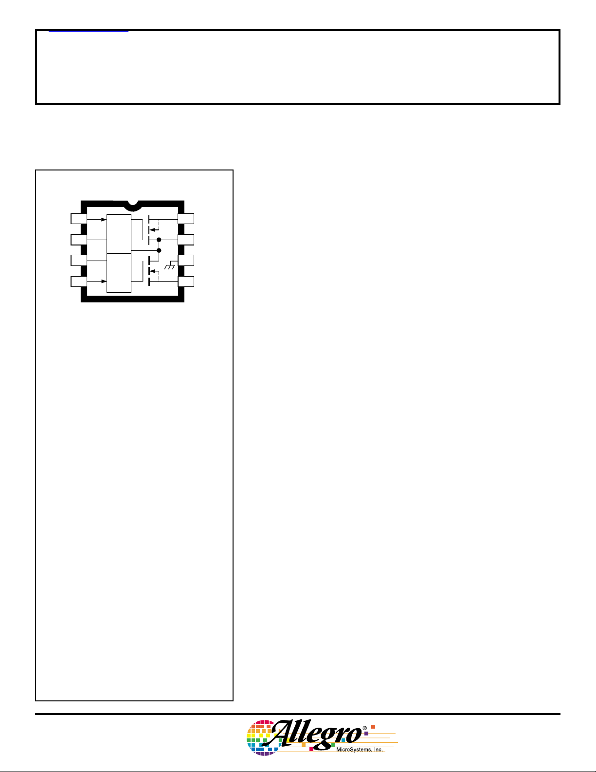
A2526EM
EN
FLG
FLG
EN
Note that the A2526EM (DIP) and the
A2526EL (SOIC) are electrically identical and
share a common terminal number assignment.
1
A
2
A
3
B
45
B
GATE
CONTROL
GATE
CONTROL
ADVANCE INFORMATION
(subject to change without notice)
March 5, 1999
ABSOLUTE MAXIMUM RATINGS
Supply Voltage, V
Output Voltage, V
Output Current,
I
................. Internally Limited
OUT
ENABLE Voltage Range,
......................... –0.3 V to 10 V
V
EN
Fault Flag Voltage, V
Fault Flag Current, I
Package Power Dissipation,
................................. See Graph
P
D
Operating Temperature Range,
......................... -40°C to +85°C
T
A
Junction Temperature, T
Storage Temperature Range,
T
........................... -65°C to 150°C
S
* Fault conditions that produce excessive
junction temperature will activate device
thermal shutdown circuitry. These conditions
can be tolerated but should be avoided.
..................... 6.0 V
IN
................... 6.0 V
OUT
FLG
............. 50 mA
FLG
J
8
OUT
7
IN
GND
6
OUT
Dwg. PP-070-2
.............. 8.0 V
....... +150°C*
2526
AND
Data Sheet
27447.2
2536
The A2526EL/M and A2536EL/M are integrated high-side dual
power switches, optimized for self-powered and bus-powered Universal Serial Bus (USB) applications. Few external components are
A
B
necessary to satisfy USB requirements. The A2526EL/EM ENABLE
inputs are active high; the A2536EL/EM are active low.
All devices are ideally suited for USB applications. Each switch
channel supplies up to 500 mA as required by USB peripheral devices.
In addition, the switch’s low on-resistance permits achieving the USB
voltage-drop requirements. Fault current is limited to typically
750 mA, satisfying the UL 25 VA safety requirements, and a flag
output is available to indicate a fault condition to the local USB
controller. Momentary voltage drops that may occur on the upstream
port when the switch is enabled in bus-powered applications is eliminated by a “soft start” feature.
Additional features include thermal shutdown to prevent catastrophic
switch failure from high-current loads, undervoltage lockout to ensure
that the device remains OFF unless there is a valid input voltage
present, and 3.3 V and 5 V logic-compatible enable inputs.
These switches are provided in 8-pin mini-DIP (suffix ‘M’) and
8-lead SOIC (suffix ‘L’) packages.
Features
■ 2.7 V to 5.8 V Input
■ Up to 500 mA Continuous Load Current per Port
■ 140 mΩ Maximum ON-Resistance
■ 1.25 A Maximum Short-Circuit Current Limit
■ Individual Open-Drain Fault Flag Outputs
■ 110 µA Typical ON-State Supply Current
■ 1 µA Typical OFF-State Supply Current
■ Outputs Can be Forced Higher Than Input (off-state)
■ Thermal Shutdown
■ 2.4 V Typical Undervoltage Lockout
■ 1 ms Turn On (soft-start) and Fast Turn Off
■ Active-High or Active-Low Enable Versions
■ Improved Replacements for MIC2526-1 and MIC2526-2
Applications
■ USB Hosts and Self-Powered Hubs
■ USB Bus-Powered Hubs
■ Hot Plug-In Power Supplies
■ Battery-Charger Circuits
2526
AND
2536
USB
DUAL POWER CONTROL
SWITCHES
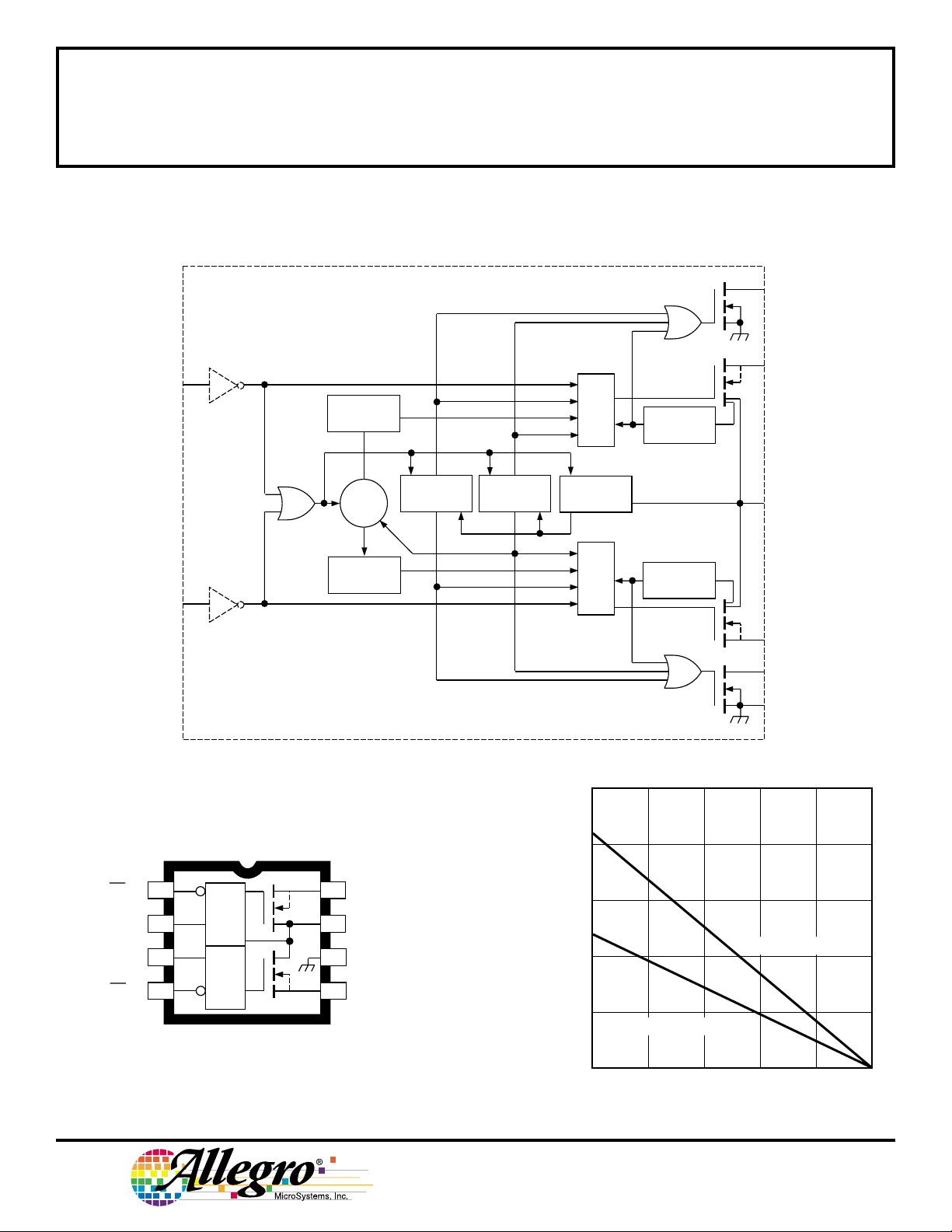
FUNCTIONAL BLOCK DIAGRAM
FLG
A
EN
EN
A2536 ONLY
A
A2536 ONLY
B
CHARGE
PUMP
OSC
CHARGE
PUMP
TSD
UVLO
1.2 V
REF.
2.5
GATE
CONTROL
GATE
CONTROL
CURRENT
LIMIT
CURRENT
LIMIT
OUT
IN
OUT
FLG
GND
Dwg. FP-049-1
A
B
B
A2536EM
EN
FLG
FLG
EN
1
A
2
A
3
B
45
B
GATE
CONTROL
GATE
CONTROL
Note that the A2536EM (DIP) and the
A2536EL (SOIC) are electrically identical and
share a common terminal number assignment.
8
OUT
IN
7
GND
6
OUT
Dwg. PP-070-3
2.0
A
B
1.5
1.0
0.5
0
ALLOWABLE PACKAGE POWER DISSIPATION IN WATTS
SUFFIX 'L', R
25
50 75 100 125 150
AMBIENT TEMPERATURE IN °C
115 Northeast Cutoff, Box 15036
Worcester, Massachusetts 01615-0036 (508) 853-5000
Copyright © 1999, Allegro MicroSystems, Inc.
θJA
= 108°C/W
SUFFIX 'M', R
θJA
= 60°C/W
Dwg. GP-009-2

2526
AND
2536
USB
DUAL POWER CONTROL
SWITCHES
Electrical Characteristics at T
= 25°C, V
A
= 5 V (unless otherwise noted).
IN
Limits
Parameter Test Conditions Min Typ Max Units
Operating Voltage Range V
IN
Switch Resistance VIN = 5 V, I
= 500 mA – 100 140 mΩ
OUT
2.7 – 5.8 V
VIN = 3.3 V, IOUT = 500 mA – 100 140 mΩ
Output Leakage Current Each output (output disabled), VIN = 5 V, V
= 0 – – 10 µA
OUT
Maximum Load Current Each output 500 – – mA
Short-Circuit Current Limit Each output (enable into load), V
Current-Limit Threshold Ramped load applied to enabled output, V
= 4 V 0.5 – 1.25 A
OUT
≤ 4 V – 1.6 – A
OUT
ENABLE Input Threshold Low-to-high transition – 2.1 2.4 V
High-to-low transition 0.8 1.9 – V
ENABLE Input Hysteresis – 0.2 – V
ENABLE Input Current V
= 0 V to 5.5 V – ±0.01 ±1.0 µA
EN
ENABLE Input Cap. – 1.0 – pF
Output Turn-On Delay R
Output Turn-On Rise Time R
Output Turnoff Delay R
Output Turnoff Fall Time R
Error Flag Output VIN = 5 V, I
Resistance
Error Flag Off Current V
= 10Ω, each output – 0.5 – ms
L
= 10Ω each output – 1.0 – ms
L
= 10Ω each output – 1.0 – µs
L
= 10Ω each output – 1.0 – µs
L
= 10 mA – 10 – Ω
L
VIN = 3.3 V, I
= 5 V – 0.01 – µA
FLG
= 10 mA – 15 – Ω
L
Supply Current Both switches OFF (see note), OUT = open – 0.75 5.0 µA
Both switches ON (see note), OUT = open – 110 160 µA
UVLO Threshold Increasing V
Decreasing V
Over-Temperature Increasing T
Shutdown Threshold
Decreasing T
IN
IN
J
J
– 2.5 – V
– 2.3 – V
– 165 – °C
– 155 – °C
Note — OFF is ≤ 0.8 V and ON is ≥ 2.4 V (active high) for the A2526EL/EM. OFF is ≥ 2.4 V and ON is ≤ 0.8 V (active low) for
the A2536EL/EM.

2526
AND
2536
USB
DUAL POWER CONTROL
SWITCHES
FUNCTIONAL DESCRIPTION
Power switch
The power switch is an N-channel MOSFET with a maximum
on-state resistance of 140 mΩ (VIN = 5 V). Configured as a
high-side switch, the power switch prevents current flow in
either direction if disabled. The drain body diode is disconnected from the source when the switch is OFF allowing the
output voltage to exceed the input voltage without causing
current conduction. The power switch supplies a minimum of
500 mA per switch.
Charge pump
An internal charge pump supplies power to the driver circuit
and provides the necessary voltage to pull the gate of the
MOSFET above the source. The charge pump operates from
input voltages as low as 2.7 V. The charge pump is limited to
2.5 µA to establish a controlled turn on time of typically 1 ms.
Driver
The driver controls the gate voltage of the power switch. To
limit large current surges and reduce the associated electromagnetic interference (EMI) produced, the driver incorporates
circuitry that controls the rise times and fall times of the output
voltage. The rise time is typically 1 ms.
ENABLE (EN or EN)
Fault Flag (FLG)
This open drain output is asserted (active low) when an
overcurrent or over temperature condition is encountered. The
output will remain asserted until the overcurrent or over
temperature condition is removed.
Current sense
A sense FET monitors the current supplied to the load. The
sense FET measures current more efficiently than conventional
resistance methods. When an overload or short circuit is
encountered, the current-sense circuitry sends a control signal to
the driver. The driver in turn reduces the gate voltage and
drives the power FET into its saturation region, which switches
the output into a constant-current mode and holds the current
constant while varying the voltage on the load.
Thermal sense
An internal thermal-sense circuit shuts off the power switch
when the junction temperature rises to approximately 165°C.
Hysteresis is built into the thermal sense circuit. After the
device has cooled approximately 10°C, the switch turns back
ON. The switch continues to cycle off and on until the fault is
removed.
Undervoltage lockout
The logic enable disables the power switch and the bias for the
charge pump, driver, and other circuitry to reduce the supply
current to less than 5 µA maximum when a logic high is present
on EN (A2526) or a logic low is present (A2536). The proper
logic level restores bias to the drive and control circuits and
turns the power ON. The enable input is a compatible with both
TTL and CMOS logic levels.
115 Northeast Cutoff, Box 15036
Worcester, Massachusetts 01615-0036 (508) 853-5000
A voltage-sense circuit monitors the input voltage. When the
input voltage is approximately 2 V, a control signal turns OFF
the power switch.

DUAL POWER CONTROL
APPLICATIONS INFORMATION
2526
AND
2536
USB
SWITCHES
Overcurrent
A sense FET is employed for overcurrent conditions. Unlike
current-sense resistors, sense FETs do not increase the series
resistance of the current path. When an overcurrent condition is
detected, the device maintains a constant output current and
reduces the output voltage accordingly. Complete shutdown
occurs only if the fault is present long enough to activate
thermal limiting.
Three possible overload conditions can occur. In the first
condition, the output has been shorted before the device is
enabled or between VIN has been applied. The device senses
the short and immediately switches into a constant-current
output.
In the second condition, the short occurs while the device is
enabled. At the instant the short occurs, very high currents may
flow for a short time before the current-limit circuit can react .
After the current-limit circuit has tripped (reached the
overcurrent trip threshold) the device switches into constantcurrent mode.
In the third condition, the load has been gradually increased
beyond the recommended operating current. The current is
permitted to rise until the current-limit threshold is reached or
until the thermal limit of the device is exceeded. The device is
capable of delivering current up to the current-limit threshold
without damage. Once the threshold has been reached, the
device switches into its constant-current mode.
Fault Flag (FLG)
The FLG open-drain output is asserted (active low) when an
overcurrent or over-temperature condition is encountered. The
output will remain asserted until the overcurrent or overtemperature condition is removed. Connecting a heavy
capacitive load to an enabled device can cause momentary false
over-current reporting from the inrush current flowing through
the device, charging the downstream capacitor. An RC filter
can be connected to the terminal to reduce false overcurrent
reporting. Using low-ESR electrolytic capacitors on the output
lowers the inrush current flow through the device during hotplug events by providing a low impedance energy source,
thereby reducing erroneous overcurrent reporting.
Power dissipation and junction temperature
The low on-resistance of the n-channel MOSFET allows small
surface-mount packages, such as an SOIC, to pass large
currents. The thermal resistance of these packages are high
compared to those of power packages; it is good design practice
to check power dissipation and junction temperature. The first
step is to find r
ture. Next, calculate the power dissipation using:
PD = r
DS(on)
Finally, calculate the junction temperature:
TJ = PD x R
where:
TA = ambient temperature °C
R
= thermal resistance (
θJA
Thermal protection
Thermal protection prevents damage to the IC when heavyoverload or short-circuit faults are present for extended periods
of time. The faults force these devices into constant-current
mode, which causes the voltage across the high-side switch to
increase; under short-circuit conditions, the voltage across the
switch is equal to the input voltage. The increased dissipation
causes the junction temperature to rise to high levels. The
protection circuit senses the junction temperature of the switch
and shuts it OFF. Hysteresis is built into the thermal sense
circuit, and after the device has cooled approximately 20°, the
switch turns back ON. The switch continues to cycle in this
manner until the load fault or input power is removed.
Undervoltage lock-out (UVLO)
An undervoltage lockout ensures that the power switch is in the
OFF state at power up. Whenever the input voltage falls below
approximately 2 V, the power switch will be quickly turned
OFF. This facilitates the design of hot-insertion systems where
it is not possible to turn OFF the power switch before input
power is removed. The UVLO will also keep the switch from
being turned ON until the power supply has reached at least
2 V, even if the switch is enabled. Upon reinsertion, the power
switch will be turned ON, with a controlled rise time to reduce
EMI and voltage overshoots.
Power supply considerations
A 0.1 µF ceramic bypass capacitor between IN and GND, close
to the device, is recommended. Placing a high-value electrolytic capacitor on the output terminals is also desirable when the
output load is heavy. The capacitor reduces power supply
transients that may cause ringing on the input. Also, bypassing
the output with a 0.01 µF to 0.1 µF ceramic capacitor improves
the immunity of the device to short-circuit transients.
at the input voltage and operating tempera-
DS(on)
2
x I
+ T
θJA
A
SOIC = 108°C/W, DIP = 60°C/W
).
2526
AND
2536
USB
DUAL POWER CONTROL
SWITCHES
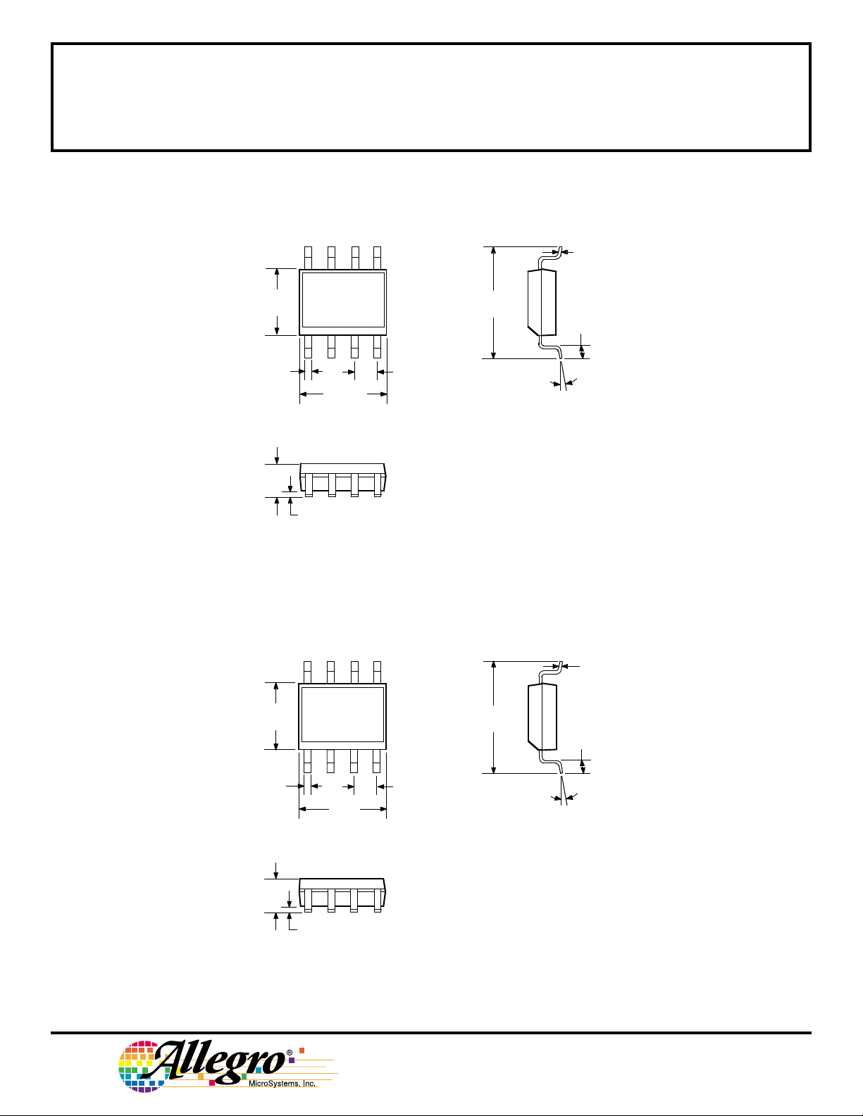
A2526EL and A2536EL
Dimensions in Inches
(for reference only)
0.1574
0.1497
0.020
0.013
0.0688
0.0532
8
1
0.1968
0.1890
0.0040
0.2440
0.2284
0.050
BSC
MIN.
Dimensions in Millimeters
(controlling dimensions)
0.0098
0.0075
0.050
0.016
0° TO 8°
Dwg. MA-007-8 in
8
4.00
3.80
0.51
1
0.33
1.75
1.35
0.10
NOTES: 1. Lead spacing tolerance is non-cumulative.
2. Exact body and lead configuration at vendor’s option within limits shown.
6.20
5.80
1.27
5.00
BSC
4.80
MIN.
115 Northeast Cutoff, Box 15036
Worcester, Massachusetts 01615-0036 (508) 853-5000
0° TO 8°
Dwg. MA-007-8 mm
0.25
0.19
1.27
0.40

0.280
0.240
A2526EM and A2536EM
Dimensions in Inches
(controlling dimensions)
0.014
58
0.008
2526
AND
2536
USB
DUAL POWER CONTROL
SWITCHES
0.430
MAX
0.300
BSC
0.210
MAX
7.11
6.10
0.015
MIN
1
0.070
0.045
8
1
1.77
1.15
0.022
0.014
0.400
0.355
10.16
9.02
4
0.005
MIN
0.150
0.115
0.100
BSC
Dimensions in Millimeters
(for reference only)
5
4
0.13
MIN
0.355
0.204
Dwg. MA-001-8A in
10.92
MAX
7.62
BSC
5.33
MAX
0.39
MIN
0.558
0.356
2.54
BSC
3.81
2.93
NOTES: 1. Leads 1, 4, 5, and 8 may be half leads at vendor’s option.
2. Lead thickness is measured at seating plane or below.
3. Lead spacing tolerance is non-cumulative.
4. Exact body and lead configuration at vendor’s option within limits shown.
Dwg. MA-001-8A mm

2526
AND
2536
USB
DUAL POWER CONTROL
SWITCHES
Allegro MicroSystems, Inc. reserves the right to make,
from time to time, such departures from the detail specifications as may be required to permit improvements in the
design of its products.
The information included herein is believed to be
accurate and reliable. However, Allegro MicroSystems, Inc.
assumes no responsibility for its use; nor for any infringements of patents or other rights of third parties which may
result from its use.
115 Northeast Cutoff, Box 15036
Worcester, Massachusetts 01615-0036 (508) 853-5000
 Loading...