

Page 1
DJ-493
DJ-496/438
Servic e Man ua l
CONTENTS
SPECIFICATIONS
1) G E NE R AL.............................................................................2
2) TRANSM ITTER...................................................................2
3) RECE IVER............................................................................2
CIRCUIT DESCRIPTION
1) Receiver Sy s tem ............................................................3, 4
2) Transmitter S ystem.............................................................4
3) PLL Synthesizer Circuit
4) CPU and Peripheral C ircuits
5) M 38267M8L252GP (X A 0725)..................................... 6 - 8
SEMICONDUCTOR DATA
1) NMJ2070M T 1 (XA0210) ..................................................9
2) AT24C16N-10SI-2.7TER (X A 0368)................................9
3) M 5222FP-600C (XA0385)
4) TK14521MTL (X A 0515).................................................. 11
5) M64076AGP (XA0352)
6 ) NJM2904V-TE1 (XA0573) ............................................. 12
7) NJM2902V-TE1 (XA0596) ............................................. 12
8 ) S-81350HG-KD-T1 (XA0724) ....................................... 13
9) S-80845ALM P-EA9-T2 (XA0620) ................................ 13
10) 2SK2975 (XE00 38)........................................................... 13
11) Transistor, Diode, and LED Ontline Drawings
12) LCD Connection (EL0044)............................................ 14
...............................................
......................................
.............................................
................................................... 12
4, 5
5, 6
...........
10
14
EXPLODED VIEW
1) Front V iew............................................................................15
2) R earVie w ............................................................................16
PARTS LIST (DJ-493)
MAIN U nit
Mechanical P a rts..............................................................22
Packing P arts......................................................................22
PARTS LIST (DJ-496)
MAIN U n it.....................................................................23-27
Mechanical Pa rts...............................................................28
Packing P arts......................................................................28
ADJUSTMENT
1) Required Test E quipm ent
2) Adjustment M ode
PC BOARD VIEW
MAIN U n it.....................................................................35, 36
SCHEMATIC DIAGRAM
BLOCK DIAGRAM
.................................................................... 17-21
........................................
.......................................................31-34
.............................................
........................................................
29, 30
37, 38
39, 40
SNCO, inc.
Page 2
SPECIFICATIONS
1) GENERAL
Frequency coverage
Mode
Channel steps
Memory channels
Antenna connector
Frequency stability
Microphone input impedance
Power supply requirement
Current drain (at 13.8 V DC)
Usable temperature range
Dimensions
(Projections not included)
Weight
DTMF (DJ-496)
Sub audible Tone(CTCSS)
Sub audible Tone (DCS)
DJ-493T
DJ-496T
DJ-438TA2
F3E (FM)
5,10,12.5,15,20,25, & 30kHz
40channels+1 CALL channel
BNC (50Q unbalanced)
±5 ppm
2kfi nominal
7.0 - 16.0V DC (negative ground)
1.4A (typical) Transmit high at 5W
200mA (typical) Receive at 280mW
50mA (typical) standby
20mA (typical) Battery save on
-10 ~ +60°C (14 ~ 140°F)
56 (W) x 124 (H) x 40 (D) mm (with EBP-48N)
2.2"(W) x 4.88"(H) x 1,57"(D) inches (with EBP-48N)
Approx. 375g (13.2oz) (with EBP-48N)
16 Buttons Keypad
encoder/decoder installed (39tones)
encoder/decoder installed (104codes)
TX 430 ~ 449.995MHz RX 430 ~ 449.995MHz
E
TX 430 - 439.995MHz RX 430 ~ 439.995MHz
TA2
TX 450 ~ 469.995MHz RX 450 ~ 469.995MHz
TX 430 ~ 449.995MHz RX 430 ~ 449.995MHz
E
TX 430 ~ 439.995MHz RX 430 ~ 439.995MHz
TX 450 ~ 469.995MHz RX 450 ~ 469.995MHz
2) TRANSMITTER
Output power
Modulation system
Spurious emissions
Max. frequency deviation
3) RECEIVER
Receive system
Intermediate frequencies
Sensitivity(12dB SINAD)
Selectivity
Audio output power
2
Approx. 4W EBP-48N installed
Approx. 5W 13.8V DC
Approx. 0.8W (LOW)
Variable reactance frequency modulation
Less than -60dB
±5 kHz
Double conversion superheterodyne
1st 45.1 MHz/2nd 455kHz
Less than -12.0dB|x (0.25V)
-6dB :12kHz or more
-60dB : 26kHz or less
280mW (typical with an 8Q load)
200mW (8i3 10% THD)
Page 3
CIRCUIT DESCRIPTION
1) Receiver System
The receiver system is a double superheterodyne system with a 45.1 MHz first IF and a 455kHz second IF.
1. Front End
The received signal at any frequency in the 430.00- to 449.995-MHz range is
passed through the low-pass filter (L2, L3, L8, C2, C9, C10, C11, and C62)
and high-pass filter (C56, C57, C61, L25 and D25), and amplified by the RF
amplifier (Q9). The signal from Q9 is then passed through the tuning circuit
(L19, L20, L21 and varicaps D12, D13 and D14) and converted into 45.1MHz
by the mixer (Q10). The tuning circuit, which consists of L25, L19, L20, L21,
D15, D12, D13 and D14 is controlled by the tracking voltage form the CPU so
that it is optimized for the reception frequency. The local signal from the VCO
is passed through the buffer (Q11), and supplied to the source of the mixer
(Q10). The radio uses the lower side of the superheterodyne system.
2. IF Circuit
The mixer mixes the received signal with the local signal to obtain the sum of
and difference between them. The crystal filter (XF1) selects 45.1MHz fre
quency from the results and eliminates the signals of the unwanted frequen
cies. The first IF amplifier (Q8) then amplifies the signal of the selected fre
quency.
3. Demodulator Circuit
4. Audio Circuit
After the signal is amplified by the first IF amplifier (Q8), it is input to pin 16 of
the demodulator IC (IC4). The second local signal of 45.555MHz, which is
oscillated by the internal oscillation circuit in IC4 and crystal (X2). Then, these
two signals are mixed by the internal mixer in IC4 and the result is converted
into the second IF signal with a frequency of 455kHz. The second IF signal is
output from pin 3 of IC4 to the ceramic filter (FL1), where the unwanted fre
quency band of that signal is eliminated, and the resulting signal is sent back
to the IC4 through pin 5.
The second IF signal input via pin 5 is demodulated by the internal limiter
amplifier and quadrature detection circuit in IC4, and output as an audio signal
through pin 10.
The audio signal from pin 10 of IC4 is compensated to the audio frequency
characteristics in the de-emphasis circuit (R106, R107, C128, C127) and am
plified by the AF amplifier (Q27). The signal is then input to pin 2 of the elec
tronic volume (IC6) for volume adjustment, and output from pin 1. The ad
justed signal is sent to the audio power amplifier (IC5) through pin 2 to drive
the speaker.
3
Page 4
5. Squelch Circuit
2) Transmitter System
1. Modulator Circuit
2. Power Amplifier Circuit
The signal except for the noise component in AF signal of 104 is cut by the
active filter inside 1C. The noise component is amplified and rectified, then
converted to the DC voltage to output from pin13 of IC4. The voltage is led to
pin 2 of CPU and compared with the setting voltage. The squelch will open if
the input voltage is lower than the setting voltage.
The audio signal is converted to an electric signal in either the internal or
external microphone, and input to the microphone amplifier (IC8). IC8 con
sists of two operational amplifiers; one amplifier (pins 5, 6, and 7) is composed
of pre-emphasis and IDC circuits and the other (pins 1, 2, and 3) is composed
of a splatter filter. The maximum frequency deviation is obtained by VR1 and
input to the cathode of the varicap of the VCO, to change the electric capacity
in the oscillation circuit. This produces the frequency modulation.
The transmitted signal is oscillated by the VCO, amplified by the pre-drive IC
(IC1) and drive amplifier (04), and input to the final amplifier (02). The signal
is then amplified by the final amplifier (02) and led to the antenna switch (D2)
and low-pass filter (L5, L3,12, C24, C11, 010, and C9), where unwanted high
harmonic waves are reduced as needed, and the resulting signal is supplied
to the antenna.
3. APC Circuit
Part of the transmission power from the low-pass filter is detected by D7, con
verted to DC, and then amplified by a differential amplifier. The output voltage
controls the bias voitage from the source of 02 and 04 to maintain the trans
mission power constant.
3) PLL Synthesizer Circuit
1. PLL
The dividing ratio is obtained by sending data from the CPU (IC9) to pin 2 and
sending clock pulses to pin 3 of the PLL IC (IC2). The oscillated signal from the
VCO is amplified by the buffer (05, 037) and input to pin 6 of IC2. Each
programmable divider in IC2 divides the frequency of the input signal by N
according to the frequency data, to generate a comparison frequency of 5 or
6.25kHz.
2. Reference Frequency Circuit
The reference frequency appropriate for the channel steps is obtained by di
viding the 21,25MHz reference oscillation (X1) by 4250 or 3400, according to
the data from the CPU (IC9). When the resulting frequency is 5kHz, channel
steps of 5, 10, 15, 20, 25, 30, and 50kHz are used. When it is 6.25kHz, the
4 12.5kHz channel step is used.
Page 5
3. Phase Comparator Circuit
The PLL (IC2) uses the reference frequency, 5 or 6.25kHz. The phase com
parator in the IC2 compares the phase of the frequency from the VCO with
that of the comparison frequency, 5 or 6.25kHz, which is obtained by the inter
nal divider in IC2.
4. PLL Loop Filter Circuit
If a phase difference is found in the phase comparison between the reference
frequency and VCO output frequency, the charge pump output (pin 8) of IC2
generates a pulse signal, which is converted to DC voltage by the PLL loop
filter and input to the varicap of the VCO unit for oscillation frequency control.
5. VCO Circuit
A Colpitts oscillation circuit driven by Q3 directly oscillates the desired fre
quency. The frequency control voltage determined in the CPU (IC9) and PLL
circuit is input to the varicaps (D3). This change the oscillation frequency, which
is amplified by the VCO buffer (Q5) and output from the VCO unit.
4) CPU and Peripheral Circuits
1. LCD Display Circuit
The CPU turns ON the LCD via segment and common terminals with 1/4 the
duty and 1/4 the bias, at the frame frequency is 112.5Hz.
2. Display Lamp Circuit
When the LAMP key is pressed, “H” is output form pin 42 of CPU (IC9) to the
bases of Q19, Q24 and Q25.
3. Reset and Backup
When the power form the DC jack or external battery increases from Circuits 0
V to 2.5V or more, “H” level reset signal is output from the reset IC (IC11) to pin
33 of the CPU (IC9), causing the CPU to reset. The reset signal, however,
waits at 100, and does not enter the CPU until the CPU clock (X3) has stabi
lized.
4. S(Signal) Meter Circuit
The DC potential of pin 8 of iC4 is input to pin 1 of the CPU (IC9), converted
from an analog to a digital signal, and displayed as the S-meter signal on the
LCD.
5. DTMF Encoder (DJ-496)
The CPU (IC9) is equipped with an internal DTMF encoder. The DTMF signal
is output from pin 10, through R179 and R180 (for level adjust-ment), and then
through the microphone amplifier (IC8), and is sent to the varicap of the VCO
for modulation. At the same time, the monitor-ing tone passes through the AF
circuit and is output form the speaker.
Page 6
6. CTCSS Encoder
7. DCS Encoder
8. CTCSS, DCS Decoder
9. Clock Shift
The CPU (IC9) is equipped with an internal tone encoder. The tone signal
(67.0 to 250.3 Hz) is output from pin 9 of the CPU to the varicap (D4) of the
The CPU (IC9) is equipped with an internal DCS code encoder. The code (023
to 754) is output from pin 9 of the CPU to the varicap (D16) of the PLL refer
ence oscillator. When DCS is ON, DCS MUTE circuit (Q12-ON, Q18-ON, 015-
OFF) works. The modulation activates in X1 side only.
The voice band of the AF output signal from pin 10 of IC4 is cut by sharp active
filter IC7 (VCVS) and amplified, then led to pin 4 of CPU. The input signal is
compared with the programmed tone frequency code in the CPU. The squelch
will open when they match.
In the unlikely event that CPU clock noise is present on a particular operating
frequency programmed into the radio, you can shift the CPU clock frequency
to avoid the CPU clock-noise. The output signal from pin 31 of the CPU turns
on Q35. Then the oscillation frequency of X3 will be shifted about 300 ppm.
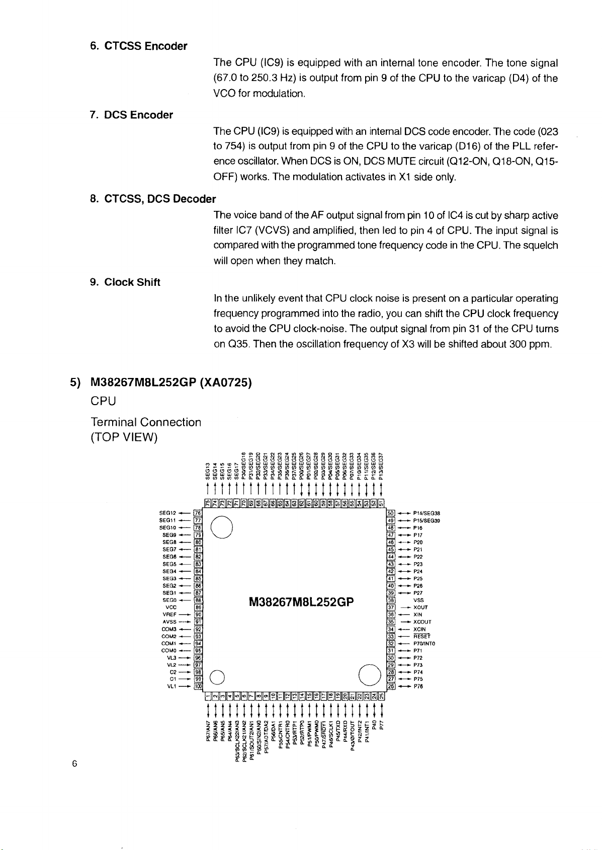
5) M38267M8L252GP (XA0725)
CPU
Terminal Connection
(TOP VIEW)
o3oio»-wn«fin<pseoaiO'-Nn’fV)iflN
O ’ri Ot CN liJ UJ UJ UJ UJ lU UJ lÜ LU UJ lll ll lUJ U JU JU JU JU JU Jl U
rr -r -r;ff l(n WM( /)Ml /)WW I/ )W WM W WW (0 1/ )»W
ulu il il iiJUAn Hr ir tAnnS pä äSöQ Orrrr
WWM lO« fl.Í La.ÍLa .IL ÍLÍL ¡L£ CLÍ £Q.£C LD.Íl.a(I.
o ü o o o c e J o o o o o o o o ü o o o o
mimtitttiimmmtt
SEG12
SEG11
SEG10
SEG9
SEG8
SEG7
SEG6
SEG5
SEG4
SEG3
SEG2
SEG1 @7
SEGO
VREF
AVSS
COM3
COM2
COMI
COMO
-----
--
-----
■*
-
------
-----
--
-----
-•
-----
—
-----
-
------
—
VCC m
-----
----
-•
-----
--
-----
-«
-----
--
-----
-----
►
VL3
--
_
VL2
-----
►
C2
C1
-----
► [99
VL1
— ►
m
m.
m
[TO
E
[H
[83
E
IM
[86
ÜB
[90
E
[92
m
E
El
[96
[97
¡9B
g ®
O
M38267M8L252GP
m-
0 -
46] -
¿u-
44) -
jg-
42]-
43-
40] -
34].
= '
H] ■*
m -
30) -
29 -
n
27) -
26) -
-
• P14/SEG38
• P15/SEG39
• P16
• p i ;
P20
• P21
- P22
- P23
- P24
• P25
• P26
• P27
VSS
- XOUT
XIN
• XCOUT
XCIN
RESET
P70/INTO
• P71
• P72
• P73
• P74
- P75
• P76
S S I
< < <
3 a 3
§ 2
< <
: I ö
ÚÚ
Si
Q. Q.
K ip
c Q s
lw $ y
£ § CL
Q h N
X £
f o ?
1 t
? Q y
II
cSt
5 CL Q.
6
Page 7
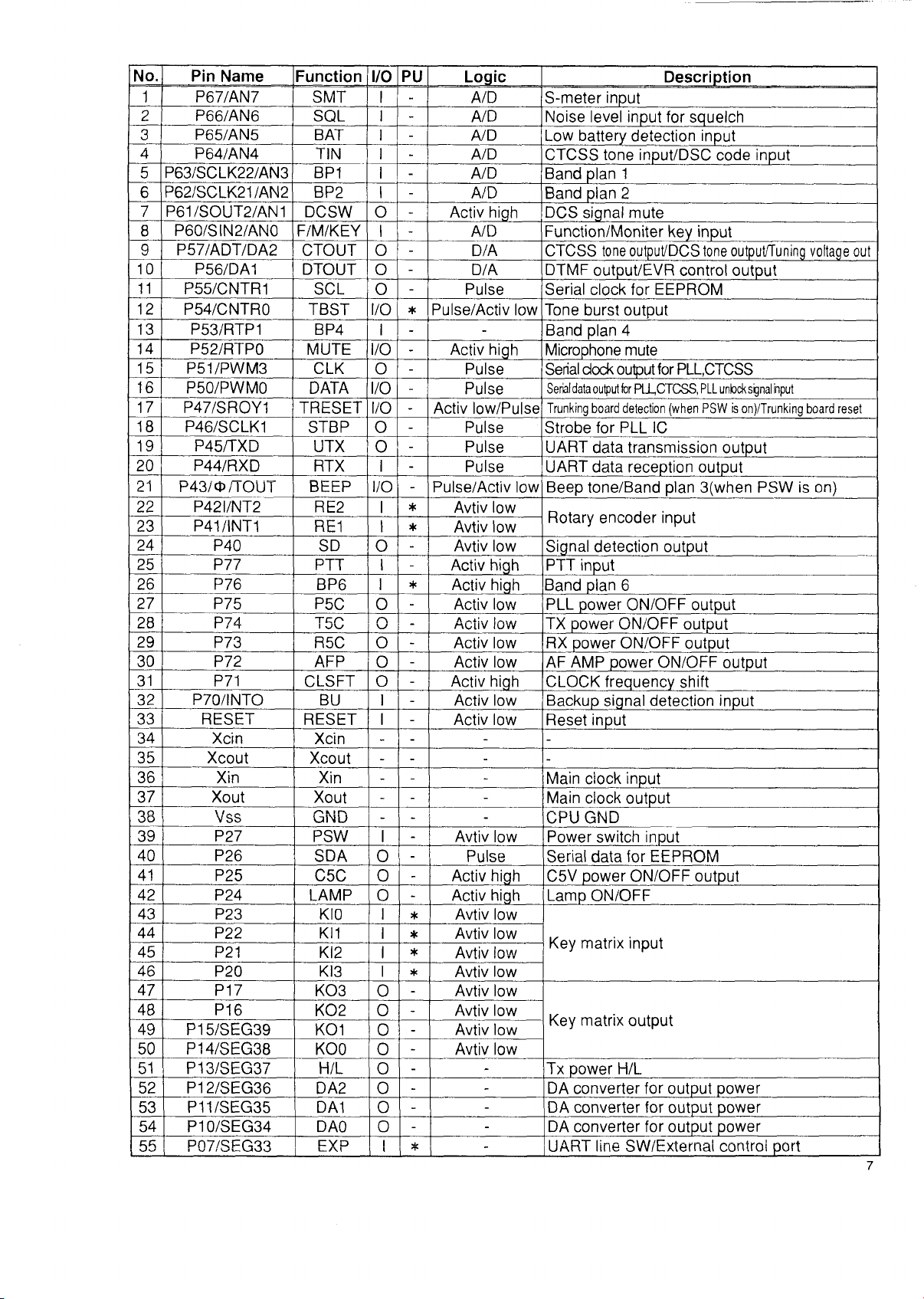
No.
1
2
3 P65/AN5
4 P64/AN4
5 P63/SCLK22/AN3
Pin Name
Function I/O PU Logic Description
P67/AN7 SMT
P66/AN6 SQL I
BAT I
TIN I
BP1
6 P62/SCLK21/AN2 BP2 I
7
P61/SOUT2/AN1 DCSW o
8 P60/SIN2/ANO
9 P57/ADT/DA2
10
11
12
P56/DA1
P55/CNTR1
P54/CNTR0 TBST I/O
13 P53/RTP1
14
15
16
17
18
P52/RTP0 MUTE
P51/PWM3 CLK
P50/PWM0 DATA
P47/SROY1 TRESET
P46/SCLK1 STBP
19 P45/TXD
20
21
P44/RXD RTX I
P43/0/TOUT
22 P42I/NT2
23 P41/INT1
24
25
P40 SD
P77
26 P76
27
28
29
30
P75
P74
P73
P72 AFP
31 P71
32
P70/INTO BU I
33 RESET
34
35
Xcin
Xcout
36 Xin
37
Xout
38 v'ss
39
40
41
P27
P26
P25
F/M/KEY I
CTOUT 0
DTOUT o
SCL
BP4 I
UTX
BEEP
RE2
RE1 I
PTT I
BP6
P5C 0
TCO
1 v^V-/
R5C o
CLSFT o
RESET I
Xcin
Xcout
Xin
Xout
GND
PSW I
SDA
C5C 0
42 P24 LAMP
43 P23
44
P22 KI1
45 P21
46 P20
47
P17
KI0
K!2
KI3
K03
48 P16 K02
49 P15/SEG39 KOI
50 P14/SEG38
KOO 0
51 P13/SEG37 H/L
52
P12/SEG36 DA2 0
53 P11/SEG35 DA1 0
54
55
P10/SEG34
P07/SEG33
DA0
d Y D
L .A I
-
I
-
-
-
-
I
-
-
-
-
-
-
0
*
- -
-
I/O
-
0
-
I/O
-
I/O
-
0
-
0
-
-
I/O
*
I
*
-
0
-
*
I
-
r\
-
-
-
0
-
-
-
- - - -
- - - -
- - -
- - -
- - -
-
-
0
-
-
0
A/D
A/D
A/D
A/D
A/D
A/D
Activ high
A/D
D/A
D/A
Pulse Serial clock for EEPROM
Pulse/Activ low
Activ high
Pulse Serial dock output for PLL,CTCSS
Pulse
Activ low/Pulse
Pulse
Pulse UART data transmission output
Pulse UART data reception output
Pulse/Activ low
Avtiv low
Avtiv low
Avtiv low
Activ high PTT input
Activ high
Activ low
a . i
____
AAUllV IUW
Activ low
Activ low
Activ high
Activ low
Activ low
Avtiv low
Pulse Serial data for EEPROM
Activ high C5V power ON/OFF output
Activ high
I * Avtiv low
*
I
!
I
0
0
0
0
0
Avtiv low
*
Avtiv low
*
Avtiv low
-
Avtiv low
-
Avtiv low
-
Avtiv low
-
Avtiv low
- -
- -
- -
- -
T“
-
S-meter input
Noise level input for squelch
Low battery detection input
CTGSS tone input/DSG code input
Band plan 1
Band plan 2
DCS signal mute
Function/Moniter key input
CTCSS tone output/DCS tone output/Tuning voltage out
DTMF output/EVR control output
Tone burst output
Band plan 4
Microphone mute
Serial data output lor PLLCTCSS, PLL unlock signal input
Trunking board detection (when PSW is on)/Trunking board reset
Strobe for PLL IC
Beep tone/Band plan 3(when PSW is on)
Rotary encoder input
Signal detection output
Band plan 6
PLL power ON/OFF output
TX power ON/OFF output
RX power ON/OFF output
AF AMP power ON/OFF output
CLOCK frequency shift
Backup signal detection input
Reset input
Main clock input
Main clock output
CPU GND
Power switch input
Lamp ON/OFF
Key matrix input
Key matrix output
Tx power H/L
DA converter for output power
DA converter for output power
DA converter for output power
UART line SW/External control port
7
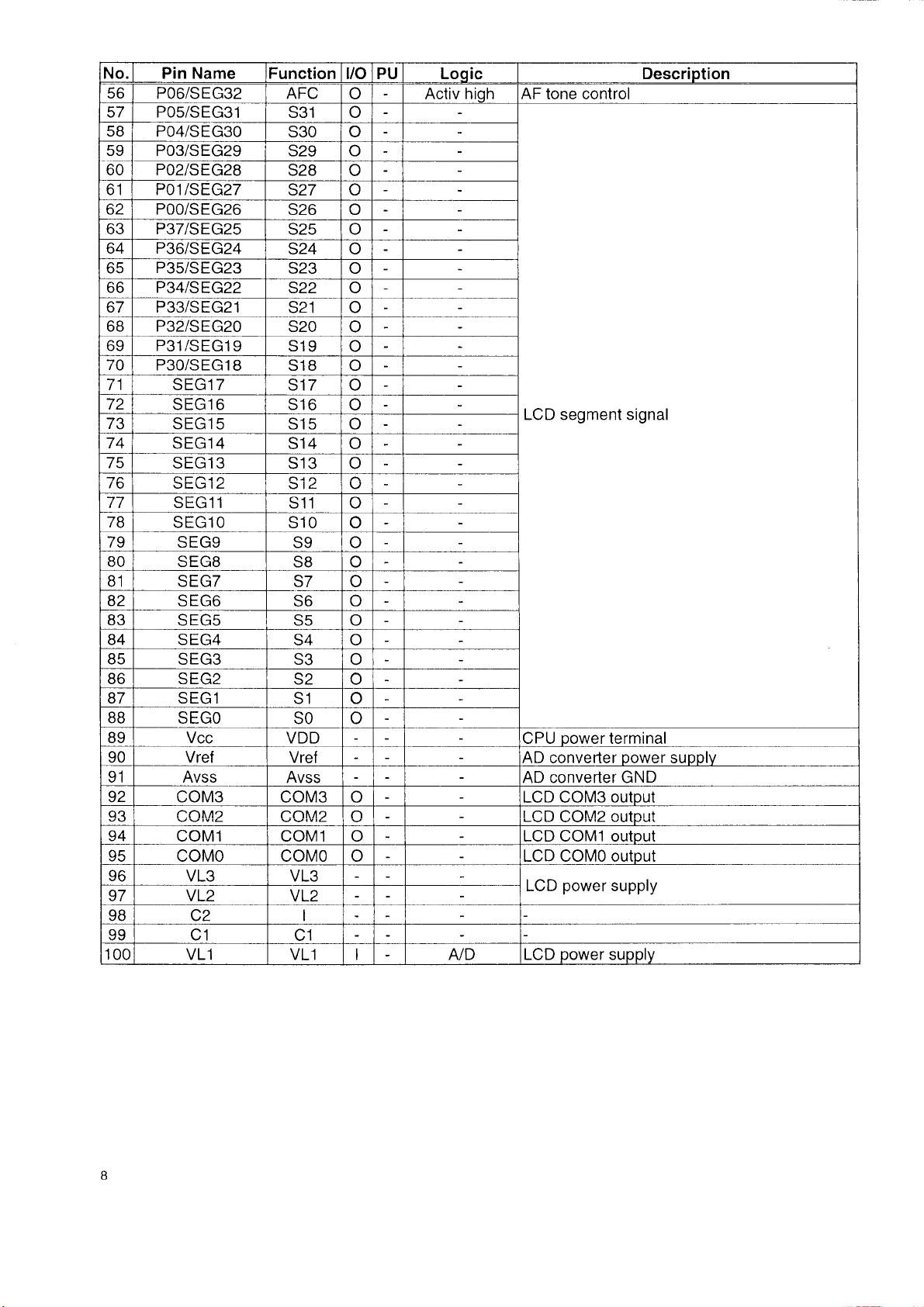
Page 8
No.
li e T
57 '
58 "
59 "
60
61
62 '
63
64 "
65 “
66 '
67 '
68 '
69 "
70 ‘
71
111
73 ~
74 "
75 ‘
-7/-'
( O
T T "
78 ~
79
80
81
82
83
84
85
86
87 '
88
89
90
91
92
93
~94~
95
96
97
98
99
100
Pin Name Function I/O PU Logic Description
P06/SEG32 AFC
P05/SEG31
P04/SEG30
P03/SEG29
P02/SEG28
P01/SEG27
P00/S EG26
P37/SEG25
P36/SEG24
P35/SEG23
P34/SEG22
P33/SEG21
P32/SEG20
P31/SEG19
P30/SEG18
SEG17
SEG16
SEG15
SEG14
SEG13
SEG11
SEG10
SEG9
SEG8
SEG7
SEG6
SEG5
SEG4
SEG3
SEG2
SEG1
SEGO
S31 O
S30 O
S29 O
S28
S27 O
S26 O
S25 O
S24 O
S23 O
S22 O
S21
S20
S19 O
S18 O
S17 O
S16 O
S15 O
S14 O
S13 O
S11 o
S10 o
S9 O
S8 O
S7 O
S6 O
S5 O
S4 O
S3 O
S2
S1 o
SO o
Vcc VDD
Vref
Avss
COM3
r n M Q
Vref AD converter power supply
Avss AD converter GND
COM3 O LCD COM3 output
nniwio
O Activ high AF tone control
O
O
LCD segment signal
O
CPU power terminal
n
LCD COM2 output
COM1 COM1 O LCD COM1 output
COMO COMO O LCD COMO output
VL3
VL2
VL3
VL2
LCD power supply
C2
C1
VL1
C1
VL1
A/D LCD power supply
Page 9
SEMICONDUCTOR DATA
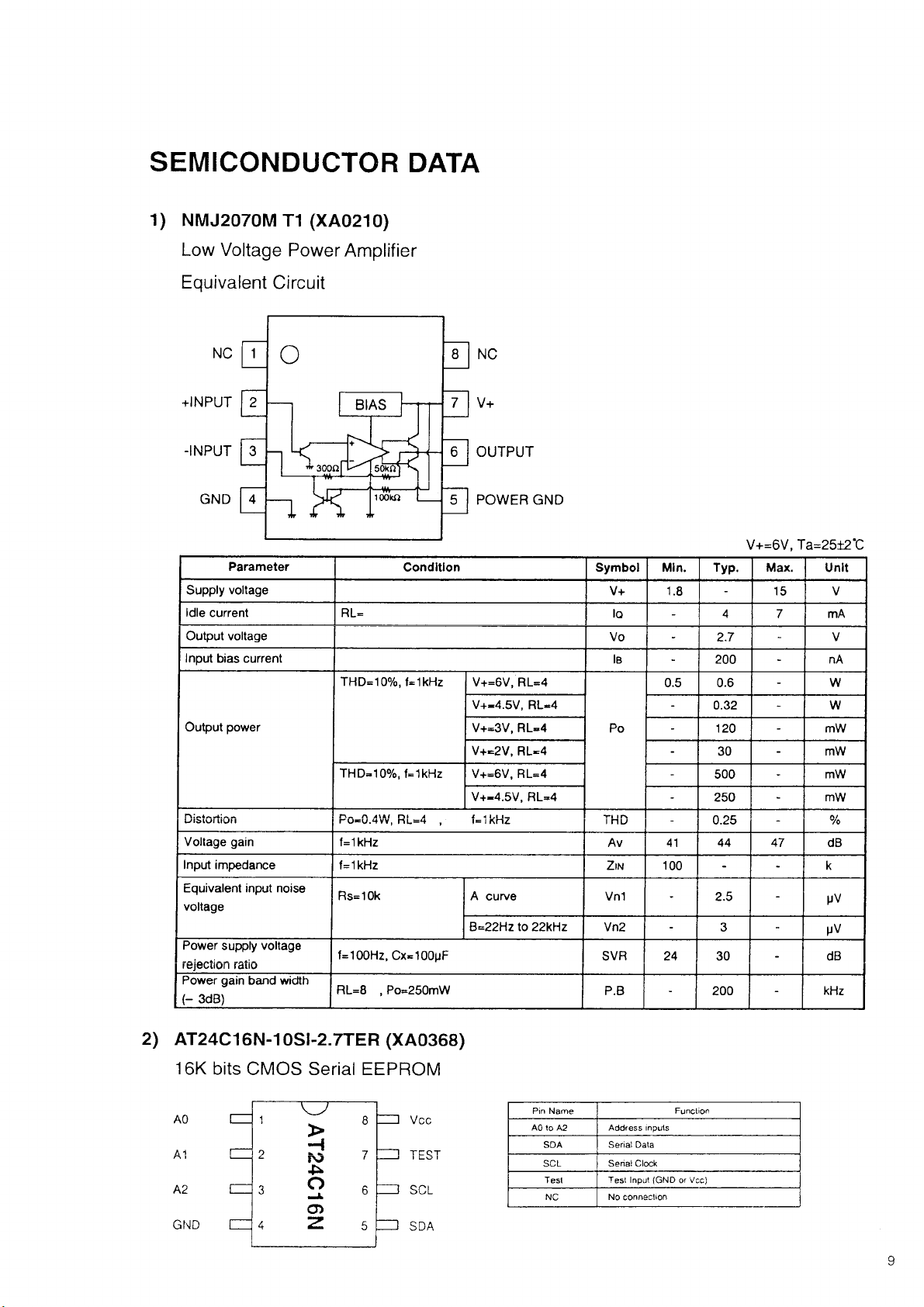
1) NMJ2070M T1 (XA0210)
Low Voltage Power Amplifier
Equivalent Circuit
Parameter
Supply voltage
Idle current
Output voltage
Input bias current
Output power
UldllM IIUI1
Voltage gain
Input impedance f=1kHz
Equivalent input noise
voltage
Power supply voltage
rejection ratio
Power gain band width
(- 3dB)
RL=
THD=10%, f= 1 kHz
THD=10%, f=1kHz V+=6V, RL=4
f-v_ r\ A\ki i a i 4 i-i i_
ru*u.^vY, n L ^ , i= i
f=1kHz
Rs=10k
f= 100Hz, Cx»100pF
RL=8 , Po=250mW
Condition
Symbol
V+
Vo
V+=6V, RL=4
V+-4.5V, RL-4
V+=3V, R L-4
V+=2V, RU 4
V+-4.5V , RL=4
A curve Vn1
B=22Hz to 22kHz
Po
Tnu
Av 41 44 47 dB
ZlN
Vn2
SVR
P.B
V+=6 V, Ta=25±2‘C
Min. Typ. Max.
1.8
lo
-
-
Ib
-
0.5 0.6
-
-
-
-
-
-
100
-
-
24 30
'
-
4 7 mA
2.7
200
0.32
120
30
500
250
0.25
- -
2.5
3
200
15
-
-
-
-
-
-
-
-
-
-
-
-
-
Unit
V
V
nA
W
W
mW
mW
mW
mW
%
k
MV
MV
dB
kHz
2) AT24C16N-10SI-2.7TER (XA0368)
16K bits CMOS Serial EEPROM
AO
A 1
A2
GND
Pin Name
A0 10 A2 Address inputs
SDA Serial Data
SCL Serial Clock
Test Test Input (GND or Vcc)
NC
No connection
Function
9
Page 10
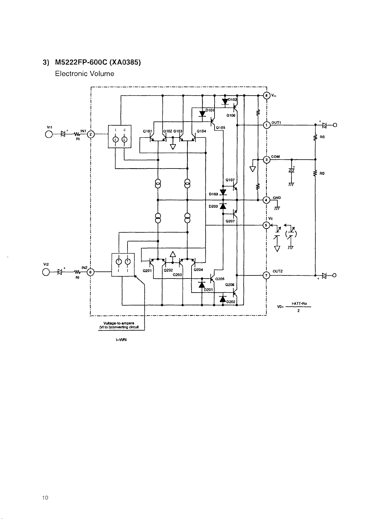
3) M5222FP-600C (XA0385)
Electronic Volume
VI1 I
VI2
O —
----
VW—(e>
fc -0
7 ^ - °
10
l=WHI
Page 11
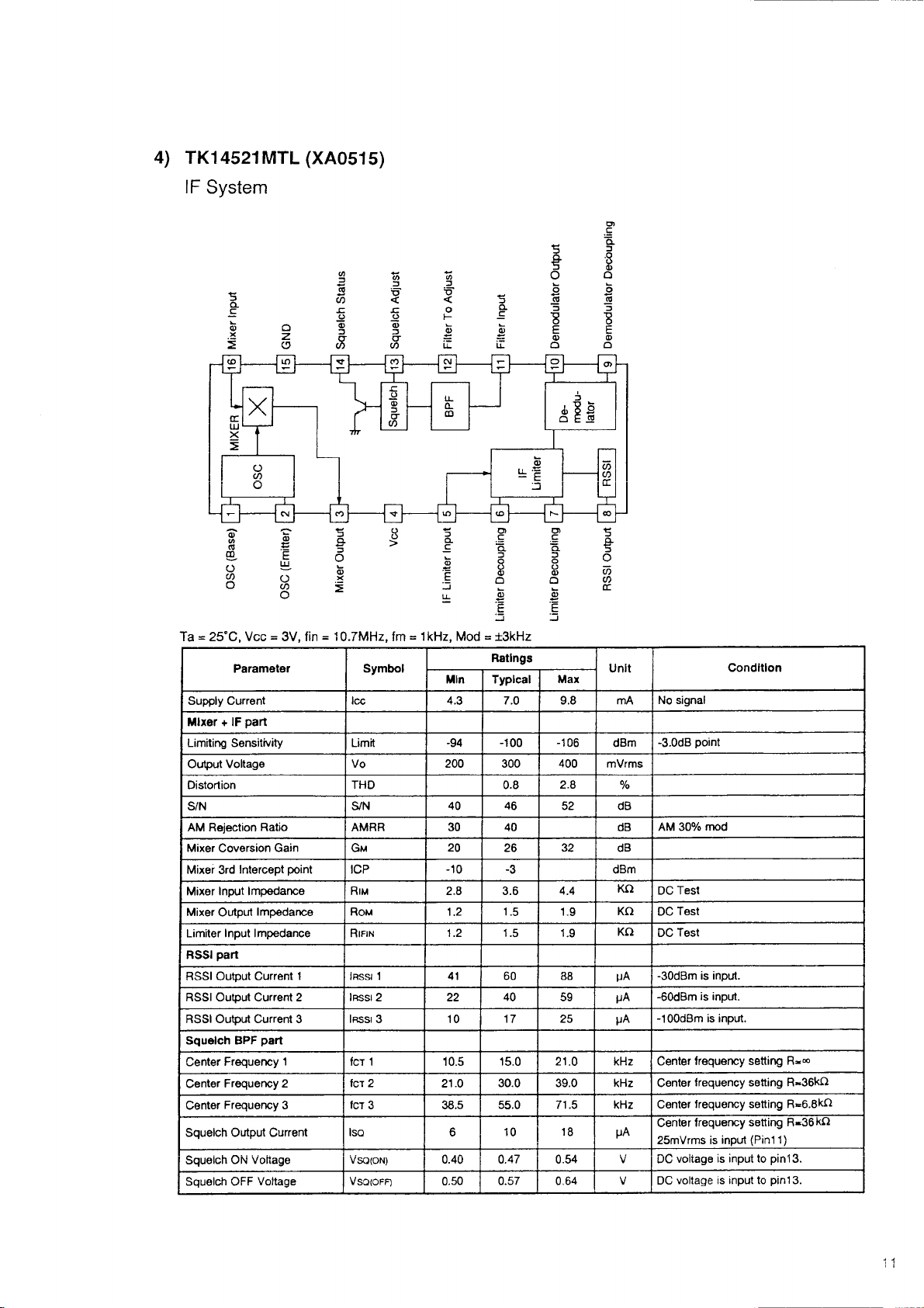
4) TK14521MTL (XA0515)
IF System
c
H
3
Q.
Û
z
0
w
m
O
co
O
Ta = 25°C, Vcc = 3V, fin = 10.7MHz, fm = 1kHz, Mod = ±3kHz
Parameter Symbol
Supply Current Icc 4.3 7.0
Mixer + IF part
Limiting Sensitivity
Output Voltage Vo
Distortion THD 0.8
S/N
AM Rejection Ratio
Mixer Coversion Gain Gm 20 26 32
Mixer 3rd Intercept point ICP -10 -3
Mixer Input Impedance Rim 2.8 3.6 4.4
Mixer Output Impedance
Limiter Input Impedance
RSSI part
RSSI Output Current 1 Irssi 1 41 60 88
RSSI Output Current 2
RSSI Output Current 3 Irssi 3 10 17 25
Squelch BPF part
Center Frequency 1 fCT 1 10.5 15.0 21.0
Center Frequency 2 fCT 2 21.0 30.0
Center Frequency 3 fCT 3 38.5 55.0
Squelch Output Current Iso 6 10
Squelch ON Voltage VSQ(ON) 0.40
Squelch OFF Voltage
ç
E
W
O
CO
O
¿5
co
$
Ô
x>
<
s
B
>
Limit
S/N 40 46 52 dB
AMRR 30 40 dB
Rom 1.2
Rifin 1.2
I RSSI 2 22 40 59
VSQ(OFF) 0.50 0.57
'O
<
o
Ratings
Min Typical
-94
200 300 400 mVrms
-100 -106
1.5 1.9
1.5 1.9
0.47
?
a
o
ra
Z)
E
0)
Max
2.8
39.0 kHz
71.5 kHz
0.54 V
0.64 V
o
«
E
E
0
Q
t
o
to
co
DC
Unit
9.8 mA
dBm
dBm
kHz
18
Condition
No signal
-3.0dB point
%
AM 30% mod
dB
Kn
DC Test
Kn DC Test
Kn
DC Test
-30dBm is input.
ma
-60dBm is input.
(JA
-100dBm is input.
ma
Center frequency setting R-«
Center frequency setting R*36kO
Center frequency setting R=6.8kn
Center frequency setting R«36kn
ma
25mVrms is input (Pin11)
DC voiiage is input to pinl 3.
DC voltage is input to pinl 3.
Page 12
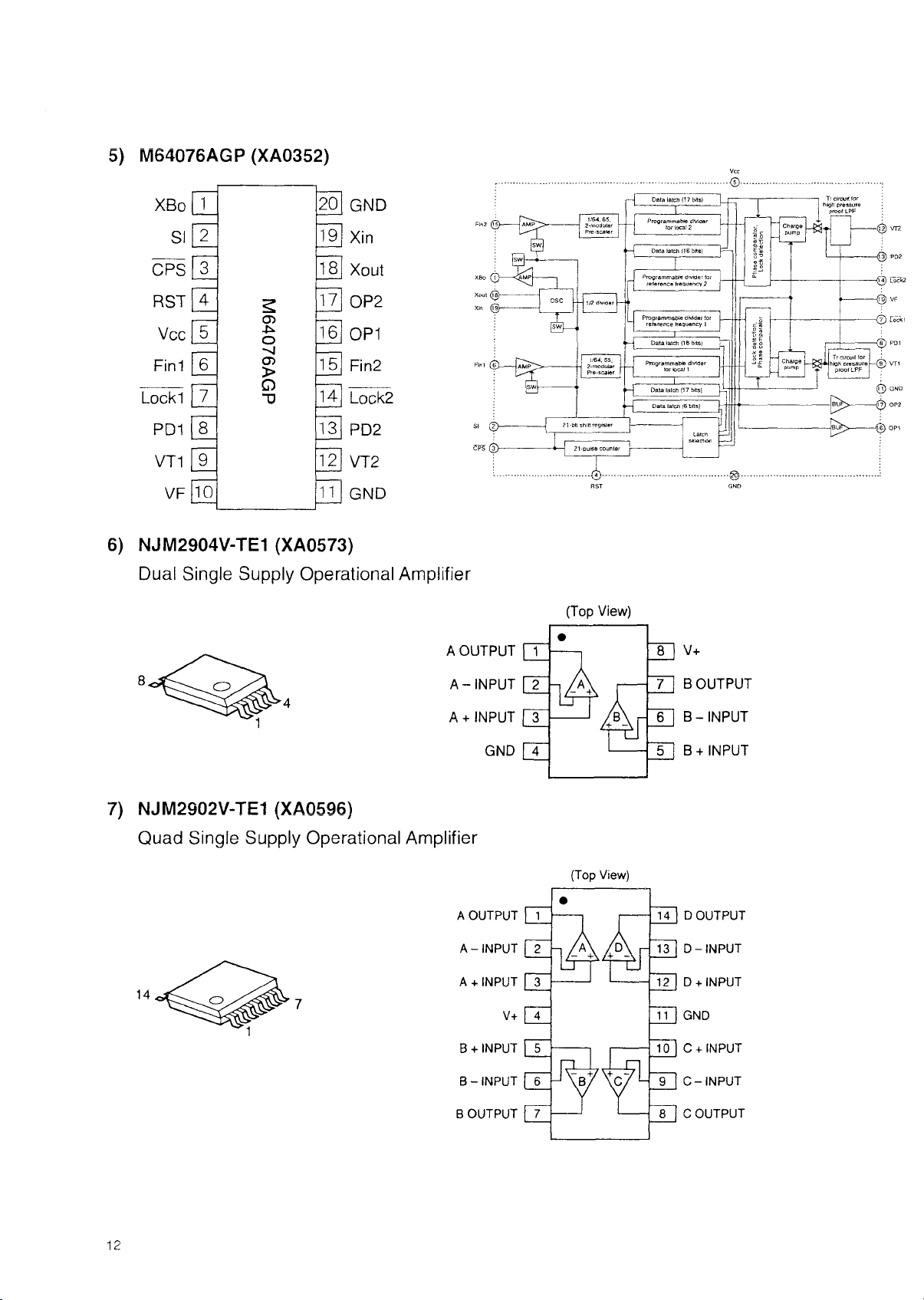
5) M64076AGP (XA0352)
XBo
SI
CPS
RST
1 20
2
3 18
4 17
19
GND
Xin
Xout
OP2
a>
Vcc
Fin 1
Lockl
PD1
VT1
VF [10
b
6
7
o
-nI
O)
>
O
U
8 13
9
16
15
14
12
11
OP1
Fin2
Lock2
PD2
VT2
GND
6) NJM2904V-TE1 (XA0573)
Dual Single Supply Operational Amplifier
(Top View)
7) NJM2902V-TE1 (XA0596)
Quad Single Supply Operational Amplifier
A OUTPUT Q
A -IN P U T [ j T
A + INPUT [ T
GND ¡ ~ r
(Top View)
A OUTPUT Q _
A -IN P U T f | 7 -
L ir
A + INPUT [ T
v+ [jT
B +INPUT [~5~-
B - INPUT | 6 [- 1 \ B / \ C
J J V+
~7~[ B OUTPUT
(T ] B -IN P U T
5 l B + IN P U T
14 DOUTPUT
13 I D -INP U T
12 D t INPUT
11 GND
10 C +INP UT
9 C-IN PU T
12
B OUTPUT f T
8 C OUTPUT
Page 13

8) S-81350HG-KD-T1 (XA0724)
Top View
I \
1 VOUT
2 GND
3 Vin
m z r u
9) S-80845ALMP-EA9-T2 (XA0620)
Voltage Regulator
Vin=18V
lout= 100mA
NC NC
E A 9 *
GND V in V out
10) 2SK2975 OCE0038)
Drain
Source
Gate
* Lot number
Maximum ratings
Ratings
Drain-Source Voltage
Total Device Dissipation @Tc=20°C Pd
Gate-Source Voltage Vgss
Storage Temperature Range Tstg
Operating Junction Temperature
Characteristic
Ratings
Drain-Source Breakdown Votage
Vds=17, Vgs=0V Idss
Zero Gate Voltage Drain Current
Vgs=10, Vds=0V Igss
Gate Threshold Voltage Vds^.ô,
Ids—1 mA
Out Put Power
f^450MHz Pin=1W Vds=9.6V Po 7.0
Drain Efficiency
f=450MHz Pin=1W Vds=9.7V
Symbol
Vdss
Tj
Symbol
Vth
V
D
Value
30
10
±20
I
X
0
175
Min
,
_
1.0
50
Unit
V
W
+
Max Unit
10
1 uA
1.7
_
_
V
1
°c
°C
uA
V
W
%
Page 14

11) Transistor, Diode, and LED Ontline Drawings
Top View
1 o\
LCD Connection
' <-)
O v-< ^ l O C O r— CO CT5 »-i ‘ ^ ' <—‘ * — ' *—1 1 T_ ' CQ C\2 0 0 D O D O DO 00 DJ C\J C\S CO CO
{/3COC/)t/}WCOCOC/}COt/}COCOCOC/}C/2COCO&Q(/)COt/)C/]C/2C/3C/}£OCOC/2C/)C/3C/}C/3
14
/ C i r \ n a a \
^ L L U U 4 4 j
o ^ c\i co tj* id <x> r- co en o T-t oo n -c io co r*- cd cn © ^
SEGMENT
COMMON
Page 15

EXPLODED VIEW
1) Front View
I KZ0108(DJ-493)
\ KZ0098(DJ-496)
DJ-493 only
15
Page 16

2) Rear View
ST0063
16
Page 17

PARTS LIST (DJ-493)
DJ-493 Main Unit
Ref No.
C1
C2
C3
C4
C5
C6
C l
C8
C9 CU3005
C10 CU3009
C 11
C12
C13
C14
C 15
Cl 6 CU3031
C17
C18
C19 CU3035
C20
C21
C22 NC
C23
C24
C25
C26
C27
C28
C29 NC
C30
C31
C32
C33
C34
C35
C36 CU3031
C37
C38
pon
I/O C?
C40
C41
C42
C43
C44
C45
C46
C47
C48
C49
r in
C51
C52 NC
C53
C54
Parts No.
CU3031
CU3031 C 1608J B 1H 471K T -A S
CU3057
CU3014
CU3031
CU3031
CU3007
CU3031
r>i nnna
VJUÜUUi/
CU3001
CU3031
CU3001
CU3031
CS0408 6MCM 156M ATER
CU3007 C1608CH1 H 060CT-A
CU3014 C1 608CH1 H 180JT-A S
CU3011
CU3001
CU3012 C1 608CH1 H 120JT-A S
CU3031
CU3031
CU3009
CU3001
CU3012
CU3006
CU3002
CU3031
CU3047
CU3031
CU3017
CU3001
NC
CU3011
CU3031
CU3031
CU3023
CU3031
CU3031
CU3031
CU0108
CU3031
CU3013
u r
NC
CU3031
CU3047
Parts Name
DJ-493 Main U n it
C1608JB 1 H 4 71KT-AS
C1608C H 1H130JT-A
C1608CH1H180 JT-AS
C1608JB 1H471KT-AS
C1608JB 1H471KT-AS
C1608CH 1H060CT-A
C1608JB 1H471KT-AS
C1608C H 1H040CT-AS
C1608C H 1H080CT-A
Cl 608CH1H080C T-A
C1608CH1H0R5CT-AS
C1608JB1H471KT-AS
C1608CH1H0R5CT-AS
C1608JB1H471 K T-AS
C1608JB 1 H 4 71KT-AS
C1608JB 1H102 K T -AS
C160 8CH 1H100DT-AS
C1608CH1H0R5CT-AS
C1608 JB1H471 K T -A S
C1608JB1H471 K T-AS
C160 8CH1H080CT-A
C1608CH1H0R5CT-AS
C1608C H 1H120JT-AS
C1608C H 1H 050CT-A S
C1608CH1H010CT-AS
C1608JB1H471 KT-AS
C1608JB1H103KT-N
C1608JB1H471 KT-AS
C1608JB1H471 KT-AS
C1608C H1H330JT-AS
C1608CH 1H0R5CT-AS
C1608CH1 HI 00D T-A S
C1608JB1H471 KT-AS
C1608JB1H471 KT-AS
C1608CH1H 101JT-AS
C1608JB1H471 KT-AS
C1608JB1H471 K T-AS
C1608JB1H471 KT-AS
LMK212BJ105KG
C1608JB1H471 KT-AS
C1608CH1H150 JT -AS
Cl 608JB1H471 KT -AS
C1608JB1H103KT-N
Ver.
Ref No. Parts No.
DJ-493 Main U nit
C55
C56
C57
C58 CU3009 C1608C H 1H080CT-A
C59 CU3015 C1608CH1H220JT-AS
C60
C61 CU3005
C62
C63
C64 CU3047 C1608JB 1H103KT-N
C65
C66 CU3004
C67
C68 CU3023 C1608CH1H10 1JT-AS
C69 CU3047
C70 CS0407
C71 CU3001 C1608CH1H0R5C T-AS
C72 CU3035 C1608JB 1H 102KT-A S
C73
C74 CU3031 C1608JB1H471 KT-A S
C75 CU3057 C 1608CH1H130JT-A
C76 CU3015 C1608CH 1H220JT-AS
C77
C78
C79 CU3002 C1608CH1H010C T-AS
C80
C81 CU3011
C82
C83 CU3031 C1608JB1H471 KT-A S
C84 CU3031
C85 CU0108
C86 CU3016 C 1608CH1H270JT-A S
C87 CU3035 C1608JB 1H 102KT-A S
C88 CS0213
C89 CU3016 C1608CH1H270JT-A S
C90
C91 CU3035 C 1608JB1H102KT-AS
C92
C93
C94
C95 CS0408
C96 CU3111 C 1608JB1C104K T-N
C97
C98
C99
C100
C101 CU3047 C1608JB 1H 103KT-N
C102 CU3035 C1608JB1H 102KT-AS
C103 CU0108
C l 04 CU3035 C 1608JB1H 102KT-AS
C105 CS0404
C106 CU3015 C1 608CH1H220JT-AS
C107 CS0408
C108 CU3035
CS0408
CU3015
CU3004 C1608CH1H030CT-A S
CU3012
CU3006
NC
CU3004
CU3006
CU3Q47
CU3012 C1608CH 1H120JT -A S
CU3014
CS0213
CU0108
CU0108
CU3035
CE0392
CU3035 C1608JB 1H 102KT-A S
CU0108
CU3047
CS0408
CS0408
6MCM 156MATER
C1608C H 1H220JT-AS
C1608CH1H120JT -A S
C1608CH1H040CT-AS
C1608CH1H050CT-AS
Cl 608C H 1H030CT-AS
C1608CH1H030C T-AS
C1608CH1H050CT-AS
C1608JB1H103KT-N
35MC104MATER
C1608JB1H103KT-N
C1608C H 1H 180JT-AS
TMCMA1A225MTR
C1608CH 1H100DT-A S
LMK212BJ105KG
C1608JB1H471 K T -A S
LMK212BJ105KG
TMCMA1A225M TR
LMK212BJ105KG
C1608JB1H 102KT-AS
6MV47UW
6M CM156MATER
LMK212BJ105KG
C1608JB1H103K T -N
6MCM156MATER
6MCM156MATER
LMK212BJ105KG
6MCM106MATER
6MCM 156MATER
C1608JB1H102KT-AS
Parts Name
Ver.
17
Page 18

DJ-493 Main Unit
Ref No.
Parts No.
Parts Name
DJ-493 Main Unit
C109
C110
c m
C112
C l 13
C114
C115
C 116
C117
C l 18
C l 19
C120 CU3035
CE0350 16MV100HC
CU3035
CE0397
C1608JB1H 102KT-AS
MVS16VC47M F46
CU0108 LMK212BJ105KG
CU3047 C1608JB1H103KT-N
CU3035 C1608JB 1H 102KT-AS
CE0392 6MV47UW
CU3111 C 160 8JB1C104K T -N
CU3047 C1608JB1H103KT-N
CS0408
6MCM156MATER
CU3047 C l 608JB1 H I03K T -N
C1608JB 1H 102KT-AS
C121 CS0408 6MCM156MATER
C122
C123
C124
CU3111
CU3111 C 1 608JB1C104KT-N
CU3035 C1608JB 1H 102KT-AS
C125 CU3051
C126
C127
C128
CU3051 C1 608JB1E22 3KT-NS
CU3051 C 1608JB 1E 223KT-N S
CU3111
C 129 CU3111
C130
C 131
C132
C133
CU0108 LMK212BJ105KG
CU3111
CE0396
CS0408
C134 CU3111
C135 CU3035
C136
C137
CU3035 C1608JB 1H 102KT-A S
CU3101
C138 CU3111
C139
C140
CU0108 LMK212BJ105KG
CU3035
C141 CU3035
C142
C143
C144
C145
C l 46
n 1 a ~i
Vj I /
CU3047
CU3035
CU3111
CU3025
CU3035
r'l nm c;
u u u u u v ;
C148 CU3111
C149
C150
C 151
CU3041
CU3111
CU3111
C152 CU3035
C153
CU3035
C154 CU3038
C155
C156
C157
CU3111
CU3035
CU3050
C l 58 CUQ1Q8
C 159
C160
C 161
C162
CU3051
CU0108
CS0408
CU3023
C1608JB 1C 104KT-N
C1608JB1E223K T -NS
C1608JB 1C 104KT-N
C1608JB 1C 104KT-N
C1608JB1C104KT-N
MVS6.3VC100MF46
6MCM156MATER
C1608JB 1C104KT-N
C1608JB1H102KT-A S
C1608JB 1C473KT-N S
C1608JB1C104KT-N
C1608JB1H102KT-A S
C1608JB1H102KT-A S
C1608JB1H103KT-N
C1608JB 1H102KT-A S
C1608JB1C104KT-N
C1608CH1H151JT-AS
C1608JB1H 102KT-AS
riR n o ir 1 u 1 nok'T— a q
W i i i i i \ i r~wj
C1608JB1C104KT-N
C1608JB1H332KT-NS
C1608JB1C 104KT-N
C1608JB 1C104KT-N
C1608JB 1H102K T -AS
C1608JB 1H 102KT-A S
C1608JB 1H 182KT-A S
C1608JB 1C104KT-N
C1608JB 1H 102KT-AS
C1608JB1E183K T-NS
LMK212BJ105KG
C1608JB 1E223KT-NS
LMK212BJ105KG
6MCM156MATER
C1608CH1H101JT-AS
Ver.
Ref No. Parts No. Parts Name
DJ-493 Main Unit
C163
C 164
C165
C166 CU3047
C167
C 168
C169
CU3044 C 160 8JB1H562KT-NS
CU3040 C 160 8JB1H272K T-NS
CU3111
C1608JB 1C 104KT-N
C1608JB1H103KT-N
CU3101
C1608JB1C473KT-N S
CU3047 C 1608J B 1H 103KT-N
CU3047 C 1 608JB1H103 K T -N
C170 CU3047 C 160 8JB1H103K T -N
C171
CU3046 C 1608JB1H822KT-NS
C172 CU3035 C 1608JB 1H 102KT-AS
Cl 73
CUQ108 LMK.212BJ105KG
C174 CS0408 6MCM1 56MATER
C175 CU3111
C1608JB 1C 104KT-N
C176 CU3014 C1608CH1H180JT-AS
C177 CU3013 C1608C H 1H 150 JT-AS
C178 CU0108
C179 CU3035
LMK212BJ105KG
C1608JB1H 102KT-AS
C180 CU3111 C 1608JB1C 104K T -N
C 181 CU3049 C1608JB1E153K T -NS
C182 CU3031 C1608JB 1H 471KT-AS
C183
CU3031 C 1608J B 1H471K T-A S
C184 NC
C185 CU3111
C186
CU3003 C1 608CH1 H 0 20CT-AS
C 187 CU3111
C1608 JB1C104KT-N
C1608 JB1C104KT-N
CN1 NC
CN2 NC
CN3 NC
D1 XD0323 MA2S111-TX
D2
D3
D4 XD0331
D5
D7 XD0251
D8
D9 XD0323
D10
D11
n i o
i_y i
D13 XD0344
XD0326 1 SV307(TPH3)
XD0344 1SV311 (TPL3)
HSU277TRF
XD0331 H SU277TRF
MA741W A TX
XD0261 S3DG7
MA2S111-T X
XD0130 DA204U T 106
XD0294 U2FWJ44NCTE12R)
Y n m /i/i
/ \ L-/ 1SV311 (TPL3)
1SV311 (TPL3)
D14 XD0344 1SV311 (TPL3)
D15
D16 XD0131
XD0344
1SV311 (TPL3)
1SV214 TPH4
D17 XL0036 SM L-31OMTT86
D18
D19 XL0028
XL0036 S M L-310M TT86
BRPG1201W TR
D20 NC
D21 NC
D22 NC
D23 NC
D24 NC
D25
D26
XD0332
XD0291
D27 XD0342
RB706F-40-T106
MA729-T X
1SS390 TE61
Ver.
18
Page 19

DJ-493 Main Unit
Ref No.
Parts No. Parts Name Ver.
DJ-493 Main Unit
FL1
XC0072 ALFCM 455F=K
IC1 XA0449 UPC2710T-E3
IC2 XA0352
IC3 XA0724
M64076GP
S81350HG-K D -T1
IC4 XA0515 TK14521M TL
IC5 XA0210
IC 6
IC7
IC8
IC9
IC I 0
IC 11
JK1
JK2
JK3
XA0385 M 5222FP-600C
XA0596 NJM 2902V-TE 1
XA0573 NJM2904V-TE1
XA0725 M38267M8L252GP
XA0368 AT24C16N-10SI-2.7TE R
XA0620 S -80845ALM P-EA9-T2
UJ0046 MJ82-1
UJ0019 H S J1493-01-010
UJ0022 H S J1 1 0 2-01-5 4 0
L1 QC0507
L2 Q KA45A
L3
L4
QKA45A MR1.5 4.5T 0.4
QCQ5Q7 LK16081ROK-T
L5 QKA25A
L6
QKA25A MR1.5 2.5T 0.4
L7 QC0558
NJM2070M T 1
LK16081R0K-T
MR1.5 4.5T 0.4
MR1.5 2.5T 0.4
LL1608-FH5N6S
L8 QC0529 LQN21A18NJ04
L9 Q KA75A QKA75A
L10
L1 1
L12 QS40124
QC0573 LL1608-FHR1OJ
QC0565 LL1608-FH 22NJ
0.4-1.2 -4 T -L
L13 QC0567 LL1608-FH33NJ
L14
QC0561 LL1608-FH1ONJ
L15 QC0507 LK16081 ROK-T
L18 QC0507 LK16081 ROK-T
L19
L20
L21
L22
L23
L24
QC0561 LL1608-FH10N J
QC0528 LQN21A15NJ04
QC0528 LQN21A15NJ04
QC0564 LL1608-FH18NJ
QC0562 LL1608-FH 12NJ
QC0569 LL1608-FH47NJ
L25 QC0534 LQN21A 47NJ04
L26
L27
LCD1 EL0044
MIC1 EY0017
Q1
Q2
Q3
Q4 XE0034
Q5
Q6
Q7 XT0170
Q8 XT0172
Q9
Q10
Q11 XT0171
Q12 XU0193
QC0089 NL32252 2T -181JA
QC0507
LK16081 ROK-T
HT-3404
OB-27P44
XT0135 2SD2216R-TX
XE0038 2SK2975-T11-A
XT0138 2SC5066-0 (TE85L)
MRF9745T1
XT0138 2S C 5066-0(TE85L )
XU0172 XP1501-TX
2SB766A-TX
2SC 4618TLP
XT0138
2SC5066-0(TE85L)
XT0171 2SC4808-TX.AR
2SC4808-TX.AR
RN1107 TE85L
Ref No. Parts No.
Parts Name Ver.
DJ-493 Main U nit
Q13 XT0170 2SB766A-TX
Q14 XT0170 2SB766A-TX
Q15 XU0193 RN1107 TE85L
Q16 XU0172 XP1501-TX
Q1 7 XT0110 2SA1036K T146Q
Q18
Q19
Q20 XU0172
Q21 XU0161
XU0193 RN1107 TE85L
XU0197
RN1111 (TE85L)
XP1501-TX
XP1114(TX)
Q22 XU0192 RN2107 TE85L
Q23
XT0135 2SD2216R-TX
Q24 NC
Q25 NC
Q26
Q27
XU0193 RN1107 TE85L
XT0095 2SC4081 T106R
Q28 XU0192 RN2107 TE85L
Q29 XU0192 RN2107 TE85L
Q30 XU0195
m i
VJi 1 XT0135
RN1104 TE85L
2SD2216R-TX
Q32 XE0029 2SK1580-T1
Q33 XT0135
Q34 XE0029
Q35 XU0194
Q36 XU0197
2SD2216R-TX
2SK 1580-T1
RN2111 TE85L
RN1111 (TE85L)
Q37 XT0171 2SC 4808-TX.A R
R1
RK3030 MCR03EZHJ221
R2 RK3034 MCR03EZHJ471
R3 RK3046 MCR03EZHJ472
R4 RK3050 MCR03EZHJ103
R5
R6
RK3030
RK3066
MCR03EZHJ221
MCR03EZHJ224
R7 RK3014 MCR03EZHJ100
R8
RK3048
R9 RK3026
MCR03EZH J682
MCR03EZHJ101
R10 RK3018 MCR03EZHJ220
R11 RK3050 MCR03EZHJ103
R12 RK3063 MCR03EZHJ124
R13 RK3034
R14
RK3026
MCR03EZHJ471
MCR03EZHJ101
R16 RK3062 MCR03EZHJ104
R18 RK3050 MCR03EZHJ103
R19 RK3058 MCR03EZHJ473
R20 RK3062 MCR03EZHJ104
R21 RK3053 MCR03EZ HJ183
R22
R23
RK3056 MCR03EZHJ333
RK3052
MCR03EZ HJ153
R24 RK3058 MCR03EZHJ473
R25 RK0002 ERJ6GEYJ120V
R26 RK3050 MCR03EZHJ103
R27 RK3034
MCR03EZHJ471
R28 RK3042 MCR03EZHJ222
R29 RK3050 MCR03EZHJ103
R30
NC
R31 RK3026 MCR03EZHJ101
19
Page 20

DJ-493 Main Unit
Ref No. Parts No.
Parts Name Ver.
DJ-493 Main Unit
R33
RK3050
MCR03EZHJ103
R34 RK3062 MCR03EZHJ104
R35
RK3034
MCR03EZHJ471
R36 RK3066 MCR03EZHJ224
R37
R38 RK3046
R39 RK3062
R40
R41 RK3035
R42 RK3038
R43
R44
R45
R46 RK3032
R47 RK3030
R48
R49 RK3058
RK3050
RK3063
RK3050
RK3048
RK3050
RK3050
MCR03EZHJ103
MCR03EZHJ472
MCR03EZHJ104
MCR03EZHJ124
MCR03EZHJ561
MCR03EZHJ102
MGRQ3EZHJ103
MCR03EZH J682
MCR03EZHJ103
MCR03EZHJ331
MCR03EZHJ221
MCR03EZHJ103
MCR03EZHJ473
R50 RK3038 MCR03EZHJ102
R51 RK3026 MCR03EZHJ101
R52
RK3074
MCR03EZHJ105
R53 RK3074 MCR03EZHJ105
R54 RK3074
R55
R57
R58
R59
R60
R61
RK3074 MCR03EZH J105
RK3030 MCR03EZHJ221
RK3074
RK3066
RK3064
RK3050
R62 RK3058
R63
R64
R65
R66
R67
R68
R69
RK3062
RK3050
RK3058
RK3054
RK3076
RK3076
RK3058
R70 RK3054
R71 RK3042 MCR03EZHJ222
D “70
r w ¿
D u ' o n c o
[\ I\ JU J U
R73 RK3036
R74
RK3050
MCR03EZHJ105
MCR03EZHJ105
MCR03EZH J224
MCR03EZHJ154
MCR03EZHJ103
MCR03EZHJ473
MCR03EZH J104
MCR03EZHJ103
MCR03EZHJ473
MCR03EZHJ223
MCR03EZHJ155
MCR03EZH J155
MCR03EZHJ473
MCR03EZHJ223
y r i D n o c 7 u
IVIWPvUOl_Z_l 10 ^ / 0
\A~tn
MCR03EZHJ681
MCR03EZHJ103
R75 RK3058 M CR03EZHJ473
R76 RK3054
R77
RK3050
MCR03EZHJ223
MCR03EZHJ103
R78 RK3054 MCR03EZHJ223
R79
R80 RK3062
R81
RK3022
RK3042
MCR03EZHJ470
MCR03EZH J104
MCR03EZHJ222
R82 RK3046 MCR03EZHJ472
R83 RK305Q
m v i
_
£_i I i
\j
Mr.RmP7i-i. u rn
R84 RK3036 MCR03EZHJ681
R85
R8 6
R87
RK3050
MCR03EZHJ103
RK3038 MCR03EZHJ102
RK3050 MCR03EZHJ103
Ref No. Parts No. Parts Name Ver.
DJ-493 Main Unit
R88 NC
R89
R90
RK3001 M CR03EZHJ000
RK3032 MCR03EZHJ331
R91 RK3062 MCR03EZHJ104
R92 RK3058 MCR03EZHJ473
R93
R94 RK3050
R95
RK3050
NC
MCR03EZHJ103
MCR03EZHJ103
R96 RK3032 MCR03EZHJ331
R97 RK3058 MCR03EZHJ473
P Q Q
1 VJ RK3044
M n o m p y N m o
IVIWI 1
R99 RK3050 MCR03EZH J103
R100
R101
NC
NC
R102 RK3062 MCR03EZHJ104
R103 RK3050
R104
RK3050 M CR03EZHJ103
MCR03EZH J103
R105 RK3041 MCR03EZHJ182
R106 RK3052 MCR03EZHJ153
R107
RK3048
MCR03EZHJ682
R108 RK3052 MCR03EZH J153
R109 RK3050
MCR03EZHJ103
R110 RK3050 M CR03EZHJ103
R111
RK3066 M CR03EZHJ224
R112 RK3054 MCR03EZHJ223
R113
RK3050
MCR03EZHJ103
R114 RK3038 MCR03EZH J102
R115 RK3062 MCR03EZHJ104
R116
R117
RK3066
RK3074
R118 RK3014
MCR03EZHJ224
MCR03EZHJ105
MCR03EZHJ100
R119 RK3051 M C R 03EZHJ123
R120 RK3042
MCR03EZHJ222
R121 NC
R122
RK3032 MCR03EZHJ331
R123 RK3062 MCR03EZHJ104
R124 RK3070 MCR03EZHJ474
R125 RK1018 ERJ8G E YJ101V
r~>
1 r, r>
I Z O
ni/oncn
r m o u u o
» *r-> m oi— 711 1
iv tun u jn ¿ no 4 /o
a ->n
R127 RK3062 M C R 03EZHJ104
R128 RK3062 MCR03EZHJ104
R129 RK3055 MCR03EZHJ273
R130 RK3062 M C R03EZHJ104
R131 RK3055 M CR03EZHJ273
R132 RK3046 M CR03EZHJ472
R133
RK3046 M C R 03EZHJ472
R134 RK3046 MCR03EZH J472
R135 RK3046 MCR03EZHJ472
R136 RK3074 MCR03EZH J105
D m
i \ 1 <J /
Dl^Q n /l R
1 \l \ o u t u
n r ^ D m c v u i / n o
IVI\JI \UJl_ ¿_l l U t / L
R138 RK3022 M CR03EZHJ470
R139 RK3057 MCR03EZHJ393
R140
RK3058 M CR03EZHJ473
R141 RK3054 MCR03EZHJ223
20
Page 21

DJ-493 Main Unit
Ref No.
Parts No. Parts Name
DJ-493 Main Unit
R142 RK3042
R143
R144
RK3058 M CR03E ZHJ473
RK3061 MCR03EZHJ823
MCR03EZH J222
R145 RK3050 MCR03EZHJ103
R146 RK3058 M CR03EZHJ473
R147 RK3045 MCR03EZHJ392
R148 RK3063 MCR03EZH J124
R149
RK3040
MCR03EZHJ152
R150 RK3038 M CR03EZHJ102
R151 RK3038 MCR03EZHJ102
R152 RK3062
MCR03EZHJ104
R153 RK3065 MCR03EZH J184
R154 RK3061
R155
R156
RK3057
RK3049
R157 RK3059
R158
RK3063
MCR03EZHJ823
MCR03EZHJ393
MCR03EZH J822
MCR03EZH J563
MCR03EZHJ124
R159 RK3052 MCR03EZHJ153
R160 RK3068
R161 RK3045
R162 RK3062
MCR03EZHJ334
MCR03EZHJ392
MCR03EZHJ104
R163 RK3048 MCR03EZHJ682
R164 RK3038
R165
R166
R167
RK3050
RK3074 MCR03EZHJ105
RK3038 MCR03EZHJ102
R168 RK3046
R169 RK3066
R170
RK3069
R171 RK3072
R172 RK3050
R173 RK3050
R174 RK3050
R175
R176
R177
R178
RK3038 MCR03EZHJ102
RK3060
RK3067
RK3050
R179 RK3061
D 1 on D i c o n c c
1 \ 1 U*-» i \ i \ o v j »;
R181
RK3062
R182 RK3050
R183
R184
R185
RK3049
RK3063
RK3048
R186 RK3038
R187 RK3046
R188 RK3038
R189 RK3046
R190 RK3050
R191
RK3050
R192 RK3066
R193 RK3066
R194
R195
RK3074
RK3038
MCR03EZHJ102
MCR03EZHJ103
MCR03EZH J472
MCR03EZHJ224
MCR03EZHJ394
MCR03EZHJ684
MCR03EZH J103
MCR03EZHJ103
MCR03EZHJ103
MCR03EZHJ683
MCR03EZHJ274
MCR03EZHJ103
MCR03EZH J823
MCR03EZHJ104
MCR03EZHJ103
MCR03EZH J822
MCR03EZ HJ124
MCR03EZHJ682
MCR03EZHJ102
MCR03EZHJ472
MCR03EZHJ102
MCR03EZHJ472
MCR03EZHJ103
WCR03EZHJ103
MCR03EZHJ224
MCR03EZH J224
MCR03EZH J105
MCR03EZHJ102 |
Ver.
Ref No.
Parts No. Parts Name
DJ-493 Main Unit
R196 RK3062
R197 RK3062
R198 RK3001
R199 RK3066
R200 RK3066
R201 RK3074
R202 RK3062
R203 RK3062
R204 RK3062
R205 RK3066
R206
RK3Q74
R207 RK3074
R208
RK3046
MCR03EZHJ104
MCR03EZHJ104
MCR03EZHJ000
MCR03EZHJ224
MCR03EZHJ224
MCR03EZH J105
MCR03EZHJ104
MCR03EZHJ104
MCR03EZHJ104
MCR03EZHJ224
MCR03EZHJ105
MCR03EZHJ105
MCR03EZH J472
R209 RK3038 MCR03EZHJ102
R211
RK3054
MCR03EZHJ223 E
R212 NC
R213
R214 RK3046
RK3038 MCR03EZH J102
MCR03EZH J472
R215 NC
R216 RK3062
R217
RK3043
R218 RK0107
R219 RK3063
R220 RK3066
R221
RK3030 MCR03EZHJ221
R222 RK3030
R223
NC
R224 RK3062
R225
NC
R226 RK3001
R227 RK3040
R229 RK3062
R230 RK3050
R231 RK3062
R232 RK3050
SW17
SW18
UU0030 EVQ P J005Q
UU0030 EVQ P J005Q
TC1 CT0012
\ / D 1
V I \ I
VR2
D u m A n
i \i iu i n u
RH0146
VR3 RH0140
W3 MACLH2GG
X1
X2
XQ0112
XQ0122
X3 XQ0131
XF1
XF0037 MCF 45N15B5
UP0404A
MCR03EZHJ104
MCR03EZHJ272
ERJ6GEY0R00V
MCR03EZHJ124
MCR03EZHJ224
MCR03EZHJ221
MCR03EZHJ104
MCR03EZHJ000
MCR03EZHJ152
MCR03EZ HJ104
MCR03EZ HJ103
MCR03EZHJ104
MCR03EZHJ103
CTZ3S-10A-W 1 -P
H X / D I O U V D D M / “7 0
rv iv rA £ / L ! i a u p iI M ^ / L.
MVR22HXBRN473
MVR22HXBRN472
#30AH1 -025-H 1
UM-5 21.250MHZ
XA10818 UM5 45.555M
CSA310/3.6864M HZ
DJ496 INTEGRATED
FM0177 RADIATIVE PLATE 195
Ver.
21
Page 22

DJ-493 Mechanical and Packing Parts
Ref No. Parts No.
DJ-493
AF0012
AF0020Z
AF0029
AK0001Z
AN0012
DG0035
DP0131
ES0011BZ
FF0029
FG0274
FG0286
FG0289
FG0290
FG0291
FG0306
FG0324
FM0176
FM0178
FM0179
FM0187
KZ0108
W1 M A C L07AA
W2
RE1 UR0019
MPCL07AA
NK0068
RD0108
SS0092A
ST0063
TL0022
TS0142
TS0148
t i a /r ir » o r \
1 vvuuzu
TZ0049 SILICON DUMPER
UE0029A
YX0024 LCD TAPE DJ195
Parts Name
Mechanical Parts
OPH M2+4 FE/ZN 3
1P 2X3 NIC
XQN2+C9FN
BT 3P 2X4 NIC
RND N7X0.75 BR/B.ZN
LCD LIGHT
LCD PANEL DJ493
036M9014B
CLOTH 4.0X22
DC CAP
KL6766-JACK CAPDJ195
TERMINAL RUBBER 195
KL6767-PTT D J195
LCD RUBBER CONNECT.
POWER RUBBER
LCD CUSHION
PLUS TERMIN AL DJ195
PIN DJ195
ANTEN N A EARTH DJ195
REAR PANE L D J196
FRO NT CASE DJ193
#30A02-070-0 2
#30P02-070-0 2
DIAL KNOB DJ195
J1 /6Z
CHASSIS D J196
LCD HOLDER DJ195
REFLECTIVE SHEET 195
VCO CASE XH655
VCO SEALED DJP85
W.PROOF A XH720
ANT.CONNECT.DJ460
RH70N00E20 (RY-6320)
Ver.
Ref No.
Parts No.
DJ-493 Packing Parts
EA87
PR0309
EBP-4 8N
HK0498
HM0189
HU0150
HU0151
EDC17
BB0009Y
HP0003
PR0452
PR0447
PR0433
DS0388A
DS0433
EDC93 Wallcharger 1 20V
EDC94
PH0009A
PS0359
HH0061 Air cap
PT0004A
PK0082
Antenna
CE abel
EBP-48N
Pacage
Carton
Inner C
Inner 5
Be lt Clip
Strap
Protection Bag
FCC home use !sve!
FCC lavel T
A lavel
Spec.sheet
Spec.sheet D J493T
Wallcharger 230V E
Warranty T
In struction Manual
Serial NO C arton
Schem atic Diagram
Parts Name Ver.
T
E
T
T
22
Page 21
Page 26
ERROR
Ref No.R 1 95
RK3038
MCR03EZHJ102
Ref No.R59
RK3063
CORRECT
NC
blank
Ref NO.R59
RK3066
Page 23

PARTS LIST (DJ-496)
DJ-496 Main Unit
Ref No.
C1
C2
C3 CU3057
C4 CU3014
C5
C6 CU3031
C7
C8
C9 CU3005
C10 CU3009
O il CU3009 Cl 608CH1 H080CT-A
C12
C13
C14
C15 CU3031
C16 CU3031
C17 CS0408
C18
C19
C20
C21 CU3011
C22 NC
C23
C24 CU3012
C25
C26 CU3031
C27 CU3009
C28 CU3001
C29 NC
C30
C31
C32 CU3002
C33
C34
C35
C36 CU3031
C37 CU3017
C38
C39
C40
C41
C42
C43
C44
C45
C46 CU3031
C47
C48 CU3031
C49
C50 NC
C51
C52
C53
C54 CU3047
Parts No.
DJ-496 Main Unit
CU3031
CU3031
CU3031
CU3007
CU3031 C1608JB1H471 KT-A S
CU3001 C1 608CH1 H0R5CT-AS
CU3031
CU3001
CU3007
CU3035
CU3014
CU3001
CU3031
CU3012
CU3006 Cl 608CH1 H050C T -AS
CU3031
CU3047
CU3031
CU3001
CU3001 C l 608CH1H 0R5CT-AS
CU3011
CU3031
CU3031
CU3023
CU3031
CU3031
CU0108
CU3013 C1608CH1H150JT-AS
NC
NC
CU3031 C1608JB 1H471KT-AS
C1608JB1H471KT-AS
C1608JB1H471KT-AS
C1608CH 1H130JT-A
C1608CH 1H180JT-AS
C1608JB1H471KT-AS
C1608JB1H471KT-AS
C1608CH1H060C T -A
C1608CH1H040CT-AS
C1 608CH1H080CT-A
C1608JB1H471K T-AS
C1 608CH1H 0R5CT-A S
C1608JB1H471KT-AS
C1608JB1H471KT-AS
6MCM 156MATER
C1608CH1H060CT-A
C1608JB1H102K T -AS
C1 608C H 1H180JT-AS
C1 608CH1 H1OODT-AS
C1608CH1 H 0R5C T -AS
C1 608CH1 H1 20JT-A S
C1608JB1H471 KT-AS
C1608CH1H0R 5CT-AS
C1608CH1 H 080C T -A
C1608CH1 H 0R5C T-AS
C1608CH 1H120JT-AS
C1608CH1 H 01OCT-AS
C1608JB1H471 K T -AS
C1608JB1H103KT-N
C1608JB1H471KT-AS
C1608JB1H471KT-AS
C1608C H 1H 330JT-AS
C1608CH1 H 0R5C T-AS
C1608CH1 H1 OODT-AS
C1608JB1H471K T-AS
C1608JB1H471 K T -AS
C1608C H1H101JT-AS
C1608JB1H471K T -AS
C1608JB1H471 K T -AS
C1608JB1H471 K T -AS
LMK212BJ105KG
C1608JB1H471K T-AS
C1608JB1H103KT-N
Parts Name Ver.
Ref No. Parts No.
DJ-496 Main Unit
C55
C56
C57 CU3004
C58
C59 CU3015
C60 CU3012
C61
C62 CU3006
C63 NC
C64 CU3047
G65
C66 CU3004
C67 CU3006
C68 CU3023
C69 CU3047
C70 CS0407
C71 CU3001
C72 CU3035
C73
C74 CU3031
C75 CU3057
C76 CU3015
C77
C78 CU3014 C1608CH1H180JT-AS
C79 CU3002
C80
C81 CU3011
C82 CU0108
C83 CU3031
C84 CU3031
C85 CU0108
C8 6 CU3016
C87
C88 CS0213
C89
C90
C91
C92 CU3035
C93
C94
C95
C96 CU3035
C97 CU0108
C98 CU3047
C99
C100 CS0408
C101
C102 CU3035 C 1 608JB1H102KT-AS
C103 CU0108
C104 CU3035
C105 CS0404
C106 CU3015
C107 CS0408
C108
CS0408
CU3015 C1608C H 1H 220JT-AS
CU3009
CU3005
CU3004
CU3047 C1608JB1H103K T -N
CU3012 C1608C H 1H120JT-AS
CS0213
CU3035 C 1608JB1H 102KT-A S
CU3016
CU0108
CU3035 C1608JB1 H102KT-AS
CE0392 6MV47UW
CU3035 C 1608JB1H 102K T-AS
CS0408
CS0408
CU3047 C1608JB1H103KT-N
CU3035 C 1 608JB1H 102K T-AS
6M CM156MATER
C1608CH1H030CT-AS
C1608CH1H080CT-A
C1608C H 1H 220JT-AS
C1608C H 1H 120JT-AS
C1608CH1H040CT-AS
C1608CH1H050C T-AS
C1608JB1H103K T -N
C1608CH1H030CT-AS
C1608CH1H030CT-AS
C1608CH1H050CT-AS
C1608CH1H101 JT -A S
C1608JB1H103K T -N
35MC104MATER
C1608CH1H0R5C T -AS
C1608JB1H102KT-AS
C1608JB1H471 K T-A S
C1608C H 1H130JT-A
C1608C H 1H 220JT-AS
C1608CH 1H01OCT-AS
TMCMA1A225M TR
C1608CH1H1OODT-AS
LMK212BJ105KG
C1608JB1H471KT-A S
C1608JB1H471 K T-A S
LMK212BJ105KG
C1 608CH1 H270JT-AS
TMCMA1A 225MTR
C1608CH 1H 270JT-AS
LMK212BJ105KG
C1608JB 1H 102KT-A S
6MCM156MATER
C1608JB1H 102KT-AS
LMK212BJ105KG
C1608JB1H103KT-N
6MCM 156M ATER
6MCM 156M ATER
LMK212BJ105KG
C1 608JB1 H102KT -AS
6MCM 106M ATER
C1608C H 1H 220JT-A S
6MCM156MATER
Parts Name
Ver.
23
Page 24

DJ-496 Main Unit
Ref No.
Parts No. Parts Name
Ver.
Ref No.
DJ-496 Main Unit
C109
C 1 1 0
C 1 11
C112
C113
C114
C115
C116
C117
C118
C119
C120
C121 CS0408 6MCM156MATER
C122
C123
C124
C125 CU3051 C1608JB1E223K T-NS
C126
C127
CE0350
CU3035
CE0397
16MV100HC
C1608JB1H102KT-AS
MVS16VC47MF46
CU0108 LMK212BJ105KG
CU3047
CU3035
CE0392
C1608JB 1H 103KT-N C167
C1608JB 1H 102KT-A S
6MV47UW
CU3111 C1608JB1C104KT-N
CU3047
CS0408
CU3047
CU3035
CU3111
C1608JB1H103K T -N
6MCM156MATER
C1608JB1H103K T -N
C1608JB1H102KT-AS
C1608JB1C104K T -N
CU3111 C1608JB1C104KT-N
CU3035
CU3051
C1608JB1H102KT-AS
C1 608JB1E223KT-NS
CU3051 C1608JB1E223KT-NS
C163 CU3044
C164
C165 CU3111
C166 CU3047
C168 CU3047 C 1608JB1H103KT-N
C169 CU3047
C170 CU3047
C171
C172 CU3035
C 173
C174 CS0408
C175
C176 CU3014
C177
C178
C179 CU3035
C180 CU3111
C181
C128 CU311 i C 1608JB1C l04K T -N C182
C129 CU3111 C l 608JB1C 104KT-N
C130
CU0108 LM K212BJ105KG
C183 CU3031
C184 NC
C131 CU3111 C160 8JB1C104K T -N C185
C132 CE0396 M VS6.3VC100MF46
C186 CU3003 C1608CH1 H020CT-AS
C133 CS0408 6MCM156M ATER C187
C134
C135
C136
C137
C138 CU3111 C1608JB 1C 104KT-N D2
0 1 90
U I
C140
C141
C142
C143
C144 CU3111
C145
C146
C147
C148 CU3111
C149
C150
C151
C152
C153
C154
C155
C156
C157
C158
C159
C160
C161
C162
CU3111
CU3035
CU3035
CU3101 C1 608JB1C473KT-NS
01 im no
I uu
GU3035 C1 608JB 1H 102KT-A S
C1 608JB 1C 104KT-N CN1
C1 608JB1 H102KT-A S CN2
C1608JB1H102KT-AS CN3 NC
D1
r»
0
LMK212BJ105KG
u 0
D4
CU3035 C 160 8JB1H102K T-AS D5
CU3047 C 1608JB1H 10 3KT-N D7
CU3035 C1608JB1H102K T -AS
D8 XD0261 S3DG7
C1608JB1C104KT-N D9
CU3025 C1608CH1H151JT-AS D10
CU3035 C 1608JB1H102KT-AS D11
CU3035
C1608JB1H102KT-AS D12
C1 608JB 1C 104KT-N D13 XD0344 1SV311 (TPL3)
CU3041 C1608JB1H332K T -NS
D14 XD0344 1SV311 (T PL3)
CU3111 C1608JB1C104KT-N D15 XD0344
CU3111
CU3035
CU3035 C 1608JB1H102KT-AS
C1608JB1C104K T -N D16 XD0131 1SV214 TPH4
C1 608JB1H102KT-A S D17 XL0036 SML-31 0MTT86
D18 XL0036 S M L-310MTT86
CU3038 C 1608JB1H182KT-AS D19
CU3111
C1608JB1C104KT-N D20 XL0036 SM L-310M TT86
CU3035 C 160 8JB1H102K T-AS D21
CU3050 C 1608JB1E183KT-NS D22
CU0108 LMK212BJ105KG D23 XL0036 SML-310MTT86
CU3051
CU0108 LMK21 2BJ1 05KG
CS0408
C1608JB1E223KT-NS D24
D25
6MC M 156MATER D26
CU3023 C1608CH1H101 JT-AS D27
Parts No.
Parts Name Ver.
DJ-496 Main U nit
C1608JB1H562K T -NS
CU3040 C1608JB1H272KT-NS
C1608JB1C104KT-N
C1608JB1H103KT-N
CU3101
C1608JB1C 473KT NS
C1608JB1H103K T -N
C1608JB1H103KT-N
CU3046 C1608JB1H822KT-NS
C1608JB 1H 102KT-A S
CU0108 LM K212BJ105KG
6MC M 156MATER
CU3111 C1608JB1C 10 4KT-N
C1608C H 1H 180JT-A S
CU3013
C1608C H 1H 150JT-A S
CU0108 LMK21 2BJ105KG
C1608JB 1H102KT-A S
C1608JB1C104KT-N
CU3049 C1608JB1E153KT-N S
CU3031 C 1608JB1H471K T-AS
C1608JB 1H 471KT-A S
CU3111 C1608JB 1C 104KT-N
CU3111
C1608JB1C104KT-N
NC
UE0369 AXN49301 616
XD0323 MA2S111-TX
XD0326 1 SV307(TPH3)
v n n o
a a
AU UOH H
i 0 v 0 i i \ \ r i_o)
f'T I-il o \
XD0331 HSU277TRF
XD0331 HSU277TRF
XD0251 MA741WA TX
XD0323 M A2S111-TX
XD0130
DA204U T 106
XD0294 U2FW J44N(TE12R)
XD0344 1SV311 (TPL3)
1SV311 (TPL3)
XL0028
BRPG1201W TR
XL0036 SM L-31 0M T T86
XL0036
SML-310MTT86
NC
XD0332 R B 706F -40-T106
XD0291
XD0342
MA729-TX
1SS390 TE61
24
Page 25

DJ-496 Main Unit
Ref No.
Parts No. Parts Name
DJ-496 Main Unit
FL1
IC1
XC0072 ALFCM455F=K
XA0449 UPC2710T-E 3
IC2 XA0352 M 64076GP
IC3 XA0724 S81350HG-KD -T1
IC4 XA0515 T K14521MTL
IC5
IC6 XA0385
IC7 XA0596
XA0210 NJM2070M T 1
M5222FP-600C
NJM 2902V-TE1
IC8 XA0573 NJM2904V-TE1
IC9 XA0725
in n
i v_y l w
IC11
JK1
Y i i w e a A T O / i m K M _ 1 n C I _ 0 7 T C D
XA0620 S 80845ALM P -E A 9-T2
UJ0046 MJ82-1
M38267M8L252GP
/~\ 1 ¿-T W 1 U 1 ^ 1 U^JI £.. / Il_ l \
JK2 UJ0019 H S J1493-01-010
JK3 U J0022
HS J1102-01-540
L1 QC0507 LK16081R0K-T
L2 Q KA45A MR1.5 4.5T 0.4
L3 Q KA45A
L4
L5
QC0507 LK16081R0K-T
QKA25A MR1.5 2.5T 0.4
L6 Q KA25A
L7
QC0558 LL1608-FH5N6S
MR1.5 4.5T 0.4
MR1.5 2.5T 0.4
L8 QC0529 LQN21A18NJ04
L9 Q KA75A
L10
QC0573 LL1608 -FHR10J
L11 QC0565
L12
L13
QS40124 0.4-1.2-4T -L
QC0567 LL1608-FH33NJ
L14 QC0561
L15
QC0507 LK16081R 0K-T
QKA75A
LL16 08-FH22N J
LL16 08-FH10N J
L18 QC0507 LK16081R 0 K -T
L19 QC0561
LL16 08-FH10N J
L20 Q C0528 LQN21A15NJ04
L21
L22
L23 Q C0562
L24
L25
1 o
c
LZ U
L27
LCD1
MIC1
Q1 XT0135
Q2
Q3
Q4
Q5
QC0528 LQ N21A15N J04
QC0564 LL1608-FH18NJ
LL16 08-FH12N J
QC0569 LL1608-FH47NJ
QC0534 LQN21A47NJ04
r\r\n n
y u u u o y
QC0507
kii n n n r n o T -< n h i a
W L O Z Z U Z Z I ~ I O I J M
LK160 81R0K-T
EL0044 HT-3404
EY0017 O B -27P44
2SD2216R-TX
XE0038 2S K 2975-T 11 -A
XT0138 2 S C5066-0(TE85L)
XE0034
MRF9745T1
XT0138 2SC 5066-0(TE85L)
Q6 XU0172 X P 150 1-TX
Q7
n o
VjfU
XT0170
Y T f l 1 *70
AIUI /
2SB766A-T X
L.
o e r M c i o t i d
¿i o w n u i u i i _ r
Q9 XT0138 2SC 5066 -0(TE85L)
Q1 0
XT0171 2SC4808-T X .AR
Q11 XT0171 2SC4808-TX.AR
Q12 XU0193
RN1107 TE85L
Ver.
Ref No.
Parts No. Parts Name
DJ-496 Main U nit
Q13 XT0170
Q14 XT0170
Q15 XU0193
Q16
XU0172
2SB766A-TX
2SB766A-T X
RN1107 TE85L
XP1501-TX
Q17 XT0110 2SA1036K T146Q
Q18 XU0193
Q19 XU0197
Q20
XU0172 XP1501-TX
RN1107 TE85L
RN1111 (TE85L)
Q21 XU0161 XP1114(TX)
Q22 XU0192
D 9 9
VJÎÎ.W X T 0135
RN2107 TE85L
2SD2216R-TX
Q24 XU0197 RN1111 (TE85L)
Q25
Q26 XU0193
Q27
Q28
Q29
Q30
Q31
Q32 XE0029
Q33
Q34 XE0029
Q35
Q36 XU0197
Q37 XT0171
R1 RK3030
R2
R3
R4
R5 RK3030
R6
R7
R8
R9 RK3026
R10 RK3018
R11
R12 RK3063
R13
n 1 a
r\ i h
R16
R18
R19
R20 RK3062
R21 RK3053
R22
R23
R24
R25 RK0002
R26 RK3043
D 0 1
I \ / RK3034
R28
R29
XU0197 RN1111 (TE85L)
RN1107 TE85L
XT0095 2SC4081 T106R
XU0192
XU0192
XU0195
RN2107 TE85L
RN2107 TE85L
RN1104 TE85L
XT0135 2SD2216R -TX
2SK1580-T1
XT0135 2SD2216R -TX
2SK 1580-T1
XU0194 RN2111 TE85L
RN1111 (TE85L)
2SC4808-TX.AR
MCR03EZHJ221
RK3034
RK3046
MCR03EZHJ471
MCR03EZHJ472
RK3050 M C R 03EZHJ103
MCR03EZHJ221
RK3066
RK3014
RK3048
MCR03EZHJ224
MCR03EZHJ100
MCR03EZH J682
MCR03EZHJ101
MCR03EZH J220
RK3050
MCR03EZHJ103
MCR03EZHJ124
RK3034
n i / o n o c
r \ r \ o u ^ u
MCR03EZHJ471
k a r > n n o C 7 u n m
i u i u i
RK3062 MCR03EZH J104
RK3050
RK3058
MCR03EZHJ103
MCR03EZHJ473
MCR03EZHJ104
MCR03EZHJ183
RK3056 MCR03EZHJ333
RK3052
MCR03EZHJ1 53
RK3058 MCR03EZHJ473
ERJ6GEYJ120V
MCR03EZH J272
MCR03EZHJ471
RK3042
MCR03EZH J222
RK3050 MCR03EZHJ103
R30 NC
R31
RK3050 M CR03EZHJ103
Ver.
25
Page 26

DJ-496 Main Unit
Ref No. P arts No.
Parts Name Ver.
DJ-496 Main Unit
R33 RK3050
R34 RK3062
R35
RK3034 MCR03EZHJ471
R36 RK3066
R37 RK3050
R38
RK3046
R39 RK3062
R40 RK3063
R41 RK3035
R42
RK3038 MCR03EZHJ102
R43 RK3050
R44
R45
RK3048 MCR03EZH J682
RK3050
R46 RK3032
R47 RK3030
R48 RK3050
R49
RK3058 MCR03EZHJ473
MCR03EZHJ103
MCR03EZHJ104
MCR03EZHJ224
MCR03EZHJ103
MCR03EZH J472
MCR03EZHJ104
MCR03EZHJ1 24
MCR03EZHJ561
MCR03EZHJ103
MCR03EZHJ103
MCR03EZHJ331
MCR03EZHJ221
MCR03EZHJ103
R50 RK3038 MCR03EZHJ102
R51 RK3026
R52 RK3074
MCR03EZHJ101
MCR03EZH J105
R53 RK3074 MCR03EZH J105
R54 RK3074 MCR03EZHJ105
R55 RK3074
MCR03EZHJ105
R57 RK3030 MCR03EZHJ221
R58
RK3074
MCR03EZHJ105
R59 RK3063 MCR03EZHJ224
R60 RK3064 M C R 03EZHJ154
R61 RK3050
R62
RK3058 MCR03EZHJ473
R63 RK3062
R64 RK3050
R65
RK3058 MCR03EZHJ473
R66 RK3054
MCR03EZHJ103
MCR03EZHJ104
MCR03EZHJ103
MCR03EZHJ223
R67 RK3076 MCR03EZHJ1 55
R68 RK3076 MCR03EZHJ155
R69 RK3058 MCR03EZHJ473
R70 RK3054
R71
RK3042
R72 RK3058
R73 RK3036
R74 RK3050
MCR03EZHJ223
MCR03EZHJ222
MP.RmF7H. 147-5
I IIU I \ IV-/T / U
MCR03EZHJ681
MCR03EZH J103
R75 RK3058 MCR03EZHJ473
R76 RK3054
MCR03EZH J223
R77 RK3050 MCR03EZHJ103
R78 RK3054
MCR03EZH J223
R79 RK3022 MCR03EZHJ470
R80
RK3062 MCR03EZHJ104
R81 RK3046 MCR03EZHJ472
R82 RK3046 MCR03EZHJ472
R83 R.K3Q50 MCR03EZHJ103
R84 RK3036 MCR03EZHJ681
R85 RK3050 MCR03EZHJ103
R86
R87
RK3038 MCR03EZHJ102
RK3050 MCR03EZHJ103
Ref No. P arts No.
Parts Name
DJ-496 Main Unit
R88 NC
R89 RK3001
R90 RK3032
R91 RK3062
R92
R93
R94
R95
RK3058
RK3050 MCR03EZH J103
RK3050
RK3036
R96 RK3032
R97
RK3058 MCR03EZH J473
R98 R.K.3044
R99
RK3050 MCR03EZHJ1 03
MCR03EZHJ000
MCR03EZHJ331
MCR03EZHJ104
MCR03EZH J473
MCR03EZHJ103
MCR03EZHJ681
MCR03EZHJ331
MCR03EZH J332
R100 NC
R101 RK3036
R102 RK3062
R103 RK3050
MCR03EZHJ681
MCR03EZH J104
MCR03EZHJ103
R104 RK3050 MCR03EZHJ103
R105 RK3041
R106
RK3052
MCR03EZHJ182
MCR03EZHJ153
R107 RK3048 MCR03EZHJ682
R108 RK3052
R109
R110
R111
R112
RK3050
RK3050 MCR03EZHJ103
RK3066 MCR03EZHJ224
RK3054 MCR03EZHJ223
MCR03EZHJ153
MCR03EZHJ103
R113 RK3050 M CR03EZHJ103
R114
R115
R116 RK3066
R117 RK3074
R118 RK3014
R119 RK3051
R120
R121
R122 RK3032
R123 RK3062
R124 RK3070
R125
D1 OR
I M Î . U
R127 RK3062
R128 RK3062
R129 RK3055
R130
R131
R132 RK3046
RK3038
RK3062
MCR03EZHJ102
MCR03EZHJ104
MCR03EZHJ224
MCR03EZHJ105
MCR03EZHJ100
MCR03EZHJ123
RK3042 MCR03EZHJ222
NC
MCR03EZHJ331
MCR03EZHJ104
MCR03EZHJ474
RK1018
Dk"3ne;Q
i \i \ vj\ y v^u
ERJ8GEYJ101V
y r D m i: 7 u i/m
(V IV JI \U iJ U £ - l / sJ
MCR03EZHJ104
MCR03EZH J104
MCR03EZH J273
RK3062
RK3055
MCR03EZH J104
MCR03EZH J273
MCR03EZHJ472
R133 RK3046 MCR03EZHJ472
R134 RK3046
R135
RK3046 MCR03EZHJ472
R136 RK3074
R13 7
RK3046
R138 RK3022
R139 RK3057
R140
RK3058 MCR03EZHJ473
R141 RK3054
MCR03EZHJ472
MCR03EZHJ105
MGR03EZHJ472
MCR03EZHJ470
MCR03EZHJ393
MCR03EZHJ223
Ver.
26
Page 27

DJ-496 Main Unit
Ref No.
Parts No.
Parts Name
DJ-496 Main Unit
R142
R143
R144
R145
RK3042
RK3058
RK3061 M CR03EZHJ823
RK3050 MCR03EZHJ103
MCR03EZHJ222
MCR03EZHJ473
R146 RK3058 M CR03EZHJ473
R147 RK3045 MCR03EZHJ392
R148 RK3063 MCR03EZHJ124
R149
RK3040 MCR03EZHJ152
R150 RK3038 MCR03EZHJ102
R151
R152 RK3062
RK3038 MCR03EZHJ102
MCR03EZHJ104
R153 RK3065 M C R 03EZHJ184
R154
R155
R156 RK3049
R157
RK3061 MCR03EZHJ823
RK3057 MCR03EZH J393
MCR03EZHJ822
RK3059 MCR03EZHJ563
R158 RK3063 MCR03EZHJ124
R159 RK3052 M CR03EZHJ153
R160 RK3068 MCR03EZHJ334
R161 RK3046 M CR03EZHJ472
R162 RK3062 M CR03EZHJ104
R163
R164
R165
R166
R167
R168
R169
R170
R171
R172
R173
R174
R175
R176
R177 RK3067
R178
R179
d 1 on
I \ I uu
R181
R182
R183
R184
R185
R186
R187
R188
R189
R190
R191
R192
R193
R194
R195
RK3048 MCR03EZH J682
RK3038 MCR03EZHJ102
RK3050
MCR03EZHJ103
RK3074 MCR03EZHJ105
RK3038 MCR03EZHJ102
RK3046 MCR03EZHJ472
RK3066 MCR03EZHJ224
RK3069 M CR03EZHJ394
RK3072 MCR03EZHJ684
RK3050
RK3050
RK3050
RK3038
RK3060
MCR03EZHJ103
MCR03EZHJ103
MCR03EZHJ103
MCR03EZHJ102
MCR03EZHJ683
MCR03EZHJ274
RK3050
RK3061
r\f\ouu«j
RK3062
RK3050
RK3049
MCR03EZHJ103
MCR03EZHJ823
iviv_/r\uoc/Lnoz / o
MCR03EZHJ104
MCR03EZHJ103
MCR03EZHJ822
RK3063 M CR03EZHJ124
RK3048
MCR03EZHJ682
RK3038 M CR03EZHJ102
RK3046 M CR03EZHJ472
RK3038 M CR03EZHJ102
RK3046 MCR03EZHJ472
RK3050
Rk"?nqn
MCR03EZHJ103
M PD m pvu n m
RK3066 M CR03EZHJ224
RK3066 M CR03EZHJ224
RK3074
MCR03EZHJ105
NC
Ver.
Ref No.
Parts No.
Parts Name
DJ-496 Main Unit
R196 RK3062
MCR03EZH J104
R197 RK3062 MCR03EZH J104
R198 RK3001
R199 RK3066
R200 RK3066
R201 RK3074
R202 RK3062
R203 RK3062
R204 RK3062
R205
Done
1
RK3066
D i/o m d
[\l\OU / *ï
R207 RK3074
R208
RK3046 MCR03EZHJ472
R209 RK3038
MCR03EZH J000
MCR03EZHJ224
MCR03EZH J224
MCR03EZHJ105
MCR03EZHJ104
MCR03EZH J104
MCR03EZH J104
MCR03EZH J224
k/ir>DnoC7U une:
IVIU[\UOL-LI IU iy j
MCR03EZHJ105
MCR03EZHJ102
R210 NC
R211 RK3054 MCR03EZHJ223
R212 NC
R213 NC
R214
RK3046
MCR03EZHJ472
R215 NC
R216 RK3062
R217 RK3043
R218 RK0107
R219 RK3063
R220 RK3066
R221 RK3030
MCR03EZHJ104
MCR03EZHJ272
ERJ6GEYJ0R00V
MCR03EZHJ124
MCR03EZHJ224
MCR03EZHJ221
R222 RK3030 MCR03EZHJ221
R223 NC
R224 RK3062 M CR03EZHJ104
R225
R226 RK3001
R227 RK3040
NC
MCR03EZHJOOO
MCR03EZHJ1 52
R228 NC
R229 RK3062
MCR03EZHJ104
R230 RK3050 M C R 03EZHJ103
R231 RK3062
R232
SW17
cm i o
RK3050
UU0030
n
1 1 1 lArtOA
uuuuou
MCR03EZHJ104
MCR03EZHJ103
EVQPJ005Q
r~\ / A n
tz vu ru uu ow
TC1 CT0012 C TZ3S -10A -W 1-P
VR1
VR2
RH0140
RH0146
MVR22HXBRN472
MVR22HXBRN473
VR3 RH0140 MVR22HXBRN472
W3
X1
MACLH2GG #30AH1 -0 2 5 -H1
XQ0112
UM-5 21.250MHZ
X2 XQ0122 XA10818 UM5 45.555M
X3 XQ0131
XF1 XF0037
UP0404A
CSA310 /3.6864M H Z
MCF 45N15B5
DJ496 INTEGRATED
Ver.
E
27
Page 28

DJ-496 Mechanical and Packing Parts
Ref No.
W1 MACL07AA
W2 M PCL07AA
RE1
Parts No.
DJ-49 6
AF0012
AF0020Z
AF0029
AK0001Z
AN0012
DG0035
DP0130
ES0011BZ
FF0029
FG0274
FG0286
FG0289
FG0290
FG0291
FG0304 16KEY RUBER DJ196
FM0176
FM0177
FM0178 PIN DJ195
FM0179
FM0187
KZ0098
NK0068
RD0108
SS0092A
ST0063
TL0022
TS0142
TS0148
TtA/nmn
r » »
TZ0049
UE0029A
UR0019
YX0024
Parts Name Ver.
Mechanical Parts
OPH M2+4 F E /ZN3
1P 2X3 NIC
XQN2+C9FN
BT 3P 2X4 NIC
RND N7X0.75 B R/B.ZN
LCD LIGHT
LCD PANEL DJ496
036M9014
CLO TH 4.0X22
DC CAP
KL6766-JAC K C A PDJ195
TER M INAL RUBBER 195
KL6767-PTT DJ195
LCD RUBBER CONNECT.
PLUS TERM INAL DJ195
RAD IATIVE PLA TE 195
ANTENNA EARTH DJ195
REAR PANEL D J196
FRONT CASE DJ195
#30A02-070-02
#30P02-0 7 0-02
DIAL KNOB DJ195
J1/6Z
CHASSIS DJ196
LCD HOLDER DJ195
REFLECTIVE SHEET 195
VCO CASE XH655
VCO SEALED DJP85
\A/ D D n nir A v u n n
i».r iw v i r\ /vii /¿u
SILICON DUMPER
ANT.CONNEC T.D J460
RH70N00E20 (R Y -6320)
LCD TAPE DJ195
Ref No.
Parts No. Parts Name
DJ-496 Packing Parts
EA87
PR0309 CE abel
EBP-48N E B P-48N
HK0496 Pacage
HM0189 Carton
HU0150 Inner C
HU0151
EDC17
BB0009Y Strap
HP0003 Protection Bag
PR0447
PR0433 A lavel
DS0388A Spec.sheet E
DS0431
EDC93
EDC94 W allcharger 230V
PH0009A
PS0358 Instruction Manual
HH0061 A ir cap
PT0004A
PK0080 S chematic Diagram
EA8 8
Antenna
Inner 5
Belt Clip
FCC lavel T
Spec.sheet D J496T
Wallcharger 1 20V i
Warranty T
Seriai NO C arton
Antenna TA 2
Ver.
T, E
T
E
28
Page 29

ADJUSTMENT
1) Required Test Equipment
The following items are required to adjust radio parameters:
1. Regulated power supply
Supply voltage:
Current:
2. Digital multimeter
Voltage range:
Current:
Input resistance:
3. Oscilloscope
Measurable frequency: Audio frequency
4. Audio dummy load
Impedance:
Dissipation:
Jack:
5-14V DC
3A or more
FS= Approx. 20V
10A or more
High impedance
8 Q
1W or more
3.5mm<|>
5. SSG
Output frequency:
Output level:
Modulation:
6. Spectrum Analyzer
Measuring range:
7. Power meter
Measurable frequency: Up to 500MHz
Impedance: 50Q, unbalanced
Measuring range: 0.1W-10W
8. Audio volmeter
Measurable frequency: Up to 100kHz
Sensitivity: 1 mV to 10V
9. Audio generator
Output frequency: 67Hz to 10kHz
Output impedance: 600Q, unbalanced
10.Distortion meter/SINAD meter
Measurable frequency: 1 kHz
Input level: Upto40dB
Distortion: 1% -100%
500MHz or more
-20dBu/0.1uV-120dBu/1V
AM/FM
Up to 2GHz or more
11.Frequency counter
Measurable frequency: Up to 500MHz
Measurable stability: Approx. +/-0.1ppm
Page 30

12.Linear detector
Measurable frequency: Up to 500MHz
Characteristics:
CN:
Note
■ Standard modulation:
■ Reference sensitivity:
1kHz +/-3.5kHz/DEV
12dB SINAD
■ Specified audio output leve: 200mW at 8Q
■ Standard audio output level: 50mW at 8ft
■ Use an RF cable (3D2W:1m) for test equipment.
■ Attach a fuse to the RF test equipment.
■ All SSG outputs are indicated by EMF.
■ Supply voltage for the transceiver: 13.8VDC
Flat
60dB or more
30
Page 31

2) Adjustment Mode
The DJ-493/496 does not require a serviceperson to manipulate the compo
nents on the printed-circuit board, except the trimmer when adjusting reference
frequency and deviation.Most of the adjustments for the transceiver are made by
using the keys on it while the unit is in the adjustment mode.Because the adjust
ment mode temporarily uses the channels, frequency must be set on each chan
nel before adjustments can be made.For instructions on how to program the
channels, see the “DJ-493/496 INSTRUCTION MANUAL” which came with the
product.In consideration of the radio environment, the frequency on each chan
nel must be near the value (+/-1 MHz) listed in the table below.To enter the ad
justment mode, set key lock and input 490217(DJ493: F key one time, VOL key
one time, SQL key two times, KL key one time, VM key two times.).Decimal point
at 100MHz and 10MHz appears in LCD. (To release the mode, same manner to
enter the adjustment mode.)
TP1 PD voltage
TC1 Frequency adjust
VR1 Deviation
VR2 Tone
Channel frequencies used in the adjustment mode
Memory
Chan nel
1
2
3
4
5
6
7
8
9
10
11
13
15 DCS code 255 test
16
17 Aging ( Not required to use )
Reference frequency adjustment
High power adjustment
Low power adjustment
Minimum frequency sensitivity adjustment
Medium frequency sensitivity adjustment
Maximum frequency sensitivity adjustment
S-meter ( 1 ) adjustment
S-meter ( FULL) adjustment
Deviation
DTMF ( 1 ) test (DJ-496)
DTMF ( D ) test (DJ-496)
Tone 88.5 Hz test
Tone burst test
Channel functio n
435 MHz
435 MHz
/IO C KdLJ-r
H O J IVII 1^.
430 MHz
435 MHz
439.9875 MHz
435 MHz
435 MHz
435 MHz
435 MHz
435 MHz
435 MHz
435 MHz
435 MHz
435 MHz
Frequency
E
T
445 MHz
445 MHz
4 4 5 MHz
430 MHz
445 MHz
449.995 MHz
445 MHz
445 MHz
445 MHz
445 MHz
445 MHz
445 MHz
445 MHz
445 MHz
A A C ^ U - »
H H J IVII li.
31
Page 32

Reference Frequency Adjustment
1. In the adjustment mode, select channel 1 by rotating the main tuning dial.
2. Press the ( PTT ) key to start transmission.
3. Rotate TC1 on the Main board until the value on the frequency counter
matches the one displayed on the LCD.
4. On 435.00MHz measure TP1 near the VCO and to obtain 0.8V±0.1 V
( If the frequency display is flashing, the PLL is unlocked.)
High Power Adjustment
1. In the adjustment mode, select channel 2 by rotating the main tuning dial.
2. Hold down the (FUNC) key and press the H/L key to enter the high power
mode. (“L” at the upper-left of the display disappears.)
3. Hold down the ( PTT) key to start transmission.
4. While watching the reading of the TX power meter, set the output power to
the value closest to 5 W by rotating the main tuning dial.
5. When the ( PTT) key is released, the output power at that time will be
stored as the high power setting.
Low Power Adjustment
1. In the adjustment mode, select channel 3 by rotating the main tuning dial.
2. Hold down the (FUNG key and press the H/L key to enter the high power
mode. (“L” appears at the upper-left of the display.)
3. Hold down the ( PTT) key to start transmission.
4. While watching the reading of the TX power meter, set the output power to
the value closest to 0.8 W by rotating the main tuning dial.
5. When the ( PTT) key is released, the output power at that time will be
stored as the low power setting.
Minimum Frequency Sensitivity Adjustment
See “Note on Adjusting the Sensitivity” later in this section.
1. In the adjustment mode, select channel 4 by rotating the main tuning dial.
2. Set the minimum frequency sensitivity rotating the main tuning dial, while F
appears after the (FUNC) key is pressed.
Medium Frequency Sensitivity Adjustment
See iNote on Adjusting the Sensitivity? later in this section.
1. In the adjustment mode, select channel 5 by rotating the main tuning dial.
2. Set the medium frequency sensitivity rotating the main tuning dial, while F
appears after the (FUNC) key is pressed.
Maximum Frequency Sensitivity Adjustment
See “Note on Adjusting the Sensitivity” later in this section.
1. In the adjustment mode, select channel 6 by rotating the main tuning dial.
2. Set the maximum frequency sensitivity rotating the main tuning dial, while
F appears after the (FUNQ key pressed.
32
Page 33

S-meter (1) Adjustment
S-meter (FULL)
Deviation
1. In the adjustment mode, select channel 7 by rotating the main tuning dial.
The S-meter will show a single circle ( § )
2. Enter “0”dBu(EMF) with the transceiver tester (SSG).
3. Press the F key. The transceiver beeps indicating the new setting has been
stored successfully.
1. In the adjustment mode, select channel 8 by rotating the main tuning dial.
The S-meter will show all six circles
2. Enter “+20”dBu (EMF) with the transceiver tester (SSG).
3. Press the ( F ) key. The transceiver beeps indicating the new setting
has been stored successfully.
1. In the adjustment mode, select channel 9 by rotating the main tuning dial.
2. Input a 50mVrms, 1 KMz signal with your transceiver tester through the
external microphone jack.
3. With the tester, put the transceiver in the transmission mode.
4. Rotate the VR1 on the printed-curcuit board of the transceiver until the
deviation is set to 4.5KHz.
DTMF (1) Test (DJ-496)
DTMF (D) Test (DJ-496)
Tone 88.5Hz
DCS Code 225 Test
This function is only for checking the DTMF code, not adjusting it.
1. In the adjustment mode, select channel 10 by rotating the main tuning dial.
2. Press the ( p fT ) key. DTMF code “1” is automatically sent and you will
hear the monitoring tone from the speaker.
3. Check the deviation with the transceiver tester.
1. In the adjustment mode, select channel 11 by rotating the main tuning dial.
2. Press the ( PTT) key. DTMF code “D” is automatically sent and you will
hear the monitoring tone from the speaker.
3. Check the deviation with the transceiver tester.
1. In the adjustment mode, select channel 13 by rotating the main tuning dial.
2. Press the ( PTT) key. An 88.5Hz tone is automatically sent.
3. Rotate the VR2 on the printed-circuit board of the transceiver until the de
viation is set to 0.9kFlz (T) or 0.8kHz (E).
1. In the adjustment mode, select channel 15 by rotating the main tuning dial.
2. Press the ( PTT) key. An 255 DCS code is automatically sent.
3. Check the deviation with the transceiver tester.
33
Page 34

Tone Burst Test
Aging
This function is only for checking the tone burst, not adjusting it.
1. In the adjustment mode, select channel 16 by rotating the main tuning dial.
2. Press the ( PTT) key. An 1750Hz tone burst is automatically sent.
3. Check the deviation with the transceiver tester.
Perform this aging test only when necessary.
1. In the adjustment mode, select channel 17 by rotating the main tuning dial.
The transceiver automatically repeaters transmission for a minute and re
ception for another minute.
34
Page 35

PC BOARD VIEW (DJ-493/DJ-496)
Page 36

MAIN SIDE B
36
Page 37

SCHEMATIC DIAGRAM (DJ-493)
Page 38

SCHEMATIC DIAGRAM (DJ-496)
Page 39

M \r
BLOCK DIAGRAM (DJ-493)
45.555WH?
AN7 «r* MPF
M ! J O-.S i
“ A
L-p-' " RN?107 ; “ »Ni‘ 04 ” >
1SV3Ö7 ''I tSVJir ’ ^
,| ™ |__J ÖM | |
Rr AMP 9 pr
G9 1
_____
2SC596Ö i
5'2.13.’.4
:SV31i
__
MIXER
J <Ji»
'"1 2SC4808
MCf
1 ^ ^
--------
If AWP
08
i>
i'sc^e is
fl'.pf
1 1 1C4 TKM52 ''«
2n<3 IF MIXER
---------
Ar AMP 3w
027 i
>
2SC406’ ^
__
CVR
5C5
M5222FP
------
1
RECEIVE
TRAN SM IT
R EC El VE/T r? A N S MIT
W
co
Page 40

A
o
ANT
BLOCK DIAGRAM (DJ-496)
RECEIVE
TRA N SM IT
REC EIVE /TRA NSMI T
□
□ □
0 0
□ 0
0 0
□ 0
□ □ 0 0
0
 Loading...