Page 1

DJ-190
Service Manual
CONTENTS
+SPECIFICATIONS
2
+CIRCUIT DESCRIPTION
3
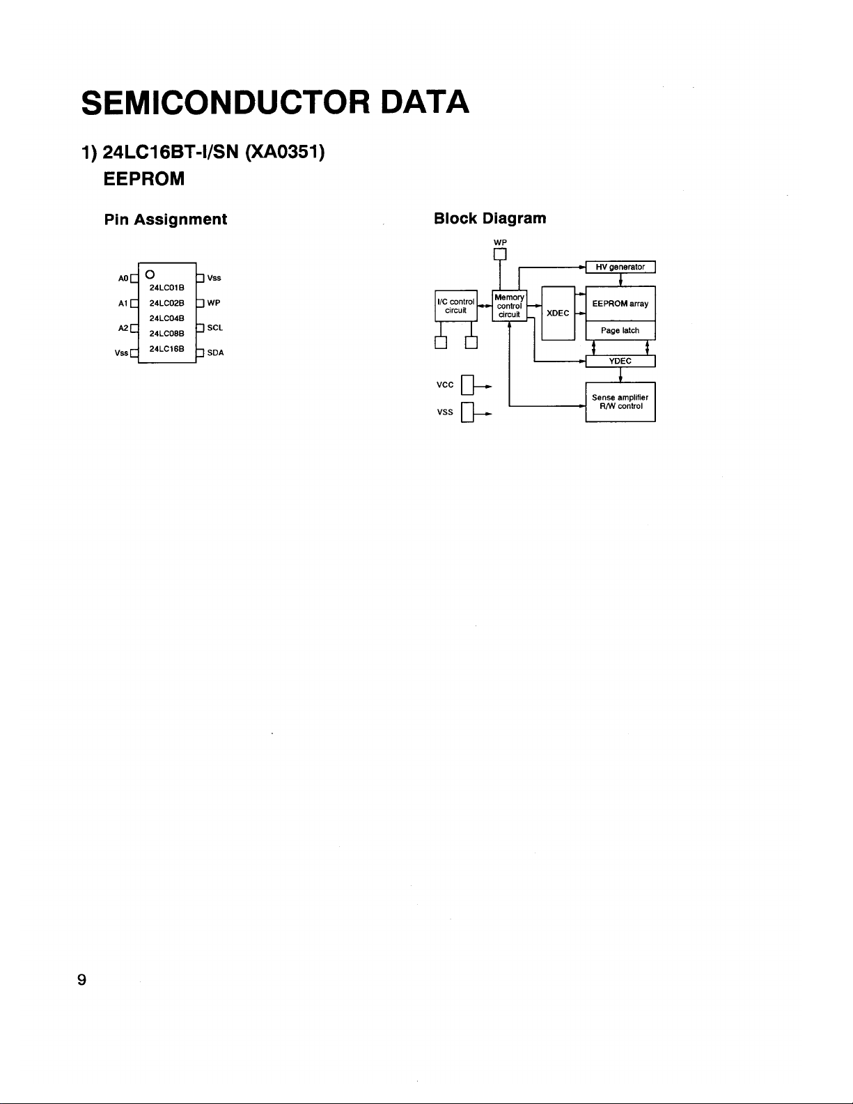
+SEMICONDUCTOR DATA
9
+EXPLODED VIEW
15
+PARTS LIST
18
+ADJUSTMENT
21
+PCBOARD VIEW
26
+CIRCUIT DIAGRAM
36
+BLOCK DIAGRAM
43
ALINCO INCORPORATED
e-mail: export@alinco.co.jp
TWIN 21 M.I.D. TOWER BUILDING 23F, 1-61, 2-CHOME,
SHIROMI CHUO-KU , OSAKA, 540-8580 JAPAN
Tel (81)6-6946-8150 fax (81)6-6946-8175
Page 2

SPECIFICATIONS
Frequency Coverage
TX
RX
DJ-190T (u.s. Amateur version)
144.000 ~ 147.995MHz 135.000 ~ 173.995MHz
DJ-190E (European Amateur version)
144.000 ~ 145.995MHz 144.000 ~ 145.995MHz
DJ-190TA1 (commercial version VHFL)
135.000 ~ 155.000MHz 135.000 ~ 173.995MHz
DJ-190TA2 (commercial version VHFH)
150.000 ~ 173.995MHz 135.000 ~ 173.995MHz
Channel Step:
5, 10, 12.5, 15, 20, 25, 30kHzsteps
Memory Channels:
40 Channels
Antenna Impedance:
50ohm unbalanced
Frequency Stability:
+/-5 ppm
Microphone Input Impedance:
2kohm nominal.
Signal Type:
F3E (FM)
Offset Range:
0 ~ 99.995MHz
Deviation:
15kHz max.
TX Output (supply voltage):
1.5W (4.8V) / 3.5W (7.2V) / 5W (9.6 ~ 13.8V)
RX Sensitivity:
12dB SINAD better than - 16dBu
RX Selectivity:
-6dB/ +/- 12kHz
I.F.:
(1st) 21.25MHz / (2nd) 450kHz
Power Supply Requirements:
4.8 ~ 13.8V DC (4.8V DC standard)
Current Consumption
Transmitting: Approx. 1.2 Amp. in High Power
at 13.8V DC:
Setting
Receiving: Squelched Approx. 24mA (BS on)
Operating Temperature:
-10 ~ +60*C, 14 ~ 140*F
Dimensions:
57(W) x 151(H) x 27(D) mm
(with EBP-37N without projections)
2 1/4(W) x 6(H) x 1 1/16(D) inches
Weight:
Approx. 300g
Subaudible Tones (CTCSS) :
Encoder installed (50 tones)
Page-2
Page 3

CIRCUIT DESCRIPTION
1) Receiver System
The receiver system is a double superheterodyne system with a 21.7 MHz
first IF and a450 kHz second IF.
1. Front End
The received signal at any frequency in the 130.00- to 173.995-MHz range
is passed through the low-pass filter (L102, L103, L104, C113, C107, C116,
and C114) and tuning circuit (L112 and D107), and amplified by the RF
amplifier (Q107). The signal from Q107 is then passed through the tuning
circuit (L109, L110, L111, and varicapsi D104, D105 and D106) and
converted into 21.7 MHz by the mixer (Q106). The tuning circuit, which
consists of L112, L109, varicaps D107 and D104, Ll110 L111, varicaps
D105 and D106, is controlled by the tracking voltage from the CPU so that
it is optimized for the reception frequency. The local signal from the VCO is
passed through the buffer (Q108), and supplied to the source of the mixer
(Q106). The radio uses the lower side of the superheterodyne system.
2. IF Circuit
The mixer mixes the received signal with the local signal to obtain the sum
of and difference between them. The crystal filter (XF101 , XF102) selects
21.7 MHz frequency from the results and eliminates the signals of the
unwanted frequencies. The first IF amplifier (Q105) then amplifies the
signal of the selected frequency.
3. Demodulator Circuit
After the signal is amplified by the first IF amplifier (Q105), it is input to pin
16 of the demodulator IC (IC104). The second local signal of 21.25 MHz
(shared with PLL IC reference oscillation), which is oscillated by the internal
oscillation circuit in IC102 and crystal (X101), is input through pin 1 of
IC104. Then, these two signals are mixed by the internal mixer in IC104
and the result is converted into the second IF signal with a frequency of 450
kHz. The second IF signal is output from pin 3 of IC104to the ceramic filter
(FL101), where the unwanted frequency band of that signal is eliminated,
and the resulting signal is sent back to the IC104 through pins 5 and 7.
The second IF signal input via pin 7 is demodulated by the internal limiter
amplifier and quadrature detection circuit in IC104, and output as an audio
signal through pin 9.
4. Audio Circuit
The audio signal from pin 9 of IC104 is compensated to the audio
frequency characteristics in the de-emphasis circuit (R162, R161, C172,
C173) and amplified by the AF amplifier (Q109). The signal is then input to
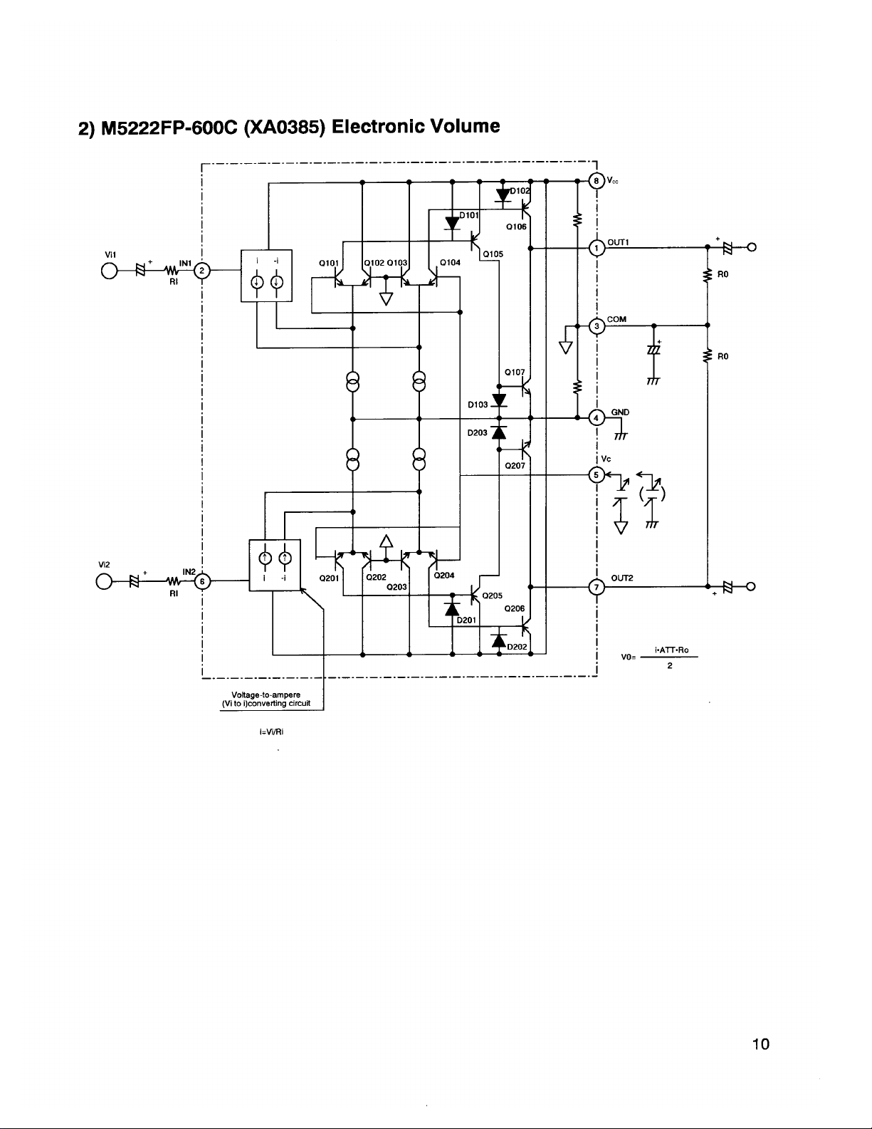
pin 2 of the electronic volume (IC103) for volume adjustment, and output
from pin 1. The adjusted signal is sent to the audio power amplifier (1C105)
through pin 2 to drive the speaker.
5. Squelch Circuit
Part of the audio signal from pin 9 of IC104 is amplified by the noise filter
amplifier consisting of R176, R186, R177, C179, C183, C191, and C194,
and the internal noise amplifier in IC104. The desired noise of the signal is
output through pin 11 of IC104, to be further amplified by the noise amplifier
(Q115). The amplified noise signal is rectified by voltage doublers D109 and
input to pin 4 of CPU (IC5).
Page-3
Page 4

2) Transmitter System
The audio signal is converted to an electric signal in either the internal or
1. Modulator Circuit
external microphone, and input to the microphone amplifier (IC6). IC6
consists of two operational amplifiers; one amplifier (pins 1, 2, and 3) is
composed of pre-emphasis and IDC circuits and the other (pins 5, 6, and 7)
is composed of a splatter filter. The maximum frequency deviation is
determined to its optimal value by switch circuits consisting of Q9 and Q10
and input to the cathode of the varicap of the VCO, to change the electric
capacity in the oscillation circuit. This produces the frequency modulation.
2. Power Amplifier
The transmitted signal is oscillated by the VCO, amplified by the pre-drive
Circuit
amplifier (Q102) and drive amplifier (Q101), and input to the power module
(IC101). The signal is then amplified by the power module (IC101) and led
to the antenna switch (D101) and low-pass filter (L102, L103, L104, C113,
C107, C116, and C114), where unwanted high harmonic waves are
reduced as needed, and the resulting signal is supplied to the antenna.
3. APC Circuit
Part of the transmission power from the low-pass filter is detected by D103,
converted to DC, and then amplified by a differential amplifier. The output
voltage controls the bias voltage from pin 2 of the power module (IC101) to
maintain the transmission power constant.
3) PLL Synthesizer Circuit
The dividing ratio is obtained by sending data from the CPU (IC5) to pin 2
1.PLL
and sending clock pulses to pin 3 of the PLL IC (IC102). The oscillated
signal from the VCO is amplified by the buffer (Q117) and input to pin 6 of
IC102. Each programmable divider in IC102 divides the frequency of the
input signal by N according to the frequency data, to generate a
comparison frequency of 5 or 6.25 kHz.
2. Reference Frequency
The reference frequency appropriate for the channel steps is obtained by
Circuit
dividing the 21.25 MHz reference oscillation (X101) by 4250 or 3400,
according to the data from the CPU (IC5). When the resulting frequency is
5 kHz, channel stepsof5, 10, 15, 20, 25 and 30 kHz are used. When it is
6.25 kHz, the 12.5 kHz channel step is used.
3. Phase Comparator
The PLL (IC102) uses the reference frequency, 5 or 6.25 kHz. The phase
Circuit
comparator in the IC102 compares the phase of the frequency from the
VCO with that of the comparison frequency, 5 or 6.25 kHz, which is
obtained by the internal divider in IC102
4. PLL Loop Fitter Circuit
If a phase difference is found in the phase comparison between the
reference frequency and VCO output frequency, the charge pump output
(pin 8) of IC102 generates a pulse signal, which is converted to DC voltage
by the PLL loop filter and input to the varicap of the VCO unit for oscillation
frequency control.
Page-4
Page 5

5. VCO Circuit
A Colpitts oscillation circuit driven by Q301 directly oscillates the desired
frequency. The frequency control voltage determined in the CPU (IC5) and
PLL circuit is input to the varicaps (D301 and D304). This changes the
oscillation frequency, which is amplified by the VCO buffer (Q302) and
output from the VCO unit.
Note
The oscillation frequency is determined by turning Q301 0N and OFF.
Displayed frequencies
Q301
TX: 130.00 - 139.995 MHz
OFF
RX: 130.00 - 161.695 MHz
TX: 140.00 - 173.995 MHz
ON
RX: 161.70 - 173.995 MHz
4) CPU and Peripheral Circuits
The CPU turns ON the LCD via segment and common terminals with 1/3
1. LCD Display Circuit
the duty and 1/3 the bias, at the frame frequency is 85Hz.
2. Display Lamp Circuit
When the LAMP key is pressed, "H" is output from pin 45 of CPU (IC5) to
the bases of Q1 then turn ON and the LEDs (D1, D3) Bight.
3. Reset and Backup
When the power from the DC jack or external battery increases from 0 V to
Circuits
2.5 or more, "H" level reset signal is output from the reset IC (IC2) to pin 35
of the CPU (IC5), causing the CPU to reset. The reset signal. however,
waits at C6 and R98, and does not enter the CPU until the CPU clock (X1)
has stabilized. When the external power drops to 3.2 V or below, the output
signal from the backup IC (IC3), which has been input to pin 34 of the CPU,
changes from "H" to "L" level. The CPU will then be in the backup state.
4. S(Signal)Meter Circuit
The DC potential of pin 13 of IC104 is input to pin 3 of the CPU (IC5),
converted from an analog to a digital signal, and displayed as the S-meter
signal on the LCD.
5. Tone Encoder
The CPU (IC5) is equipped with an internal tone encoder. The tone signal
(67.0 to 254.1 Hz) is output from pin 11 of the CPU to the varicap of the
VCO for modulation.
Page-5
Page 6

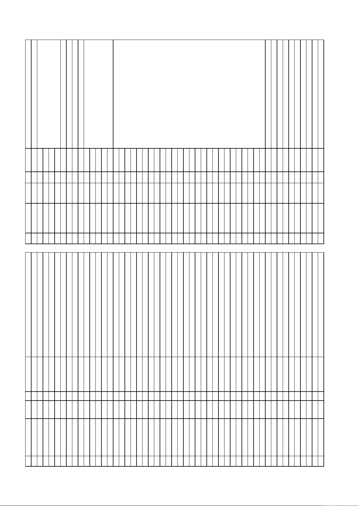
5) CPU Terminal Functions: M38267M8L (XA413)
Page-6
Page 7
No.
Pin Name
Signal
I/0
Logic
Description
No.
Pin Name
Signa1
I/0
Logic
Description
1
C1C1---51P15/SEG39
F/KEY
I
Active low
Function key input
2
VL1
VL1IA/D
LCDpowersupply
52
P14/SEG38
K10I-3P67/AN7
SMTIA/D
S-meterinput
53
P13/SEG37
K11I-4P66/AN6
SQLIA/D
Noise level input for squelch
54
P12/SEG36
K12I-5P65/AN5
BATIA/D
Low battery detection input
55
P11/SEG35
K13l-6P64/AN4
BP5IA/D
Band plan5
56
P11/SEG34
K14I-
Key matrix input
7
P63/CLK22/AN3
BP4IBand plan4
57
P07/SEG33
SFTO-
VCO frequency range change
8
P62/CLK21/AN2
ULIActivehigh
PLL unlock signal input
58
P06/SEG32
SDOActive low
Signa detection output
9
P61/SOUT2/AN1
BP1,2IA/D
Band plans 1 and 2
59
P05/SEG31
AFCOActive high
AF tone control output
10
P60/SIN2/ANO
MOMIActivelow
Monitor key input
60
P04/SEG30
DA4O-11P57/ADT/DA2
CTOUT
O
D/A
CTCSS tone output
61
P03/SEG29
DA3O-12P56/AD1
DTOUT
O
D/A62P02/SEG28
DA2O-
DA converter for electronic volume and output power
13
P55/CNTR1
TSQDIActivelow
CTCSS tone detection input
63
P01/SEG27
DA1O-14P54/CNTRO
BEPOPulse
Beep tone output/Band plan 3
64
P00/SEG26
DA0O-15P53/RTP1
STB2
I/O
Active low/pulse
CTCSS unit detection/Strobe signal to CTCSS unit
65
P37/SEG25
S25O-16P52/RTP0
MUTE
I/O
Activehigh
Microphone mute
66
P36/SEG24
S24O-17P51/PWM1
CLKOPulse
Serial clock output for PLL, CTCSS
67
P35/SEG23
S23O-18P50/PWM0
DATAOPulse
Serial data output for PLL CTCSS
68
P34/SEG22
S22O-19P47/SRDY1
ACK
I/0
Pulse
Band plan 6
69
P33/SEG21
S21O-20P46/SCLK1
STB1OPulse
Strobe for PLL IC
70
P32/SEG20
S20O-21P45/TXD1
UTXOPulse
UART data transmission output
71
P31/SEG19
S19O-22P44/RXD1
URXIPulse
UART data reception input
72
P30/SEG18
S18O-23P43/D/TOUT
TBSTOPulse
Tone burst (1750Hz) output (European version)
73
SEG17
S17O-24P42/INT2
RE2IActivelow
74
SEG16
S16O-25P41/1NT1
RE1IActivelow
Rotary encoder lnput
75
SEG15
S15O-26P40
PTTIActivehigh
PTT input
76
SEG14
S14O-27P77
DSWOActivelow
77
SEG13
S13O-28P76
STD
I/O
Activehigh
Deviation adjustment during transmission
78
SEG12
S12O-
LCD segment signal
29
P75
DSDIPulse
Deviation adjustment during transmission
79
SEG11
S11O-30P74
T3COActive low
TX power ON/OFF output
80
SEG10
S10O-31P73
P3COActive low
PLL power ON/OFF output
81
SEG9S9O
-32P72
AFPOActivelow
AFAMP power ON/OFF output
82
SEG8S8O
-33P71
R3COActivelow
RX power ON/OFF output
83
SEG7S7O
-34P70/INT0
BUIActivelow
Backup signal detection input
84
SEG6S6O
-35RESET
RSTIActivelow
Resetinput
85
SEG5S5O
-36XCIN
XCIN---86
SEG4S4O
-37XCOUNT
XCOUT
---87SEG3S3O
-38XIN
XIN--
Main clock input
88
SEG2S2O
-39XOUT
XOUT--
Main clock output
89
SEG1S1O
-40VSS
GND--
CPU ground
90
SEG0SOO
-41P27
PSWIActivelow
Power switch input
91
VCC
VDD--
CPU power terminal
42
P26
SCLOPulse
Serial clock for EEPROM
92
VREF
VREF--
AD converter power supply
43
P25
C3COActivehigh
C3 power ON/OFF output
93
AVSS
AVSS--
AD converter ground
44
P24
SDAOPulse
Serial data for EEPROM
94
COM3
COM3--
-45P23
LMPOActivehigh
Lamp ON/OFF
95
COM2
COM2O-
LCD COM2 output
46
P22
T/KEY
I
Activelow
Tone burst/LPTT input
96
COM1
COM1O-
LCD COM1 output
47
P21
K00
I/O-Band plan BP7 input
97
COM0
COM0O-
LCD COM0 output
48
P20
K01O-
Key matrix output
98
VL3
VL3I-
LCD power supply
49
P17
K02O-99VL2
VL2I-
LCD power supply
50
P16
K03O-
100C2I--
Page-7
Page-8
Page 8
Page 9
Page 10

Page 11

Page 12

Page 13

Page 14

Page 15

Page 16

Page 17

PARTS LIST
CPU Unit/Tone Unit
Ref.No.
PartsNo.
Description
Parts Name
Ver.
Ref.No.
PartsNo.
Description
Parts Name
Ver.
Ref.No.
Parts No.
Description
Parts Name
Ver.
Ref.No.
PartsNo.
Description
Parts Name
Ver.
CPU unit
IC5
XA0402
IC
M38267M8L-l01FP
R35
RK3058
Chip R
ERJ3GSYJ473V
R1001
RK3046
Chip R
ERJ3GSYJ472V
C1
CU3035
Chip C
C1608JB1H102KTA
IC6
XA0209
IC
NJM2100M T1
R36
RK1018
Chip R
ERJ8GEYJ101V
R1002
RK3048
Chip R
ERJ3GSYJ682V
C2
CU3035
Chip C
C1608JB1H102KTA
J1
MACL2GG
Wire
#30A11l-025-H1
R37
RK3038
Chip R
ERJ3GSYJ102V
R1003
RK3062
Chip R
ERJ3GSYJ104V
C3
CS0206
Chip Tantal
TMCMD0G107MTR
JK1
UJ0019
Connector
HSJ1493-01-010
R38
RK3041
Chip R
ERJ3GSYJ182V
R1005
RK3058
Chip R
ERJ3GSYJ473V
C4
CU3017
Chip C
C1608CH1H330JT-AS
JK2
UJ0022
Connector
HSJ1102-01-540
R39
RK3038
Chip R
ERJ3GSYJ102V
R1006
RK3038
Chip R
ERJ3GSYJ102V
C5
CU3017
Chip C
C1608CH1H330JT-AS
L1
QC0003
Coil
MLF3216A1R0K-T
R40
RK3068
Chip R
ERJ3GSyJ334V
R1007
RK3038
Chip R
ERJ3GSYJ102V
C6
CS0208
Chip Tantal
TMCMA0J475MTR
L2
QC0003
Coil
MLF3216A1R0K-T
R41
RK3065
Chip R
ERJ3GSYJ184V
R1008
RK3001
Chip R
ERJ3GSY0R00V
C7
CU3035
Chip C
C1608JB1H102KTA
L4
QC0003
Coil
MLF3216A1R0K-T
R42
RK3061
Chip R
ERJ3GSYJ823V
R1009
RK3038
Chip R
ERJ3GSYJ102V
C8
CU3035
Chip C
C1608JB1H102KTA
L5
QC0003
Coil
MLF3216A1R0K-T
R43
RK3058
Chip R
ERJ3GSYJ473V
R1010
RK3058
Chip R
ERJ3GSYJ473V
C9
CS0206
Chip Tantal
TMCMD0G107MTR
L6
QC0442
Coil
MLF1608A1R0K-T
R44
RK3054
Chip R
ERJ3GSYJ223V
R1011
RK3038
Chip R
ERJ3GSYJ102V
C10
CS0373
Chip Tantal
TMCMD1C476MTR
L7
QC0442
Coil
MLF1608A1R0K-T
R47
RK3052
Chip R
ERJ3GSYJ153V
R1012
RK3038
Chip R
ERJ3GSYJ102V
C11
CS0206
Chip Tantal
TMCMD0G107MTR
L8
QC0442
Coil
MLF1608A1R0K-T
R48
RK3062
Chip R
ERJ3GSYJ104V
R1013
RK3001
Chip R
ERJ3GSY0R00V
C12
CU3059
Chip C
C1608JF1E104ZTA
L9
QC0442
Coil
MLF1608A1R0K-T
R49
RK3048
Chip R
ERJ3GSYJ682V
X1
XQ0074
Crystal
SMD-49 4.19MHZ
C16
CS0057
Chip Tantal
TMCSA0J225MTR
L10
QC0442
Coil
MLF1608A1R0K-T
R52
RK3041
Chip R
ERJ3GSYJ182V
UP0294B
P.C.B
CPU PCB
C18
CS0049
Chip Tantal
TMCSA1C105MTR
LCD1
EL0030
LCD
LCD XH618
R53
RK3046
Chip R
ERJ3GSYJ472V
TL0016
Spread Sheet DJG5
C19
CU3021
Chip C
C1608CH1H680JTA
MIC1
EY0012
Mic
EN-123T
R54
RK3062
Chip R
ERJ3GSYJ104V
FG0186Z
Jack Cap
C20
CU3035
Chip C
C1608JB1H102KTA
Q1
XU0064
Transistor
UN5210 TX
R55
RK3050
Chip R
ERJ3GSYJ103V
DG0021
LCD Light DJG5
C21
CU3056
Chip C
C1608JF1E473ZTA
Q3
XU0040
Transistor
UN211H TX
R56
RK3066
Chip R
ERJ3GSYJ224y
FG0182
LCD Rubber(A)DJG5
C22
CU3035
Chip C
C1608JB1H102KTA
Q5
XU0040
Transistor
UN211H TX
R57
RK3039
Chip R
ERJ3GSYJ122V
FG0183
LCD Rubber(B)DJG5
C23
CU3035
Chip C
C1608JB1H102KTA
Q7
XU0014
Transistor
DTC144EKA T146
R58
RK3069
Chip R
ERJ3GSyJ394V
C24
CU3051
Chip C
C1608JB1E223KTA
Q9
XU0064
Transistor
UN5210 TX
R59
RK3051
Chip R
ERJ3GSYJ123V
ST0053Y
LCD Holder DJ190
C25
CU3051
Chip C
C1608JB1E223KTA
Q10
XU0064
Transistor
UN5210 TX
R60
RK3038
Chip R
ERJ3GSYJ102V
FG0234
Mic Holdcr
C26
CU3027
Chip C
C1608CH1H221JTA
Q11
XT0095
Transistor
2SC4081 T106R
R61
RK3054
Chip R
ERJ3GSYJ223V
TZ0072
Sheet Insulator
C27
CU3035
Chip C
C1608JB1H102KTA
Q12
XU0064
Transistor
UN5210 TX
R62
RK3065
Chip R
ERJ3GSYJ184V
UR0012
Switch
C29
CU3027
Chip C
C1608CH1H221JTA
Q13
XU0064
Transistor
UN5210 TX
R63
RK3056
Chip R
ERJ3GSYJ333V
Tone Unit (EJ-28U)
C30
CU3059
Chip C
C1608JF1E104ZTA
R1
RK3028
Chip R
ERJ3GSYJ151V
R64
RK3058
Chip R
ERJ3GSYJ473V
C701
CU3015
Chip C
C1608CH1H220JTA
C31
CS0063
Chip Tantal
TMCSA1V104MTR
R3
RK3028
Chip R
ERJ3GSYJ151V
R65
RK3058
Chip R
ERJ3GSYJ473V
C702
CU3015
Chip C
C1608CH1H220JTA
C32
CU3035
Chip C
C1608JB1H102KTA
R4
RK3050
Chip R
ERJ3GSYJ103V
R66
RK3055
Chip R
ERJ3GSYJ273V
C703
CU3023
Chip C
C1688CH1H101JTA
C33
CU3035
Chip C
C1608JB1H102KTA
R5
RK3038
Chip R
ERJ3GSYJ102V
R67
RK3046
Chip R
ERJ3GSYJ472V
C705
CS0237
Chip Tantal
TMCMA1A475MTR
C35
CU3035
Chip C
C1608JB1H102KTA
R6
RK3058
Chip R
ERJ3GSYJ473V
R68
RK3061
Chip R
ERJ3GSyJ823V
C709
CS0049
Chip Tantal
TMCSA1C105MTR
C36
CU3035
Chip C
C1608JB1H102KTA
R7
RK3038
Chip R
ERJ3GSYJ102V
R69
RK3050
Chip R
ERJ3GSYJ103V
C710
CU3059
Chip C
C1608JF1E104ZTA
C37
CU3026
Chip C
C1608CH1H181JT-AS
R8
RK3046
Chip R
ERJ3GSYJ472V
R70
RK3062
Chip R
ERJ3GSYJ104V
C711
CS0236
Chip Tantal
TMCMA0J685MTR
C38
CS0049
Chip Tantal
TMCSA1C105MTR
R9
RK3058
Chip R
ERJ3GSYJ473V
R71
RK3034
Chip R
ERJ3GSyJ471V
C712
CU3035
Chip C
C1608JB1H102KTA
C39
CU3059
Chip C
C1608JF1E104ZTA
R10
RK3058
Chip R
ERJ3GSYJ473V
R72
RK3056
Chip R
ERJ3GSyJ333V
C713
CU3019
Chip C
C1608CH1H470JTA
C40
CU3059
Chip C
C1608JF1E104ZTA
R11
RA0003
Chip R
NNRl4E0AJl02E
R73
RK3051
Chip R
ERJ3GSVJ123V
C714
CS0049
Chip Tantal
TMCSA1C105MTR
C41
CU3059
Chip C
C1608JF1E104ZTA
R12
RK3038
Chip R
ERJ3GSYJ102V
R75
RK3058
Chip R
ERJ3GSYJ473V
C715
CS0049
Chip Tantal
TMCSA1C105MTR
C43
CS0063
Chip Tantal
TMCSA1V104MTR
R13
RK3038
Chip R
ERJ3GSYJ102V
R76
RK3038
Chip R
ERJ3GSYJ102V
CN701
UE0274
AXN320C038P
C44
CU3047
Chip C
C1608JB1H103KTA
R14
RK3038
Chip R
ERJ3GSYJ102V
R78
RK3038
Chip R
ERJ3GSYJ102V
UP0295A
EJ28U PCB
C45
CU3035
Chip C
C1608JB1H102KTA
R15
RK3024
Chip R
ERJ3GSYJ680V
R79
RK3001
Chip R
ERJ3GSY0R00V
E
R701
RK3048
Chip R
ERJ3GSYJ682V
C47
CU3059
Chip C
C1608JF1E104ZTA
R16
RK3024
Chip R
ERJ3GSYJ680V
R80
RK3046
Chip R
ERJ3GSYJ472V
R702
RK3089
Chip R
ERJ3GSYJ912V
C48
CU3059
Chip C
C1608JF1E104ZTA
R18
RK3036
Chip R
ERJ3GSyJ681V
R82
RK3058
Chip R
ERJ3GSYJ473V
R703
RK3066
Chip R
ERJ3GSYJ224V
CN3
UP0282
DJG5 lF-RF
R19
RK3074
Chip R
ERJ3GSYJ105V
R83
RK3058
Chip R
ERJ3GSYJ473V
R704
RK3074
Chip R
ERJ3GSYJ105V
CN4
UE0144
TE1208P128G02
R20
RK3038
Chip R
ERJ3GSYJ102V
R84
RK3038
Chip R
ERJ3GSYJ102V
E
R705
RK3051
Chip R
ERJ3GSYJ123V
CN7
UE0267
AXN420C330P
R21
RK3038
Chip R
ERJ3GSYJ102V
R86
RK3058
Chip R
ERJ3GSYJ473V
R707
RK3067
Chip R
ERJ3GSYJ274V
D1
XL0045
LED
PG1101F-TR
R22
RK3074
Chip R
ERJ3GSYJ105V
R87
RK3046
Chip R
ERJ3GSYJ472V
R710
RK3047
Chip R
ERJ3GSYJ562V
D3
XL0045
LED
PG1101F-TR
R23
RK3043
Chip R
ERJ3GSYJ272V
R89
RK3038
Chip R
ERJ3GSYJ102V
R715
RK3060
Chip R
ERJ3GSYJ683V
D7
XD0291
Diode
MA729-TX
R24
RK3038
Chip R
ERJ3GSYJ102V
R92
RK3001
Chip R
ERJ3GSY0R00V
R716
RK3054
Chip R
ERJ3GSYJ223V
D9
XD0291
Diode
MA729-TX
R26
RK3038
Chip R
ERJ3GSYJ102V
R93
RK3042
Chip R
ERJ3GSYJ222V
R717
RK3055
Chip R
ERJ3GSYJ273V
D10
XL0046
LED
VRPG4607K
R28
RK3058
Chip R
ERJ3GSYJ473V
R94
RK3030
Chip R
ERJ3GSYJ221V
R718
RK3062
Chip R
ERJ3GSYJ104V
D11
XD0250
Diode
MA742 TX
R30
RA0003
Chip R
MNR14E0AJ102E
R95
RK3030
Chip R
ERJ3GSYJ221V
IC701
XA0239
IC
AK2341
IC1
XA0351
IC
24LC16BT-1/SN
R31
RK3055
Chip R
ERJ3GSYJ273V
R96
RK3038
Chip R
ERJ3GSYJ102V
XQ0077
Crystal
38C 3.686400MHZ
IC2
XA0309
IC
RH5VL25AA-T1
R32
RK3058
Chip R
ERJ3GSYJ473V
R97
RK3038
Chip R
ERJ3GSYJ102V
TZ0069
EJ28U
IC3
XA0198
IC
RH5VL32AA-T1
R33
RK3058
Chip R
ERJ3GSYJ473V
R98
RK3070
Chip R
ERJ3GSYJ474V
HK0398A
Package
IC4
XA0383
IC
S-81235SG-Q1-T1
R34
RK3058
Chip R
ERJ3GSYJ473V
R99
RK3001
Chip R
ERJ3GSY0R00V
E
HP0029
Protec.Bag
Page 18
Page 18

RF Unit
RF Unit
Ref.No.
Parts No.
Description
Parts Name
Ver.
Ref.No.
Parts No.
Description
Parts Name
Ver.
Ref.No.
Parts No.
Descrlptlon
Parts Name
Ver.
Ref.No.
Parts No.
Description
Parts Name
Ver.
RF Unit
C152
CU3015
Chip C
C1608CH1H220JTA
C204
CU3059
Chip C
C1608JF1E104ZTA
Q105
XT0096
Transistor
2SC4099 T106N
C101
CU3035
Chip C
C1608JB1H102KTA
C153
CU3017
Chip C
C1608CH1H330JTA
C205
CE0373
Ek!ctrQlytic C
16XV 100UV
Q106
XE0020
FET
2SK3601GE TL
C102
CU3035
Chip C
C1608JB1H102KTA
C154
CU3018
Chip C
C1608CH1H390JTA
C206
CS0366
Chip Tantal
TMCMA0G106MTR
Q106
XE0009
FET
2SK302GR
C103
CU3035
Chip C
C1608JB1H102KTA
C155
CU3017
Chip C
C1608CH1H330JTA
C215
CU3035
Chip C
C1608JB1H102KTA
Q107
XT0137
Transistor
2SC5065-O(TE85L)
C104
CU3035
Chip C
C1608JB1H102KTA
C156
CU3035
Chip C
C1608JB1H102KTA
C216
CU3035
Chip C
C1608JB1H102KTA
Q108
XT0096
Transistor
2SC4099 T106N
C105
CU3035
Chip C
C1608JB1H102KTA
C157
CU3007
Chip C
C1608CH1H060CTA
C217
CU3019
Chip C
C1608CH1H470JTA
Q109
XT0095
Transistor
2SC4081 T106R
C106
CU3017
Chip C
C1608CH1H330JTA
C158
CU3035
Chip C
C1608JB1H102KTA
C218
CU3035
Chip C
C1608JB1H102KTA
Q110
XT0088
Transistor
2SA1213Y TE12R
C107
CU3010
Chip C
C1608CH1H090CTA
C159
CU3059
Chip C
C1608JF1E104ZTA
C219
CS0366
Chip Tantal
TMCMA0G106MTR
Q111
XT0088
Transistor
2SA1213Y TE12R
C107
CU3007
Chip C
C1608CH1H060CTA
TA2
C160
CU3047
Chip C
C1608JB1H103KTA
C220
CS0063
Chip Tantal
TMCSA1V104MTR
Q112
XU0027
Transistor
FMA7AT148
C108
CU3007
Chip C
C1608CH1H060CTA
TA2
C161
CU3047
Chip C
C1608JB1H103KTA
C223
CU3035
Chip C
C1608JB1H102KTA
Q113
XU0172
Transistor
XP1501-TX
C110
CU3017
Chip C
C1608CH1H330JTA
C163
CS0377
Chip Tantal
TMCMB0G476MTR
C224
CU3015
Chip C
C1608CH1H220JTA
Q114
XT0088
Transistor
2SA1213Y TE12R
C112
CU3011
Chip C
C1608CH1H100CTA
C164
CS0049
Chip Tantal
TMCSA1C105MTR
C225
CU3035
Chip C
C1608JB1H102KTA
Q115
XT0095
Transistor
2SC4081 T106R
C113
CU3017
Chip C
C1608CH1H330JTA
C165
CU3021
Chip C
C1608CH1H680JTA
C226
CS0049
Chip Tantal
TMCSA1C105MTR
Q116
XU0172
Transistor
XP1501-TX
C113
CU3013
Chip C
C1608CH1H150JTA
TA2
C166
CU3059
Chip C
C1608JF1E104ZTA
C228
CS0377
Chip Tantal
TMCMB0G476MTR
Q117
XT0137
Transistor
2SC5065-O(TE85L)
C114
CU3019
Chip C
C1608CH1H470JTA
C167
CU3016
Chip C
C1608CH1H270JTA
C229
CS0237
Chip Tantal
TMCMA1A475MTR
Q118
XU0125
Transistor
DTA144EUAT106
C114
CU3013
Chip C
C1608CH1H150JTA
TA2
C168
CU3015
Chip C
C1608CH1H220JTA
C230
CS0366
Chip Tantal
TMCMA0G106MTR
Q119
XU0038
Transistor
UN2214 TX
C115
CU3013
Chip C
C1608CH1H150JTA
C169
CS0049
Chip Tantal
TMCSA1C105MTR
D101
XD0066
Diode
RLS135 TE 11
Q120
XU0062
Transistor
UN9111 TX
C116
CU3019
Chip C
C1608CH1H470JTA
C170
CU3056
Chip C
C1608JF1E473ZTA
D102
XD0066
Diode
RLS135 TE 11
R101
RK3028
Chip R
ERJ3GSYJ151V
C116
CU3012
Chip C
C1608CH1H120JTA
TA2
C171
CU3059
Chip C
C1608JF1E104ZTA
D103
XD0251
Diode
MA741WA TX
R102
RK3026
Chip R
ERJ3GSYJ101V
C117
CS0049
Chip Tantal
TMCSA1C105MTR
C172
CU3051
Chip C
C1608JB1E223KTA
D104
XD0299
Diode
MA304-TX
R103
RK3026
Chip R
ERJ3GSYJ101V
C118
CU3035
Chip C
C1608JB1H102KTA
C173
CU3053
Chip C
C1608JF1E333ZTA
D105
XD0299
Diode
MA304-TX
R104
RK3034
Chip R
ERJ3GSYJ47lV
C119
CU3035
Chip C
C1608JB1H102KTA
C174
CU3047
Chip C
C1608JB1H103KTA
D106
XD0299
Diode
MA304-TX
R105
RK3046
Chip R
ERJ3GSYJ472V
C121
CU3004
Chip C
C1608CH1H030CTA
C175
CS0382
Chip Tantal
TMCMB1A226MTR
D107
XD0299
Diode
MA304-TX
R106
RK3050
Chip R
ERJ3GSYJ103V
C121
CU3003
Chip C
C1608CH1H020CTA
TA2
C176
CU3059
Chip C
C1608JF1E104ZTA
D108
XD0129
Diode
1SS318 TT11
R107
RK3046
Chip R
ERJ3GSYJ472V
C122
CU3004
Chip C
C1608CH1H030CTA
C177
CS0220
Chip Tantal
TMCMA1C225MTR
D109
XD0118
Diode
MA716 TX
R108
RK3046
Chip R
ERJ3GSYJ472V
C122
CU3003
Chip C
C1608CH1H020CTA
TA2
C178
CU3035
Chip C
C1608JB1H102KTA
D113
XD0130
Diode
DA204U T106
R110
RK3026
Chip R
ERJ3GSYJ101V
C123
CU3015
Chip C
C1608CH1H220JTA
C179
CU3027
Chip C
C1608CH1H221JTA
FL101
XC0018
Filter
CFWM450E
R111
RK3026
Chip R
ERJ3GSYJ101V
C124
CU3035
Chip C
C1608JB1H102KTA
C180
CU3035
Chip C
C1608JB1H102KTA
JK101
RD0108
JPV01R-0l
R113
RK3050
Chip R
ERJ3GSYJ103V
C125
CU3002
Chip C
C1608CH1H010CTA
C181
CU3059
Chip C
C1608JF1E104ZTA
IC101
XA0381
IC
S-AV28
R113
RK3051
Chip R
ERJ3GSYJ123V
TA2
C126
CU3002
Chip C
C1608CH1H010CTA
C182
CU3035
Chip C
C1608JB1H102KTA
IC101
XA0421
IC
PF0311
TA2
R114
RK3050
Chip R
ERJ3GSYJ103V
C127
CS0049
Chip Tantal
TMCSA1C105MTR
C183
CU3035
Chip C
C1608JB1H102KTA
IC102
XA0352
IC
X64076GP
R115
RK3026
Chip R
ERJ3GSYJ101V
C128
CU3035
Chip C
C1608JB1H102KTA
C184
CU3035
Chip C
C1608JB1H102KTA
IC103
XA0385
IC
M5222FP-600C
R116
RK3050
Chip R
ERJ3GSYJ103V
C129
CU3035
Chip C
C1608JB1H102KTA
C185
CU3047
Chip C
C1608JB1H103KTA
IC104
XA0343
IC
MC3372VX-EL
R117
RK3034
Chip R
ERJ3GSYJ471V
C130
CS0220
Chip Tantal
TMCMA1C225MTR
C186
CE0308
6.3CV100BS
IC105
XA0210
IC
NJK2070XT1
R118
RK3050
Chip R
ERJ3GSYJl03V
C131
CU3051
Chip C
C1608JB1E223KTA
C187
CU3035
Chip C
C1608JB1H102KTA
L101
QC0016
Coil
MLF3216A2R2K-T
R118
RK3051
Chip R
ERJ3GSYJ123V
TA2
C132
CU3047
Chip C
C1608JB1H103XTA
C188
CS0049
ChipTanta1
TMCSA1C105MTR
L102
QKA65A
Coil
XRl.5 3.5T 0.4
R119
RK3038
Chip R
ERJ3GSYJ102V
C133
CU3047
Chip C
C1608JB1H103KTA
C189
CU3047
Chip C
C1608JB1H103KTA
L103
QKA65A
Coil
MR1.5 3.5T 0.4
R121
RK3050
Chip R
ERJ3GSYJ103V
C134
CU3035
Chip C
C1608JB1H102KTA
C190
CU3059
Chip C
C1608JF1E104ZTA
L104
QKA65A
Coil
MRl.5 3.5T 0.4
R122
RK3030
Chip R
ERJ3GSYJ221V
C135
CU3009
Chip C
C1608CH1H080CTA
C191
CU3035
Chip C
C1608JB1H102KTA
L105
QC0430
Coil
MLF1608DR10K-T
R123
RK3026
Chip R
ERJ3GSYJ101V
C136
CU3047
Chip C
C1608JB1H103KTA
C192
CU3047
Chip C
C1608JB1H103KTA
L106
QC0430
Coil
MLF1608DR10K-T
R124
RK3022
Chip R
ERJ3GSYJ470V
C137
CS0220
Chip Tantal
TMCMA1C225MTR
C193
CU3047
Chip C
C1608JB1H103KTA
L107
QKA75A
Coil
QRA75A
R126
RK3050
Chip R
ERJ3GSYJ103V
C141
CU3035
Chip C
C1608JB1H102KTA
C194
CU3019
Chip C
C1608CH1H470JTA
L108
QC0090
Coil
MLF3216A4R7K-T
R128
RK3052
Chip R
ERJ3GSYJ153V
C142
CU3003
Chip C
C1608CH1H020CTA
C195
CU3047
Chip C
C1608JB1H103KTA
L109
QA0071
Coil
LQA0071
R130
RK3050
Chip R
ERJ3GSYJ103V
C142
CU3002
Chip C
C1608CH1H010CTA
TA2
C196
CS0232
Chip Tantal
TMCMA1V474MTR
L110
QA0071
Coil
LQA0071
R131
RK3038
Chip R
ERJ3GSYJ102V
C143
CU3003
Chip C
C1608CH1H020CTA
C197
CU3035
Chip C
C1608JB1H102KTA
L111
QA0071
Coil
LQA0071
R133
RK3053
Chip R
ERJ3GSYJ183V
C144
CU3003
Chip C
C1608CH1H020CTA
C198
CE0308
6.3CVl00BS
L112
QA0071
Coil
LQA0071
R135
RK3066
Chip R
ERJ3GSYJ224V
C146
CU3007
Chip C
C1608CH1H060CTA
C199
CE0308
6.3CV100BS
L113
QC0009
Coil
MLF3216DR10K-T
R137
RK3047
Chip R
ERJ3GSYJ562V
C148
CU3006
Chip C
C1608CH1H050CTA
C200
CU3035
Chip C
C1608JB1H102KTA
L114
QC0430
Coil
MLF1608DR10K-T
R138
RK3038
Chip R
ERJ3GSYJ102V
C149
CU3011
Chip C
C1608CH1H100CTA
C201
CU3035
Chip C
C1608JB1H102KTA
Q101
XT0119
Transistor
2SC3356-T1BR24
R140
RK3052
Chip R
ERJ3GSYJ153V
C150
CU3011
Chip C
C1608CH1H100CTA
C202
CU3047
Chip C
C1608JB1H103KTA
Q102
XT0119
Transistor
2SC3356-T1BR24
R142
RK3030
Chip R
ERJ3GSYJ221V
C151
CU3004
Chip C
C1608CH1H030CTA
C203
CU3051
Chip C
C1608JB1E223KTA
Q103
XU0172
Transistor
XP1501-TX
R143
RK3042
Chip R
ERJ3GSYJ222V
Page 19
T.E.TA.
T.E.TA.TAH
T.E.TA.TAH
T.E.TA.TAH
T.E.TA.TAH
T.E.TA.TAH
T.E.TA.TAH
T.E.TA.TAH
T.E.TA.TAH
T.E.TA.TAH
Electrolytic C
T.E.TA.TAH
Electrolytic C
Electrolytic C
Page 19
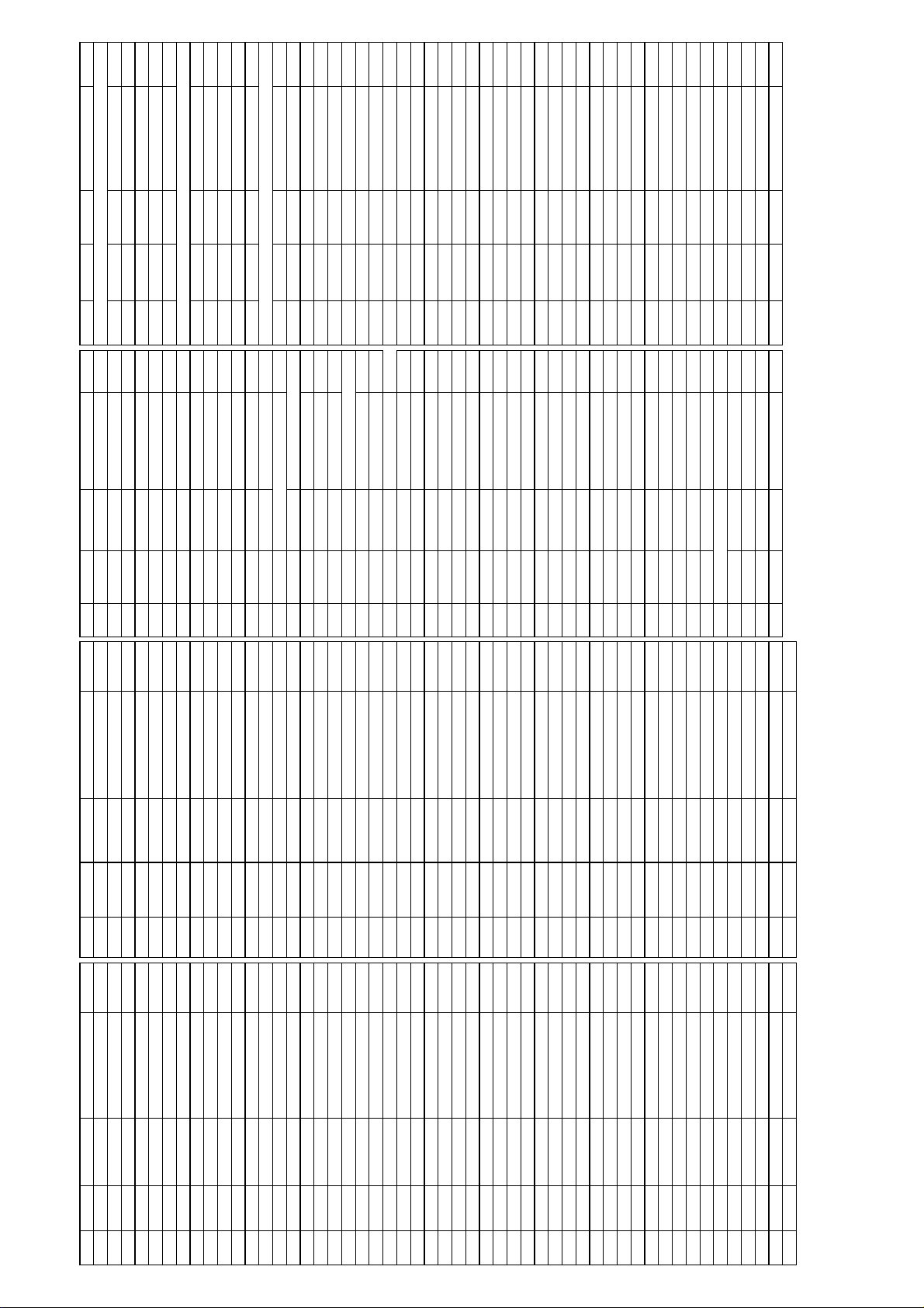
RF Unit/VC0 Unit/Mechanica1 Parts/PTT Unit/Be1t C1ip/Packing/Charge Unit
Ref.No.
Parts No.
Description
Parts Name
Ver.
Ref.No.
Parts No.
Description
Parts Name
Ver.
Ref.No.
Parts No.
Description
Parts Name
Ver.
Ref.No.
Parts No.
Description
Parts Name
Ver.
R144
RK3050
Chip R
ERJ3GSY3103V
R205
RK3030
Chip R
ERJ3GSYJ221V
R301
RK3026
Chip R
ERJ3GSYJ101V
PTT Unit
R145
RK3074
Chip R
ERJ3GSYJ105V
R206
RK3059
Chip R
ERJ3GSYJ563V
R302
RK3030
Chip R
ERJ3GSYJ221V
SW401
UU0026
Switch
EVQPLBA0S
R146
RK3074
Chip R
ERJ3GSYJ105V
R209
RK3026
Chip R
ERJ3GSYJ101V
R303
RK3050
Chip R
ERJ3GSYJ103V
SW402
UU0018
Switch
S0P-110HST
R147
RK3074
Chip R
ERJ3GSYJ105V
R210
RK3001
Chip R
ERJ3GSY0R00V
R304
RK3062
Chip R
ERJ3GSYJ104V
SW403
UU0018
Switch
S0P-111HST
R148
RK3060
Chip R
ERJ3GSYJ683V
R211
RK3062
Chip R
ERJ3GSYJ104V
R305
RK3062
Chip R
ERJ3GSYJ104V
SW404
UU0018
Switch
S0P-112HST
R149
RK3074
Chip R
ERJ3GSYJ105V
R212
RK3001
Chip R
ERJ3GSY0R00V
R306
RK3062
Chip R
ERJ3GSYJ104V
R150
RK3034
Chip R
ERJ3GSYJ47lV
R213
RK3050
Chip R
ERJ3GSYJ103V
R307
RK3052
Chip R
ERJ3CSYJ153V
Belt clip
R153
RK3054
Chip R
ERJ3GSYJ223V
R214
RK3050
Chip R
ERJ3GSYJ103V
R308
RK3042
Chip R
ERJ3GSYJ222V
AA0020
Screw
TH M2.6+4 Fe/2pcs
R154
RK3042
Chip R
ERJ3GSYJ222V
R215
RK3059
Chip R
ERJ3GSYJ563V
R309
RK3050
Chip R
ERJ3GSYJl03V
BB0009Y
Hand Strap DJS4l
R155
RK3058
Chip R
ERJ3GSYJ473V
R216
RK3062
Chip R
ERJ3GSYJ104V
R310
RK3037
Chip R
ERJ3GSYJ821V
BH0008A
Belt Clip DJK1
R156
RK3041
Chip R
ERJ3GSYJ182V
R219
RK3058
Chip R
ERJ3GSYJ473V
R311
RK3042
Chip R
ERJ3GSYJ222V
HP0003
Protect.Bag
5x75x110
R157
RK3041
Chip R
ERJ3GSYJ182V
R220
RK3026
Chip R
ERJ3GSYJ101V
TS0097Y
Case
VC0 Case
YZ0121
Tape
20mm
R158
RK3059
Chip R
ERJ3GSYJ563V
R221
RK3038
Chip R
ERJ3GSYJ102V
UT0030
Terminal
0.6Pin
Packing
R159
RK3047
Chip R
ERJ3GSYJ562V
TC101
CT0012
Trinner
CTZ10AV
Mechanical Parts
HK0402A
Package
DJl90
R160
RK3054
Chip R
ERJ3GSYJ223V
X101
XQ0076
Crystal
HC-49U 21.25MHZ
AB0012
Screw
PH/S MZ. 6+5 Fe/2pcs
HM0153A
Carton Box
10PCS DJG5T
R161
RK3052
Chip R
ERJ3GSYJ153V
X102
XK0003
Crystal
CDBX450C7
AF0020
Screw
0PH M2+3 Fe/6pcs
HP0031
Protec.Bag
5x100x200
R162
RK3052
Chip R
ERJ3GSYJ153V
XF101
XF0022
Filter
UM-1 21.7MHZ
AK0001
Screw
P0X BZ+4 FE/5pcs
HU0094
P.MTL/Carton DJG5T
R163
RK3030
Chip R
ERJ3GSYJ221V
XF102
XF0022
Filter
UM-1 21.7MHZ
AN0012
Scrcv
NUT N7X0.75 BR/B
HU0095
1nter Ni-Cd Large
R164
RK3058
Chip R
ERJ3GSYJ473V
FG0212
Cushion DJ190
AX0003
Screw
0PH P2+16 FeAB/4pcs
HU0097
1nter 10pcs. DJG5T
R166
RK3046
Chip R
ERJ3GSYJ472V
FG0215
Cushion DJ191
DP0105
LCD Panel DJ190
PH0009A
GUA Card
Warranty Cert T
R167
RK3038
Chip R
ERJ3GSYJ102V
TS0101Y
Shad Case
PM shield
DS0364B
Label
Serial No
T
PT0004A
Scrial No.
For Carton/2pcs
R168
RK0105
Chip R
ERJ3GSYJ2R2V
UP0292D
PCB
DS0388
Label
Serial No
PK0057
Schematic Diagram
R169
RK3032
Chip R
ERJ3GSYJ331V
VCO Unit
FG0180Y
Ruber
DC Cap DJG5
PS0227B
Manual
1nstruction DJ190T
R170
RK3038
Chip R
ERJ3GSYJ102V
C301
CU3035
Chip C
C1608JB1H102KTA
FG0181Y
Ruber
Dial Ruber DJ190
EA57
Antenna
VHF L
R171
RK3058
Chip R
ERJ3GSYJ473V
C302
CS0377
Chip Tantal
TMCMB0G476MTR
FG0186Y
Ruber
Jack Rubber DJ190
EA58
Antenna
VHF F
R172
RK3054
Chip R
ERJ3GSYJ223V
C303
CU3047
Chip C
C1608JB1H103KTA
FG0187Y
Ruber
Jack CapDJ190
EBP36
Battery
Ni-Cd Battery Pack
R173
RK3044
Chip R
ERJ3GSYJ332V
C304
CU3037
Chip C
C1608JB1H103KTA
FG0189Y
Rubcr
PTT Ruber DJ190
EBP37
Battery
Ni-Cd Battery Pack
R174
RK3071
Chip R
ERJ3GSYJ564V
C305
CU3031
Chip C
C1608JB1H471KTA
FG0234Y
Ruber
MIC Holder DJ190
EDC63
Chager
R175
RK3054
Chip R
ERJ3GSYJ223V
C306
CU3006
Chip C
C1608CH1r1050CTA
NK0042Y
Knob
V0L Knob
EDC64
Chager
R176
RK3046
Chip R
ERJ3GSYJ472V
C307
CU3035
Chip C
C1608JB1H102KTA
PR0237
Laber
FCC Partl5
T
Charge
R177
RK3070
Chip R
ERJ3GSYJ474V
C308
CU3006
Chip C
C1608CH1t1050CTA
PR0309
Laber
CE-Mark Label
E
C801
CU3031
Chip C
C1608JB1H471KTA
R178
RK3041
Chip R
ERJ3GSYJ182V
C309
CU3003
Chip C
C1608CH1t1020CTA
TS0103Y
RF Shield
D801
XD0294
Diode
U2FWJ44N(TE12R)
R179
RK3056
Chip R
ERJ3GSYJ333V
C310
CU3031
Chip C
C1608JB1H471KTA
YZ0149
Tape
LCD Tape DJG5
D802
XD0294
Diode
U2FWJ44N(TE12R)
R180
RK3042
Chip R
ERJ3GSYJ222V
C311
CU3035
Chip C
C1608JB1H102KTA
KB0059Y
Rear Case
DJ190
D803
XD0290
Diode
MA111-TX
R181
RK3046
Chip R
ERJ3GSYJ472V
C312
CU3035
Chip C
C1608JB1H102KTA
UE0029A
Conncctor
BNC CH7031B
D804
XD0261
Diode
S3DG7
R182
RK3058
Chip R
ERJ3GSYJ473V
C313
CU3035
Chip C
C1608JB1H102KTA
AX0001
Screw
0PH P2+4 Fens/3pcs
D805
XD0130
Diode
DA204U T106
R183
RK3042
Chip R
ERJ3GSYJ222V
C314
CU3026
Chip C
C1608CH1H181JT-AS
ES0011BZ
Speaker
SP.036M9014
Q801
XT0088
Transistor
2SA1213Y TE12R
R184
RK3055
Chip R
ERJ3GSYJ273V
D301
XD0299
Diode
MA304-TX
FG0188
Ruber
Front Key DJ190
R801
RK0003
Chip R
2125 1/10 15ohn
R185
RK3062
Chip R
ERJ3GSYJ104V
D302
XD0293
Diode
1SV257(TPH3)
FG0190Y
0N-A1R DJ190
R802
RK3046
Chip R
1608 1/16 4.7 kohm
R186
RK3046
Chip R
ERJ3GSYJ472V
D303
XD0129
Diode
1SS318 TT11
FG0210Z
Speaker Custlion
JK801
UJ0015
Connector
HEC2781 010020
R187
RK3058
Chip R
ERJ3GSYJ473V
D304
XD0299
Diode
MA304-TX
KZ0072Y
Case Assy
Front Case DJ190
MBCK07AA
Wire
#28 02-70-02
R188
RK3050
Chip R
ERJ3GSYJ103V
L301
QA0120
Coil
QA0120
ST0052Y
Holder
SP Filture DJG5
MBCK07AA
Wire
#28R02-70-02
R189
RK3050
Chip R
ERJ3GSYJ103V
L301
QA0077A
Coil
QA077A
TA2
UX1035
Wire
DJ180 W201
QB0020
Coil
H5DT6X1.5X3
R191
RK3050
Chip R
ERJ3GSYJ3103
L302
QC0442
Coil
MLF1608A1R0K-T
AF0020Z
Screw
0PH M2+3 Fe/3pcs
TT3007
Tube
6.0x10mm
R192
RK3014
Chip R
ERJ3GSYJ100V
?
L303
QKA65A
Coil
KRl.5 3.5T 0.4
AX0001
Screw
0PH P2+4 Fe/3pcs
R193
RK3038
Chip R
ERJ3GSYJ102V
L304
QC0454
Coil
MLF1608K100K-T
FP0093AY
Teaminal Frame
R195
RK3056
Chip R
ERJ3GSYJ333V
L305
QC0454
Coil
MLF1608K100K-T
FP0094Y
Release Knob
R196
RK3052
Chip R
ERJ3GSYJ153V
Q301
XT0137
Transistor
2SC5065-O(TE85L)
SC0008A
Spring
Release DJG5
R198
RK3043
Chip R
ERJ3GSYJ272V
Q302
XT0137
Transistor
2SC5065-O(TE85L)
SD0045
Spring
Team. DJF5/3pcs
R203
RK3038
Chip R
ERJ3GSYJ102V
Q303
XU0131
Transistor
DTC114EUA T106
TS0100
Shield
R204
RK3030
Chip R
ERJ3GSYJ221V
Page 20
E,T,TA
E,TA,TAH
TFH
TAH
T,E.,TA
T
E,TA,TAH
T.E.TA.TAH
Page 20

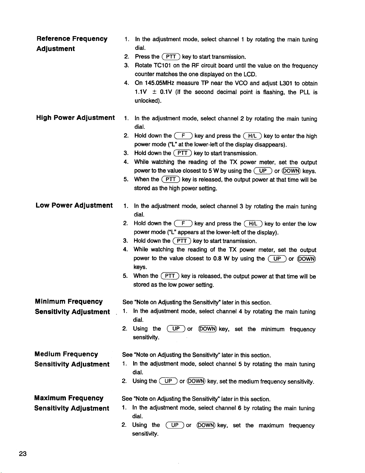
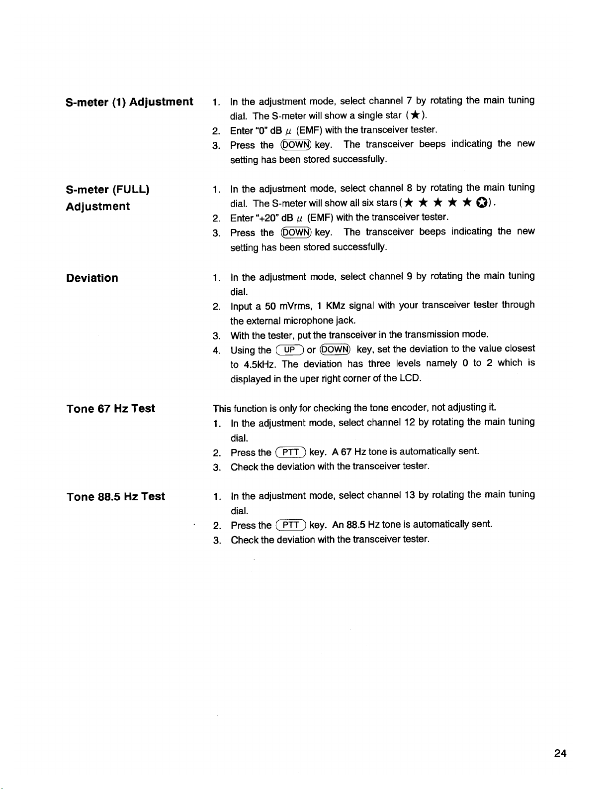
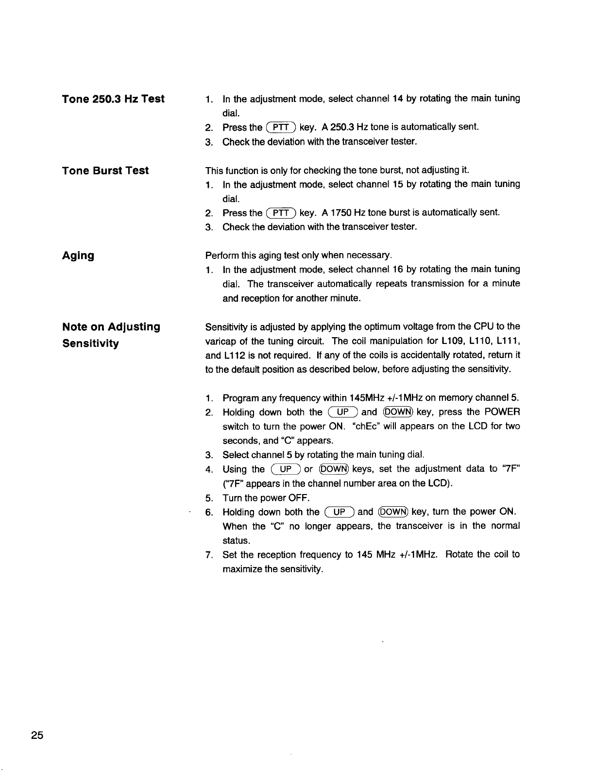
ADJUSTMENT
1) Required Test Equipment
The following items are required to adjust radio parameters:
1. Regulated power
Supply voltage:5 ~ 14 VDC
supply
Current : 3 A or more
2. Digital multi meter
Voltage range : FS = Approx. 20 V
Current:10A or more
Input resistance : High impedance
3. Oscilloscope
Measurable frequency : Audio frequency
4. Audio dummy load
Impedance: 8 ohm
Dissipation: 1 W or more
Jack:3.5 mm D
5. SSG
Output frequency:200 MHz or more
Output level : -20 dB/0.1 a V ~ 120dB/1V
Modulation : AM/FM
6. Spectrum Analyzer
Measuring range : Up to 2 GHz or more
7. Power meter
Measurable frequency:Up to 200 MHz
Impedance : 50 ohm unbalanced
Measuring range : 0.1W ~ 10 W
Measurable frequency : Up to 100 kHz
8. Audio voltmeter
Sensitivity : 1 mV to 10 V
Output frequency : 67 Hz to 10 kHz
9. Audio generator
Output impedance : 600 ohm , unbalanced
Measurable frequency : 1 kHz
10. Distortion meter
Input level : Up to 40 dB
/SINAD meter
Distortion level : 1 % - 100%
Measurable frequency : Up to 200 MHz
11. Frequency counter
Measurable stability : Approx. +/-0. 1 ppm
Measurable frequency : Up to 200 MHz
12. Linear detector
Characteristics: Flat
CN:60 dB or more
Note
* Standard modulation:
1 kHz +/-3.5 kHz/DEV
* Reference sensitivity:
12dBSINAD
*Specified audio output level : 200 mW at 8 ohm
*Standard audio output level : 50 mW at 8 ohm
*Use an RF cable (3D2W: 1 m) for test equipment.
*Attach a fuse to the RF test equipment.
*All SSG outputs are indicated by EMF.
* Supply voltage for the transceiver: 13.8 VDC
Page-21
Page 21

Page 22
Page 23
Page 24
Page 25
Page 26

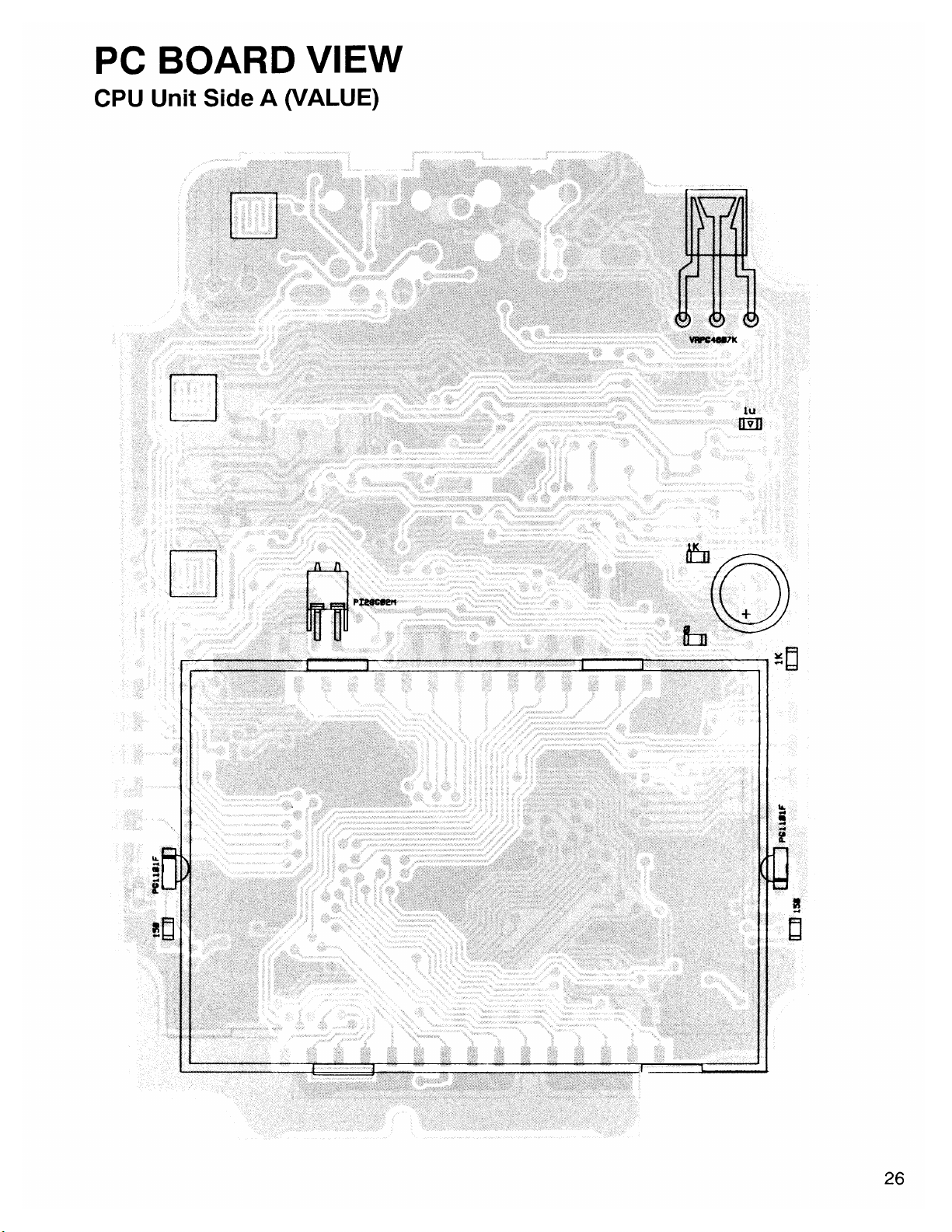
CN4
D10
L10
R1006
R1013
D1
R1
LCD1
R1007
D3
R3
Page 27

Page 28

Page 29

Page 30

Page 31

Page 32

SW402
SW404
SW401
SW403
Page 33

Page 34

R802
D801
D804
D805
R801
Q801
D803
D802
Page 35

Page 36
Page 37
Page 38
Page 39

Page 40

Page 41

 Loading...