

Page 1
DR-135/435FX
S e r v i c e M a n u a l
C O N T E N T S
SPECIFICATIONS
GENERAL
TRANSMITTER..........................................
RECEIVER
CIRCUIT D ISC RE TION
1) Receiver System DR-135..............................
2) Transmitter System DR-135
3) PLL Synthesizer Circuit DR-135
4) Receiver System DR-435
5) Transmitter System DR-435
6) PLL Synthesizer Circuit DR-435.............
7) CPU and Peripheral Circuit
8) Power Supply Circuit
9) M38268MCA075GP (XA1130)
SEMICON DUC TOR DATA
1) NJM7808FA(XA0102)
2) TC4S66F (XA0115)
3) AN8010M (XA0119).....
4) TC4W53FU(XA0348)
5) TA31136FN (XA0404)
6) LA4425A (XA0410)........................................
7) BR24L32FJ (XA0604Z)
8) S-80845ALMP (XA0620)
9) S-816A50AMC (XA0925)
10) NJM78M05DL1 A(XA0947)
11) LM2904PWR (XA1103)...
12) LM2902PWR (XA1106)..................................
13) MB15E07SR (XA1107)...................................
14) RA60H1317M1 (XA1108)
15) S-AU82L (XA1142).........................................
16) Transistor, Diode and LED Outline Drawing...
17) LCD Connection (TTR3626UPFDHN)
EXPLO DED VIEW
1) Top and Front View........................................
2) Bottom View...................................................
3) LCD Assembly.................................
......................................................
.............................
....................................
...... .......
.......
....................
........
.................
......................
..........................
.......... .........
..............................
...........
...... .....
........ .......
................................
.....................
........
...............................
...................
.......
..............................
...............
.. ......
.......................
...........
.
........
................
......................
.........
.
.............
PARTS LIST
2
2
2
3,4
4
4,5
5,6
6,7
7
8
8
9-11
CPU Unit................................................. 24
MAIN Unit DR-135
MAIN Unit DR-435.
Mechanical Parts.........
Packing Parts
ACCESSORIES.......;.......................... 31
ACCESSORIES (SCREW SET)
............................ 24-27
....
........................... 27-30
........................
........................................
............
30
31
31
DR-135 ADJUSTMENT
1) Adjustment Spot
2) VCO and RX Adjustment Specification.. 33
3) TX Adjustment Specification
4) RX Test Specification............................ 34
5) TX Test Specification............................ 35
.............................
.................
.....
32
33
DR-435 ADJUSTMENT
12
12
12
12
.
13
13
14
14
14
14
15
15
16
17
18
19
20
21
22
23
1) Adjustment Spot
2) VCO and RX Adjustment Specification.. 37
3) TX Adjustment Specification
4) RX Test Specification
5) TX Test Specification... ...
PC BOARD VIEW
1) CPU Unit Side A DR-135 (UP0538A).... 41
2) CPU Unit Side B DR-135 (UP0538A).... 41
3) CPU Unit Side ADR-435 (UP0545)
4) CPU Unit Side B DR-435 (UP0545)...... 42
5) MAIN Unit Side A DR-135 (UP0538A)... 43
6) MAIN Unit Side B DR-135 (UP0538A).. 43
7) MAIN Unit Side A DR-435 (UP0545)..... 44
8) MAIN Unit Side B DR-435 (UP0545).... 44
SCHEMATIC DIAGRAM
1) CPU Unit DR-135
2) CPU Unit DR-435
3) MAIN Unit DR-135
4) MAIN Unit DR-435
................................... 36
............ . 38
........
................... 39
....................
.....,......
.............
..................
................................ 48
....................
....................
.............
......
40
42
45
46
47
BLOCK DIAGRAM
1) DR-135................................................. 49
2) DR-435................................................. 50
A L I N G O, inc
Page 2
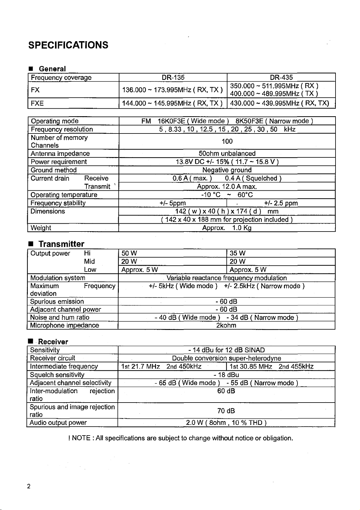
SPE C I F I C ATI ON S
■ General
Frequency coverage DR-135 DR-435
FX
FXE
Operating mode FM 16K0F3E ( Wide mode ) 8K50F3E ( Narrow mode )
Frequency resolution 5 , 8.33 , 10 , 12.5 , 15 , 20 , 25 , 30 , 50 kHz
Number of memory
Channels
Antenna impedance
Power requirement 13.8V DC +/-15% ( 11.7 - 15.8 V )
Ground method Negative ground
Current drain Receive
Transmit
Operating temperature
Frequency stability
Dimensions 142 ( w ) x 40 ( h ) x 174 ( d ) mm
Weight
136.000 - 173.995MHz ( RX, TX )
144.000 - 145.995MHz ( RX, TX )
50ohm unbalanced
0.6 A (max.) 0.4 A ( Squelched )
Approx. 12.0 A max.
-10 °C - 60°C
+/- 5ppm
( 142 x 40 x 188 mm for projection included )
Approx. 1.0 Kg
350.000 ~ 511.995MHz ( RX )
400.000 ~ 489.995MHz ( TX )
430.000 - 439.995MHz ( RX, TX)
100
+/- 2.5 ppm
■ Transmitter
Output power Hi
Mid
Low
Modulation system
Maximum Frequency
deviation
Spurious emission
Adjacent channel power
Noise and hum ratio
Microphone impedance 2kohm
■ Receiver
Sensitivity -14 dBu for 12 dB SINAD
Receiver circuit
Intermediate frequency
Squelch sensitivity
Adjacent channel selectivity
Inter-modulation rejection
ratio
Spurious and image rejection
ratio
Audio output power
50 W 35 W
20 W 20 W
Approx. 5 W Approx. 5 W
Variable reactance frequency modulation
+/- 5kHz ( Wide mode ) +/- 2.5kHz ( Narrow mode )
-60 dB
- 60 dB
- 40 dB ( Wide mode ) - 34 dB ( Narrow mode )
Double conversion super-heterodyne
1st 21.7 MHz 2nd 450kHz
- 65 dB ( Wide mode ) - 55 dB ( Narrow mode )
2.0 W ( 8ohm , 10 %THD)
1st 30.85 MHz 2nd 455kHz
- 18 dBu
60 dB
70 dB
! NOTE : All specifications are subject to change without notice or obligation.
2
Page 3
C IR C U I T D E S C R I P T IO N
1) Receiver System DR-135
The receiver system is a double super-heterodyne system with a 21.7MHz first IF and a 450kHz
second IF.
1. Front End
2. IF Circuit
3. Demodulation Circuit
The received signal at any frequency in the 136.000MHz to 173.995MHz
range is passed through the low-pass filter (L116, L115, L114, L113, C204,
C203, C202, C216 and C215) and tuning circuit {L105, L104 and D105,
D104), and amplified by the RF amplifier (Q107). The signal from Q107 is
then passed through the tuning circuit (L103, L102, and variable capacitor
D103, D102) and converted into 21.7MHz by the mixer (Q106). The tuning
circuit, which consists of L105, L104, variable capacitor D105 and D104,
L103, L102, variable capacitor D103 and D102, is controlled by the
tracking voltage from the VCO. The local signal from the VCO is passed
through the buffer (Q145), and supplied to the source of the mixer (Q106).
The radio uses the lower side of the super-heterodyne system.
The mixer mixes the received signal with the local signal to obtain the sum
of and difference between them. The crystal filter (XF102, XF101) selects
21.7 MHz frequency from the results and eliminates the signal of the
unwanted frequencies. The first IF amplifier (Q105) then amplifies the
signal of the selected frequency.
After the signal is amplified by the first IF amplifier (Q105), it is input to
pin16 of the demodulator IC (IC108). The second local signal of 21.25MHz
{shared with PLL IC reference oscillation), which is oscillated the external
oscillator X601 and IC601, is input through pin 1 of IC108. Then, these
two signals are mixed by the internal mixer in IC108 and the result is
converted into the second IF signal with a frequency of 450kHz. The
second IF signal is output from pin 3 of IC108 to the ceramic filter (FL102
or FL101), where the unwanted frequency band of that signal is
eliminated, and the resulting signal is sent back to the IC108 through pin
5. The second IF signal input via pin 5 is demodulated by the internal
limiter amplifier and quadrature detection circuit in IC 108, and output as
an audio signal through pin 9.
4. Audio Circuit
The audio signal from pin 9 of IC 108 is amplified by the audio amplifier
(1C120:A), and switched by the signal switch IC (IC111) and then input it to
the de-emphasis circuit.
And is compensated to the audio frequency characteristics in the
de-emphasis circuit (R203, R207, R213, R209, C191, C218, C217) and
amplified by the AF amplifier (IC120:B). The signal is then input to volume
(VR1). The adjusted signal is sent to the audio power amplifier (IC117)
through the pin 1 to drive the speaker.
3
Page 4
5. Squelch Circuit
The detected output which is outputted from pin 9 of IC108 is inputted to
pin 8 of IC108 after it was been amplified IC120:Aand it is outputted from
pin 7 after the noise component was been eliminated from the composed
band pass filter in the built in amplifier of the IC, then the signal is rectified
by the internal diode in IC108 to convert into DC component. The adjusted
voltage level at VR101 is delivered to the comparator of the CPU.
The voltage is led to pin 2 of CPU and compared with the setting voltage.
The squelch will open if the input voltage is lower than the setting voltage.
During open squelch, pin 30 (SQC) of the CPU becomes “L” level, AF
control signal is begin controlled and sounds is outputted from speaker.
6. WIDE/NARROW
Switching circuit secor|d IF 450kHz signal which passes through filter FL101 (wide)
and FL102 (narrow) during narrow, changes its width using the width
control switching D116 and D115.
2) Transmitter System DR-135
1. Modulator Circuit
The audio signal is converted to an electrical signal by the microphone,
and input it to the microphone amplifier (Q6). Amplified signal which
passes through mic-mute control IC109 is adjusted to an appropriate
mic-volume by means of mic-gain adjust VR106.
IC114:D and C consists of two operational amplifiers; one amplifier (pin
12,13 and 14) is composed of pre-emphasis and I DC circuit and the other
(pin 8, 9 and 10) is composed of a splatter filter. The maximum frequency
deviation is obtained by VR107. And input to the signal switch (IC113)
{9600 bps packet signal input switch) and input to the cathode of the
variable capacitor of the VCO, to change the electric capacity in the
oscillation circuit. This produces the frequency modulation.
2. Power Amplifier Circuit
The transmitted signal is oscillated by the VCO, amplified by the younger
amplifier {Q115), and input to the final power module (IC110). The signal is
then amplified by the final power module (IC110) and led to the antenna
switch (D110) and low-pass filter (L113, L114, L115, L116, C215, C216,
C202, C203 and C204), where unwanted high harmonic waves are
reduced as needed, and the resulting signal is supplied to the antenna.
3. APC Circuit
Part of the transmission power from the low-pass filter is detected by
D111, converted to DC. The detection voltage is passed through the APC
circuit (!C114:A, IC114:B), then it controls the APC voltage supplied to
final power module IC110 to fix the transmission power.
3) PLL Synthesizer Circuit DR-135
1.PLL
The dividing ratio is obtained by sending data from CPU (IC1) to pin 10
and sending clock pulses to pin 9 of the PLL IC (IC116). The oscillated
signal from the VCO is amplified by the buffer (Q134 and Q135) and input
to pin 8 of IC116. Each programmable divider in IC116 divides the
frequency of the input signal by N according to the frequency data, to
generate a comparison frequency of 5 or 6.25 kHz.
4
Page 5
2. Reference Frequency
Circuit "^e re^erence frequency appropriate for the channel steps is obtained by
dividing the 21.25 MHz reference oscillation (X102) by 4250 or 3400,
according to the data from the CPU (IC1). When the resulting frequency is
5 kHz, channel step of 5,10,15, 20, 25, 30 and 50 kHz are used. When it
is 6.25 kHz, the 12.5 kHz channel step is used.
3. Phase Comparator Circuit
4. PLL Loop Filter Circuit
5. VCO Circuit
6. VCO Shift Circuit
The PLL (IC116) uses the reference frequency, 5 or 6.25 kHz. The phase
comparator In the IC116 compares the phase of the frequency from the
VCO with that of the comparison frequency, 5 or 6.25 kHz, which is
obtained by the internal divider in IC116.
If a phase difference is found in the phase comparison between the
reference frequency and the VCO output frequency, the charge pump
output (pin 5) of IC116 generates a pulse signal, which is converted DC
voltage by the PLL loop filter and input to the input to the variable
capacitor of the VCO unit for oscillation frequency control.
A Colpitts oscillation circuit driven by Q131 directly oscillates the desired
frequency. The frequency control voltage determine in the CPU (IC1) and
PLL circuit is input to the variable capacitor (D122 and D123). This change
the oscillation frequency, which is amplified by the VCO buffer (Q134,
Q145) and output from the VCO area.
During transmission or the AIR band Reception (118-136 MHz), the VCO
shift circuit turns ON Q138, change control the capacitance of L123 and
safely oscillates the VCO by means of H signal from pin 42 of 1C1.
4) Receiver System DR- 435
The receiver system is a double super-heterodyne system with a 30.85MHz first IF and a 455kHz
second IF.
1. Front End
2. IF Circuit
The received signal at any frequency in the 430.000MHz to 439.995MHz
range is passed through the low-pass filter ( L115, L114, L116, C204,
C203, C202, C216 and C215) and amplified by the RF amplifier (Q107).
The signal from Q107 is then passed through the BPF circuit (L103, L102)
and converted into 30.85MHz by the mixer (Q106). The local signal from
the VCO is passed through the buffer (Q134, Q145), and supplied to the
source of the mixer (Q106). The radio uses the tower side of the
super-heterodyne system.
The mixer mixes the received signal with the local signal to obtain the sum
of and difference between them. The crystal filter (XF101) selects 30.85
MHz frequency from the results and eliminates the signal of the unwanted
frequencies. The first IF amplifier (Q105) then amplifies the signal of the
selected frequency.
5
Page 6
3. Demodulation Circuit
After the signal is amplified by the first IF amplifier (Q105), it is input to
pin16 of the demodulator IC (IC108). The second local signal of
30.395MHz (Crystal oscillator) is input through pin 1 of IC108. Then, these
two signals are mixed by the internal mixer in IC108 and the result is
converted into the second IF signal with a frequency of 455kHz. The
second IF signal is output from pin 3 of IC108 to the ceramic filter (FL101
or FL102), where the unwanted frequency band of that signal is
eliminated, and the resulting signal is sent back to the IC108 through pin
5.
The second IF signal input via pin 5 is demodulated by the internal limiter
amplifier and quadrature detection circuit in IC 108, and output as an
audio signal through pin 9.
4. Audio Circuit
The audio signal from pin 9 of IC 108 is amplified by the audio amplifier
(IC120:A), and switched by the signal switch IC (IC111) and then input it to
the de-emphasis circuit.
And is compensated to the audio frequency characteristics in the
de-emphasis circuit (R203, R207, R213, R209, C191, C218, C217) and
amplified by the AF amplifier (IC120:B). The signal is then input to volume
(VR1). The adjusted signal is sent to the audio power amplifier (IC117)
through the pin 1 to drive the speaker.
5. Squelch Circuit
The detected output which is outputted from pin 9 of IC108 is inputted to
pin 8 of IC108 after it was been amplified IC120:A and it is outputted from
pin 7 after the noise component was been eliminated from the composed
band pass filter in the built in amplifier of the IC, then the signal is rectified
by the internal diode in IC108 to convert into DC component. The adjusted
voltage level at VR101 is delivered to the comparator of the CPU.
The voltage is led to pin 2 of CPU and compared with the setting voltage.
The squelch will open if the input voltage is lower than the setting voltage.
During open squelch, pin 30 (SQC) of the CPU becomes “L” level, AF
control signal is begin controlled and sounds is outputted from speaker.
6. WIDE/NARROW
Switchina circuit seconc* ^ 455kHz signal which passes through filter FL101 (wide)
and FL102 (narrow) during narrow, changes its width using the width
control switching D116 and D115.
5) Transmitter System DR- 435
1. Modulator Circuit
6
The audio signal is converted to an electrical signal by the microphone,
and input it to the microphone amplifier (Q6). Amplified signal which
passes through mic-mute control IC109 is adjusted to an appropriate
mic-volume by means of mic-gain adjust VR106.
IC114:D and C consists of two operational amplifiers; one amplifier (pin
12,13 and 14) is composed of pre-emphasis and IDC circuit and the other
(pin 8, 9 and 10) is composed of a splatter filter. The maximum frequency
deviation is obtained by VR107. And input to the signal switch (IC113)
(9600 bps packet signal input switch) and input to the cathode of the
variable capacitor of the VCO, to change the electric capacity in the
oscillation circuit. This produces the frequency modulation.
Page 7
2. Power Amplifier Circuit
The transmitted signal is oscillated by the VCO, amplified by the drive
amplifier (Q138) and younger amplifier (Q115), and input to the final
power module (IC110). The signal is then amplified by the final power
module (IC110) and led to the antenna switch (D110) and low-pass filter
(L116, L114, L115, C215, C216, C202, C203 and C204), where unwanted
high harmonic waves are reduced as needed, and the resulting signal is
supplied to the antenna.
3. APC Circuit
Part of the transmission power from the low-pass filter is detected by
D111, converted to DC. The detection voltage is passed through the APC
circuit (IC114:A, IC114:B), then it controls the APC voltage supplied to the
final power module IC110tofix the transmission power.
6) PLL Synthesizer Circuit DR- 435
1. PLL
2. Reference Frequency
Circuit "^e reference frequency appropriate for the channel steps is obtained by
The dividing ratio is obtained by sending data from CPU (IC1) to pin 10
and sending clock pulses to pin 9 of the PLL IC (IC116). The oscillated
signal from the VCO is amplified by the buffer (Q134 and Q135) and
input to pin 8 of IC116, Each programmable divider in IC116 divides the
frequency of the input signal by N according to the frequency data, to
generate a comparison frequency of 5 or 6.25 kHz.
dividing the 21.25 MHz reference oscillation (X102) by 4250 or 3400,
according to the data from the CPU (IC1). When the resulting frequency
is 5 kHz, channel step of 5, 10, 15, 20, 25, 30 and 50 kHz are used.
When it is 6.25 kHz, the 12.5 kHz channel step is used.
3. Phase Comparator Circuit
4. PLL Loop Filter Circuit
5. VCO Circuit
The PLL (IC116) uses the reference frequency, 5 or 6.25 kHz. The phase
comparator in the IC116 compares the phase of the frequency from the
VCO with that of the comparison frequency, 5 or 6.25 kHz, which is
obtained by the internal divider in IC116.
If a phase difference is found in the phase comparison between the
reference frequency and the VCO output frequency, the charge pump
output (pin 5) of IC116 generates a pulse signal, which is converted DC
voltage by the PLL (oop filter and input to the input to the variable
capacitor of the VCO unit for oscillation frequency control.
A Colpitts oscillation circuit driven by Q131 directly oscillates the desired
frequency. The frequency control voltage determine in the CPU (IC1) and
PLL circuit is input to the variable capacitor (D122 and D123). This
change the oscillation frequency, which is amplified by the VCO buffer
(Q134, Q145) and output from the VCO unit.
7
Page 8
7) CPU and Peripheral Circuits
1. LCD Display Circuit
2. Reset and Backup
3. S (Signal) Meter Circuit
4. DTMF Encoder
5. Tone Encoder
The CPU turns ON the LCD via segment and common terminals with 1/4
the duty and 1/3 the bias, at the frame frequency is 64 Hz.
When the power from the DC cable increases from Circuits 0 V to 2.5 V or
more, “H” level reset signal is output from the reset IC (IC4) to pin 33 of
the CPU (IC1), causing the CPU to reset. The reset signal , however,
waits at 100, and dose not enter the CPU until the CPU clock (X1) has
stabilized.
The DC potential of IF IC is input to pin 1 of the CPU (IC1), converted from
an analog to a digital signal, and displayed as the S-meter signal on the
LCD.
The CPU (IC1) is equipped with an internal DTMF encoder. The DTMF
signal is output from pin 10, through R35, R34 and R261 (for level
adjustment), and then through the microphone amplifier (IC114:A), and is
sent to the variable capacitor of the VCO for modulation. At the same time,
the monitoring tone passes through the AF circuit and is output from the
speaker.
The CPU (IC1) is equipped with an internal tone encoder. The tone signal
(67.0 to 250.3 Hz) is output from pin 9 of CPU to the variable capacitor
(D122 and D123) of the VCO for modulation.
6. DCS Encoder
The CPU (IC1) is equipped with an internal DCS code encoder. The code
(023 to 754) is output from pin 9 of CPU to the voltage control pin of
VCTCXO (X102) of the PLL reference oscillator. When DCS is ON, DCS
MUTE circuit (Q126-ON, Q133-ON, Q132-OFF) works. The modulation
activates in X102 side only.
7. CTCSS, DCS Decoder
The voice band of the AF output signal from pin 1 of IC120:A is cut by
sharp active filter IC104:A, B and C (VCVS) and amplified, then led to pin
4 of CPU. The input signal is compared with the programmed tone
frequency code in the CPU. The squelch will open when they match.
During DCS, Q108 is ON, C419 is working and cut off frequency is
lowered.
8) Power Supply Circuit
When power supply is ON, there is a “L” signal being inputted to pin 39 (PSW) of CPU which enables the CPU to
work. Then, “H” signal is outputted from pin 41 (C5C) of CPU and drives ON the power supply switch control Q8
and Q7 which turns the 5VS ON. 5VS turns ON the PLL IC (IC116), main power supply switch Q127 and Q122,
AF POWER IC117 and the 8V of AVR (IC115). During reception, pin 29 (R5) of CPU outputs “H” level, Q124 is ON,
and the reception circuits supplied by 8 V. While during transmission, pin 28 (T5) of CPU outputs “L” level which is
reverse by Q11 so that the output in Q128 will be “H” level, Q123 is ON, and the transmission circuit is supplied by
8 V. Or, in the case when the condition of PLL is UNLOCK, “H” level is outputted from pin 14 of PLL IC, UNLOCK
switch Q129 is ON, transmission switch Q128 is OFF which makes the transmission to stop.
8
Page 9
6
-o
"O
-a O Oï
ro GO
o>
\
oo GO
GO
_ "O O) —I CJI C1 W OI í> W D
í i * . \ S , 0 - t r O W N N .U l
.&» C71 Çft C/À \ \ \ O O <T>
-O -
-J -t*. —I —i <= X X ^
■ '
“D ~0 “ O "U
^ ^ ■ 0 " O T 3 T 3 C n 0 1
-------
P3
SE —i —i —i —I O Ö
3 3 - O T I 3 3 3 3 > >
------------
<T>
o
1“
O r-
cr
—ihoro
ro
ro
3> â>
>■
S z
fs?co
“U-a "0
C7)
o>
Oï
ai a>
-e*
>- >
ï>
z s: s
-pt
o>
CJl
iH U n n iu n n i n i im i
í^l [él ísi [éi [êè f¿i s fà [ä h □ [ä n n j3 r r fh @ 0 R
IH —
! —
!h —
Z i ^
HH—
M— ►
s — -
n — ►
i — -
a —
—
i
i — ►
i —
n — ►
i — -
i — ►
M— ►
1 — ►
S —
M——
1 —
! —
Hi
l l —
LIA
10
zo
HA
cia
owoo
LWÛO
zwoo
SW03
SSAV
âm
00A
093S
L93S
Z93S
S93S
fr93S
593S
993S
¿93S
893S
693S
CH93S
L193S
21D3S
î î 1 î î î 11 î î î î 11J J11JIJ J JIJ
GO GO GO CO GO CO Co GO GO GO C/0 GO GO GO C/3 GO GO CO GO GO
m m m m m m m m m m m m m m m m m m m m
O O O O O O O O Lj j O O C5 O O O O O O O O
t o c o w c o w w c o w h o r o M r o r o r o w r o h o N i - 1 - 4
* s J O ) t n ^ W N 5 - * O ( 0 C 0 ^ 0 > C J l ^ 0 i N 3 ^ O < D 0 0
-o -Tj - a “O -o
—^ o o o o
o ^ C i Ü 1 ^
~o ~o
o <z >
go ro
“0 " 0 “0 ‘0 " ü ' D _D " 0 ’D C O W C O C ^ W
oco w w wwco w w rnm m m rn
--J O CJT co
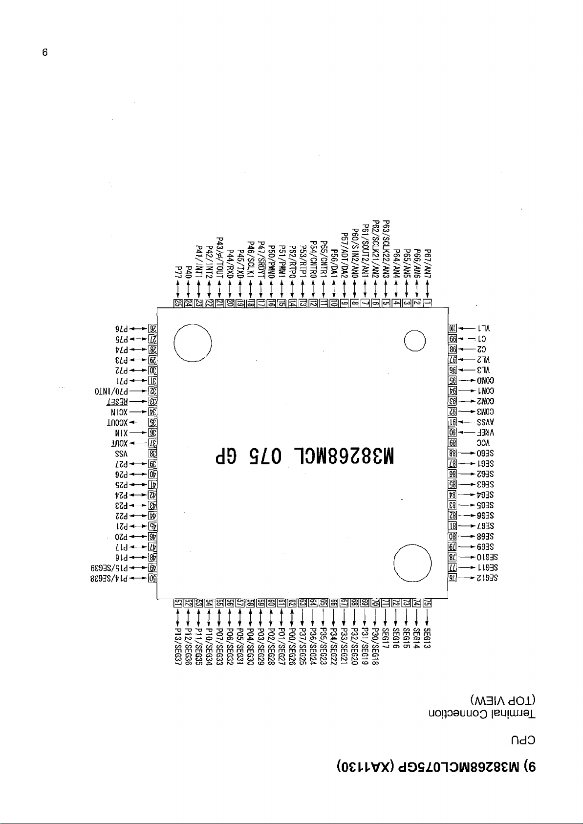
(OEWVX) d99Z(TIOIAI8928£IAI (6
(M3IA dOl)
UO IP0UUO Q |BUJLUJ0J_
ndo
Page 10
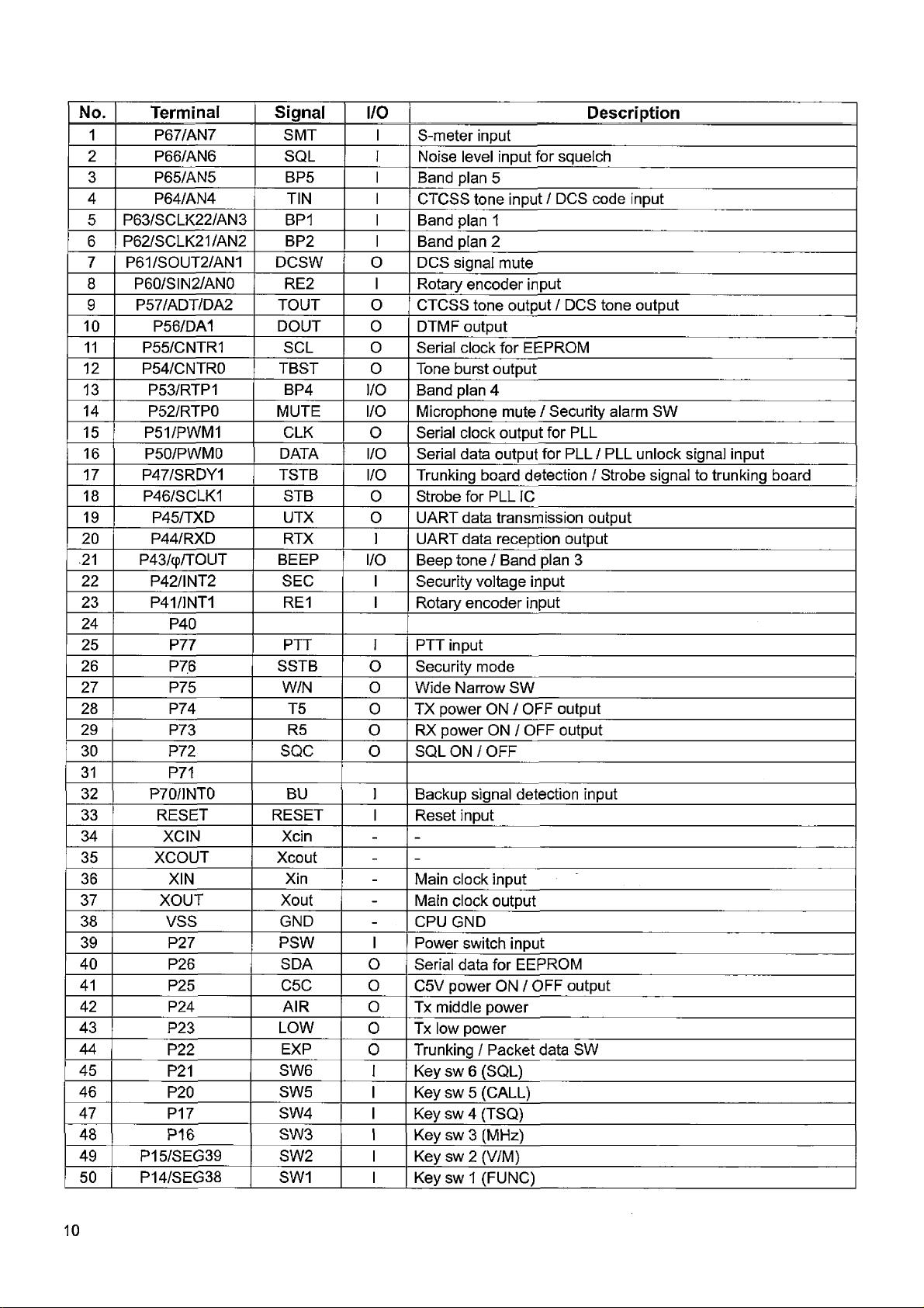
No. Terminal
1
2 P66/AN6 SQL I
3 P65/AN5 BP5 I
4
5 P63/SCLK22/AN3 BP1 I
6
7
8 P 60/S IN 2/AN 0 RE2 I
9
10
11
12 P54/CNTR0
13 P53/RTP1 BP4 I/O Band plan 4
14
15
16
17 P47/SRDY1 TSTB
18 P46/SCLK1 STB
19
20
.21 P43/(p/TOUT BEEP
22 P42/INT2 SEC I
23 P41/INT1 RE1 I
24
25
26
27
28 P74 T5
29
30
31
32 P70/INT0 BU
33 RESET RESET
34
35
36 XIN
37
38 VSS
39 P27 PSW I
40 P26 SDA o
41 P25 CSC 0
42 P24 AIR 0
43
44
45
46 P20
47 P17 SW4 I
48 P16 SW3 I
49
50
P67/AN7
P64/AN4
P62/SCLK21/AN2
P61/SOUT2/AN1
P57/ADT/DA2
P56/DA1
P55/CNTR1
P52/RTP0
P51/PWM1 CLK
P5O/PWM0
P45/TXD UTX
P44/RXD RTX
P40
P77
P76
P75
P73
P72
P71
XCIN
XCOUT
XOUT
P23
P22
P21
P15/SEG39
P14/SEG38
Signal I/O Description
SMT I
TIN I
BP2 I
DCSW 0
TOUT 0 CTCSS tone output / DCS tone output
DOUT 0 DTMF output
SCL 0 Serial clock for EEPROM
TBST 0 Tone burst output
MUTE I/O
O
DATA I/O Serial data output for PLL / PLL unlock signal input
I/O Trunking board detection / Strobe signal to trunking board
0 Strobe for PLL IC
0 UART data transmission output
I/O Beep tone / Band plan 3
PTT I
SSTB
W/N
R5
SQC
Xcin -
Xcout
Xin -
Xout
GND
LOW
EXP
SW6
SW5
SW2 I
SW1 I
o Security mode
0 Wide Narrow SW
0
o RX power ON / OFF output
o SQL O N/ OFF
0 Tx low power
0
S-meter input
Noise level input for squelch
Band plan 5
CTCSS tone input / DCS code input
Band plan 1
Band plan 2
DCS signal mute
Rotary encoder input
Microphone mute / Security alarm SW
Serial clock output for PLL
I UART data reception output
Security voltage input
Rotary encoder input
PTT input
TX power ON / OFF output
I Backup signal detection input
I Reset input
-
- -
Main clock input
-
Main clock output
-
CPU GND
Power switch input
Serial data for EEPROM
C5V power ON / OFF output
Tx middle power
Trunking / Packet data SW
I Key sw 6 (SQL)
I Key sw 5 (CALL)
Key sw 4 (TSQ)
Key sw 3 (MHz)
Key sw 2 (V/M)
Key sw 1 (FUNC)
10
Page 11
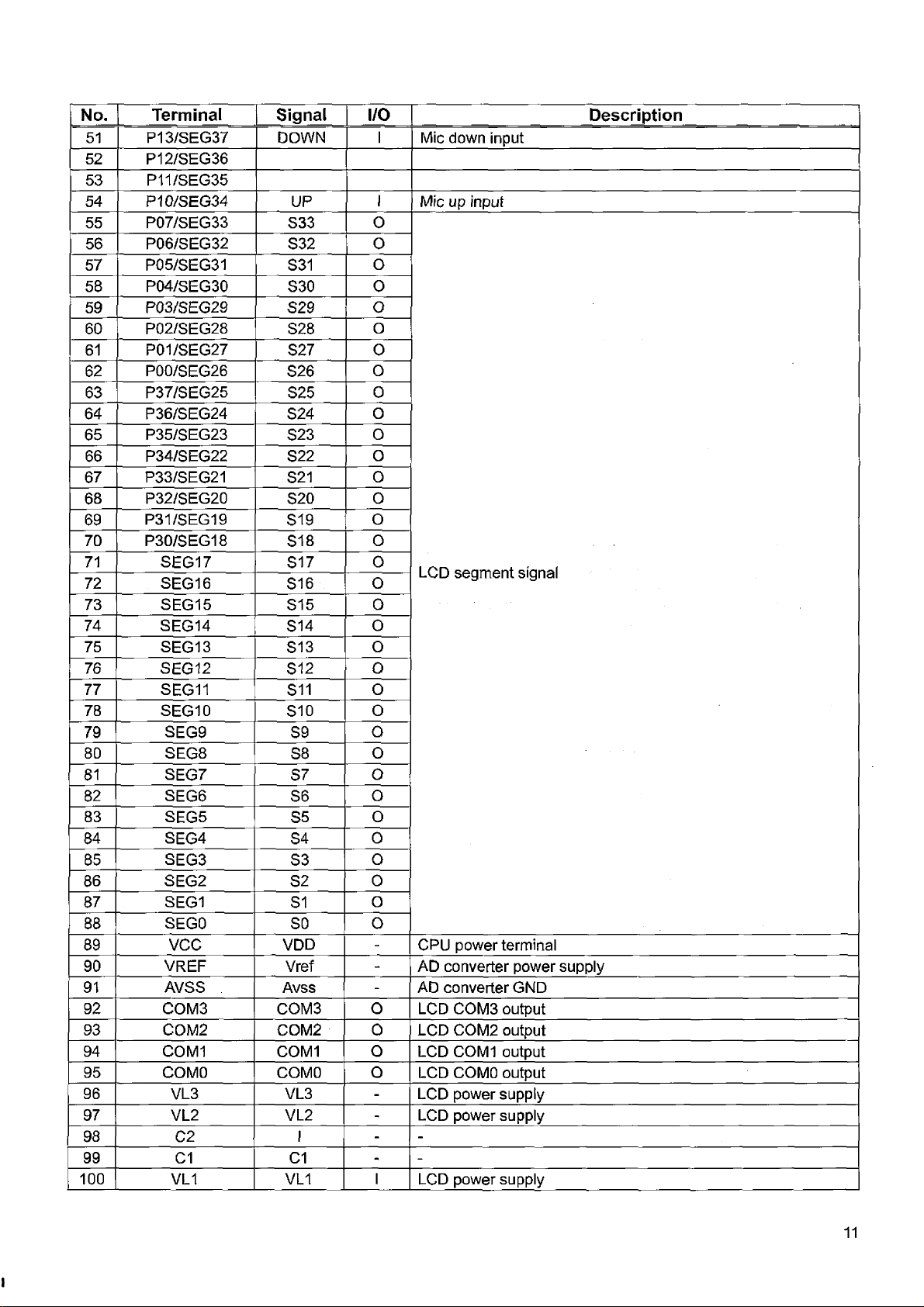
No. Terminal Signal
51
52 P 12/S EG 36
53 P11/SEG35
54
55
56
57 P05/SEG31 S31
58 P04/SEG30 S30 0
59
60
61
62
63
64
65
66 P34/SEG22
67 P33/SEG21
68 P32/SEG20 S20 0
69
70 P30/SEG18 S18 0
71 SEG17 S17 0
72 SEG16 S16 0
73 SEG15 S15 0
74 SEG14 S14 0
75 SEG13 S13 0
76
77
78 SEG10 S10 0
79 SEG9 S9
80 SEG8
81
82
83 SEG5 S5 0
84 SEG4 S4 0
85 SEG3 S3
86 SEG2 S2 0
87
88 SEGO SO o
89 VCC
90 VREF Vref
91 AVSS Avss
92 COM3 COM3 o
93 COM2 COM2 0
94 COM1 COM1 o
95 COMO COMO o
96 VL3 VL3
97 VL2 VL2
98 C2 I - -
99 C1 C1
100 VL1 VL1
P13/SEG37 DOWN I
P10/SEG34
P07/SEG33
P06/SEG32
P03ÍSEG 2Q
P02/SEG28
P01/SEG27
POO/SEG26
P37/SEG25
P36/SEG24
P35/SEG23
P31/SEG19
SEG12 S12 0
SEG11 S11
SEG7 S7 o
SEG6 S6
SEG1 S1
UP
S33 0
S32 0
S29
S28
S27 0
S26
S25 0
S24
S23
S22 0
S21
S19
S8
VDD -
I/O
I
0
o
0
0
0
0
0
0
0
o
0
o
o
0
-
-
-
-
-
I
Description
Mic down input
Mic up input
LCD segment signal
CPU power terminal
AD converter power supply
AD converter GND
LCD COM3 output
LCD COM2 output
LCD COM1 output
LCD COMO output
LCD power supply
LCD power supply
-
LCD power supply
I
Page 12
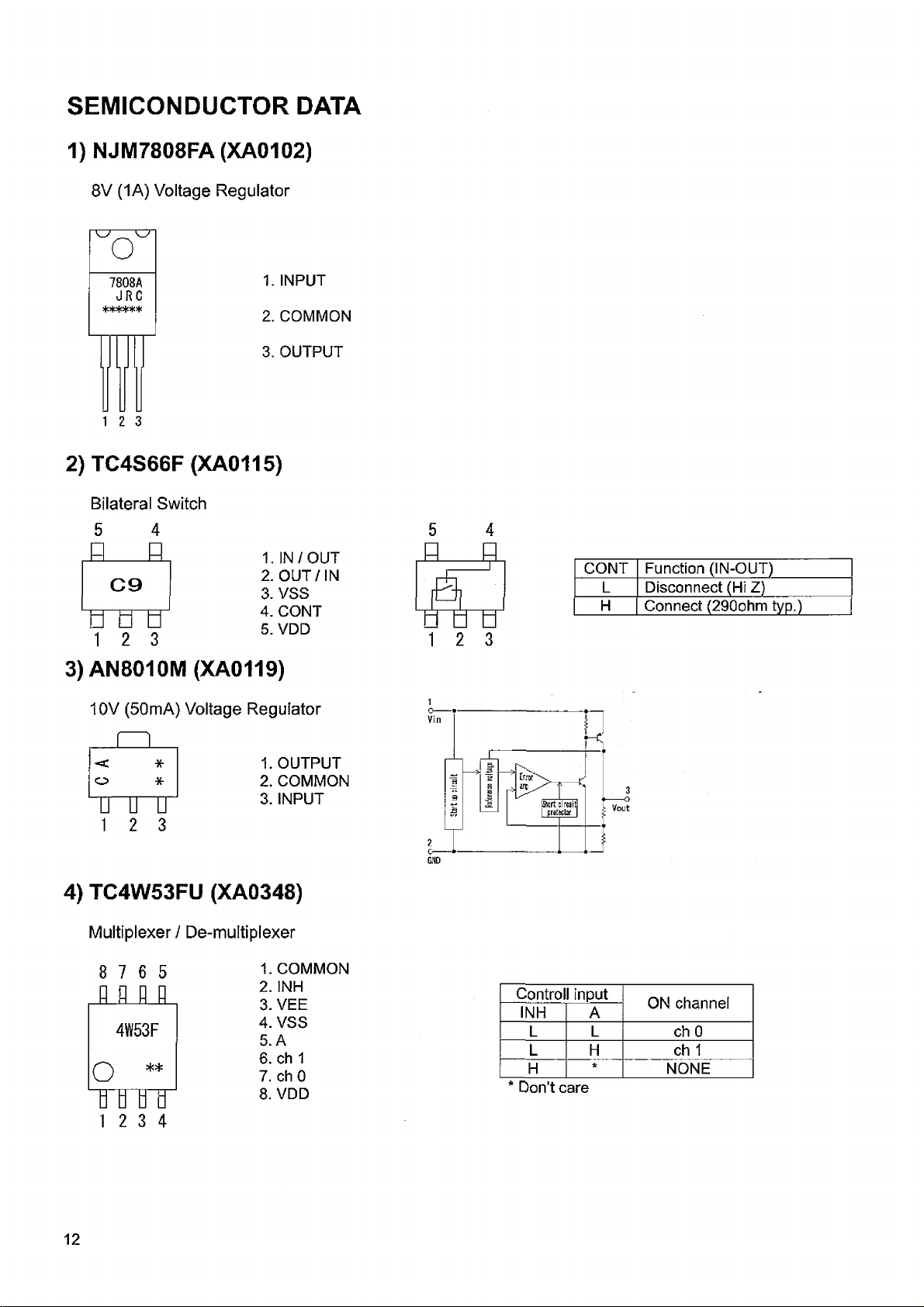
SEMICONDUCTOR DATA
1) NJM7808FA (XA0102)
8V (1A) Voltage Regulator
1. INPUT
2. COMMON
3. OUTPUT
1 2 3
2) TC4S66F (XA0115)
Bilateral Switch
5 4
b
_____
a
C 9
b ti b
1 2 3
1. IN /OUT
2. OUT/IN
3. VSS
4. CONT
5. VDD
3) AN8010M (XA0119)
10V (50mA) Voltage Regulator
i i
•<
o
1. OUTPUT
2. COMMON
3. INPUT
4) TC4W53FU (XA0348)
Multiplexer / De-multiplexer
1. COMMON
2. INH
3. VEE
4. VSS
5. A
6. ch 1
o
T O T
12 3 4
7. chO
8. VDD
5
n
£
e
□ □ ti
1 2 3
CONT Function (IN-OUT)
L Disconnect (Hi Z)
H Connect (290ohm typ.)
Control input
INH A
L L
L H ch 1
H
Don’t care
*
ON channel
chO
NONE
12
Page 13
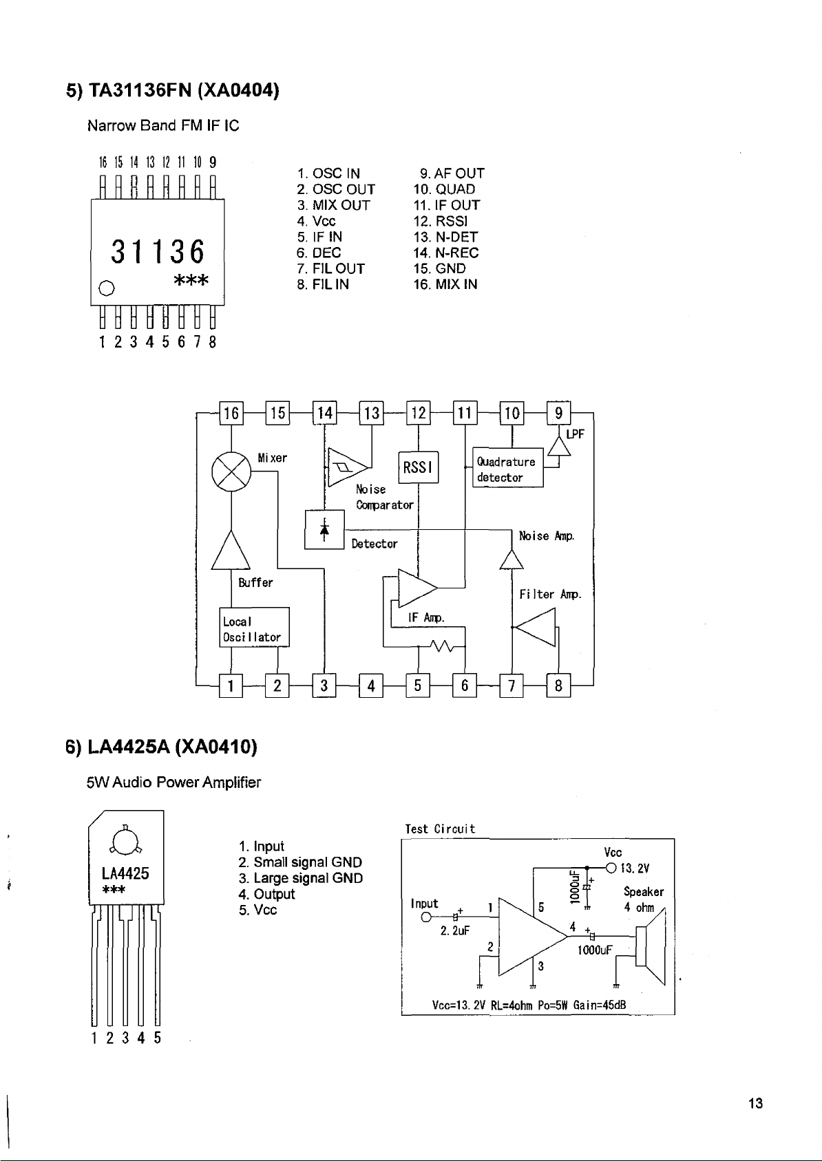
5) TA31136FN (XA0404)
Narrow Band FM IF IC
16 15 14 13 12 11 10 9
1. OSC IN
2. OSC OUT
3. MIX OUT
4. Vcc
5. IF IN
6. DEC
7. FILOUT
8. FILIN
9. AF OUT
10. QUAD
11. IF OUT
12. RSSI
13. N-DET
14. N-REC
15. GND
16. MIX IN
6) LA4425A (XA0410)
5W Audio Power Amplifier
ö .
LA4425
* **
m o m
1 2 3 4 5
1. Input
2. Small signal GND
3. Large signal GND
4. Output
5. Vcc
Test C ircuit
13
Page 14

7) BR24L32FJ (XA0604Z)
32K-Bit EEPROM
8 7 6 5
-ELELfLEL
L3 2
Q * * * * *
m i
2. A1
3.A2
4. Vss
5. SDA
6. SCL
7. WP
8. Vcc
12 3 4
8) S-80845ALMP (XA0620)
4.5V Voltage Detector
5
B 6 6 *
f l
4
1.GND
2. Vin
3. Vout
4. NC
5. NC
1 2 3
9) S-816A50AMC (XA0925)
Name Function
A0...A2 User Configurable Chip Select
Vss Ground
SDA Serial Address / Data / I/O
SCL Serial Clock
WP
Vcc +2.5 - 6.0V Power Supply
Write Protect Input
External Transistor Type 5V Voltage Regulator with On/Off Function
5
B A Z *
b b b
4
R
1. EXT
2. Vss
3. ON/OFF
4. Vin
5. Vout
1 2 3
10) NJM78M05DL1A (XA0947)
5V (500mA) Voltage Regulator
I
-----------
H
1. Input
2. GND
3. Output
14
U
2
-
—
Page 15
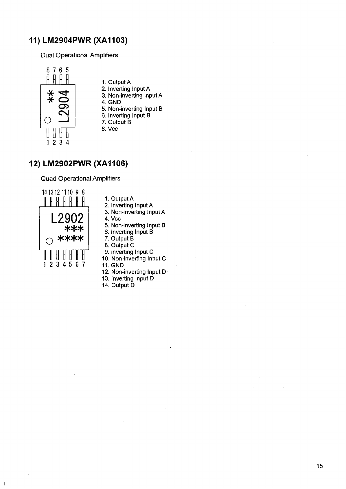
11) LM2904PWR (XA1103)
Dual Operational Amplifiers
8 7 6 5
1. Output A
2. Inverting Input A
3. Non-inverting Input A
4. GND
5. Non-inverting Input B
6. Inverting Input B
7. Output B
8. Vcc
12 3 4
12) LM2902PWR (XA1106)
Quad Operational Amplifiers
10 9 8
1. Output A
2. Inverting Input A
3. Non-inverting Input A
4. Vcc
5. Non-inverting Input B
6. Inverting Input B
7. Output B
8. Output C
1 in I i t
2 3 4 5 6 7
9. Inverting Input C
10. Non-inverting Input C
11. GND
12. Non-inverting Input D
13. Inverting Input D
14. Output D
Page 16
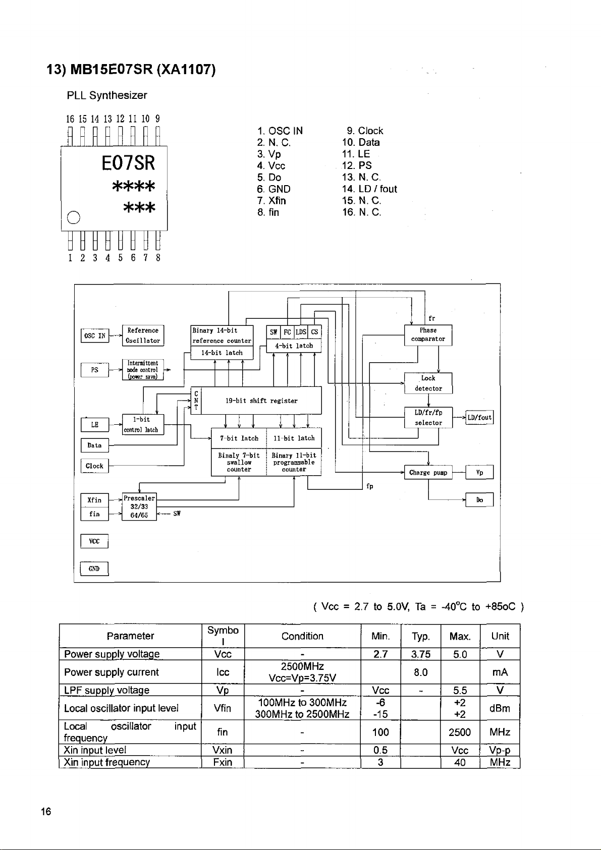
13) MB15E07SR (XA1107)
PLL Synthesizer
16 1 5 1 4 13 1 2 1 1 10 9
HRHRyy
E 0 7 S R
1 2 3 4 5 6 7 8
OSC IN
PS
LE
Data
Clock
Xfin
fin
Reference
Oscillator
Intermittent
mode control
(power saye)
1—bit
control latch
Prescaler
>
32/33
>
64/65
Binary 14-bit
reference counter
14-bit latch
Sff
1.0S CIN 9. Clock
2. N. C. 10. Data
3. Vp 11. LE
4. Vcc 12. PS
5. Do 13. N. C.
6. GND 14. LD/tout
7. Xfin 15. N.C.
8. fin 16. N.C.
Sff FC
19-bit shift register
7-bit latch
Binaly 7-bit
swallow
counter
11-bit latch
Binary 11-bit
programmable
4-bit
counter
LDS CS
latch
fr
Phase
comparator
Lock
detector
LD/fr/fp
selector
Charge pump
fp
LD/fout
Vp
Do
VCC
GND
Parameter
Power supply voltage
Power supply current
LPF supply voltage
Local oscillator input level
Local oscillator input
frequency
Xin input level Vxin
Xin input frequency Fxin
16
Symbo
1
Vcc
Icc
Vp
Vfin
fin
( Vcc = 2.7 to 5.0V, Ta = -40°C to +85oC )
Condition Min.
-
2500MHz
Vcc=Vp=3.75V
-
100MHz to 300MHz
300MHz to 2500MHz
-
-
-
Typ. Max. Unit
2.7 3.75
5.0
8.0
Vcc
-6
-15
-
5.5
+2
+2
100 2500
0.5
3
Vcc
40
V
mA
V
dBm
MHz
Vp-p
MHz
Page 17

14) RA60H1317M1 (XA1108)
144 ~ 146MHz 60W RF Power Module
OUTLINE DRAWING
BLOCK DIAGRAM
(D—lb
© RF In p u t (P in )
(2 ) Gate V o lta g e (VGG), Power C o n tro l
© D rain Vo lta g e (VDD), B a tte r y
@ RF O u tpu t (P o ut)
(5 ) RF Ground (Case)
c?
<0
e*i
ABSOLUTE MAXIMUM RATING ( Tc = 25°C, unless otherwise noted )
Symbol Parameter Conditions
VDD Drain Voltage
VGG
IDD
Gate Voltage
Drain Current
Pin Input Power
Pout
Tease (OP)
Tstg
Output Power
Operation Case Temperature
Storage Temprature
VGG < 5V, ZG = ZL = 50ohm
VDD < 12.5V, Pin=50mW
ZG = ZL = 50ohm
f = 135 -17 5 MHz, Pin=50mW
ZG = ZL = 50ohm
ELECTRICAL CHARACTERISTICS ( Tc = 25 °C, unless otherwise noted)
Symbol Parameter
f
Pout
v I
2fo
Pin
IGG
Frequency Range
Output Power
Total Efficiency
2na Harmonic
Input VSWR
Gate Current
Stability
-
Load VSWR
-
Tolerance
VDD = 12.5V
VGG = 5V
Pin = 50mW
VDD=10.0-15.2V, Pin=25-70mW,
Pout<70W (VGG control), Load
VSWR=3:1
VDD=15.2V, Pin=50mW, Pout=60W
(VGG control),
Load VSWR=8:1
Conditions
Ratings Unit
17 V
5.5 V
15 A
100 mW
80 W
-30 to+110 °C
-40 to +110
Ratings
Min Typ Max
135
175
60
45
-50
3:1
°C
Unit
MHz
W
%
dBc
-
1 mA
No parasitic
oscillation - .
No degradation or
destroy
17
Page 18

15) S-AU82L (XA1142)
400 - 470MHz 60W RF Power Module
OU TLINE DRAWING
BLOCK DIAGRAM
(D RF Input (P in ) ^
(2 ) G a te V o l tage (VGG), P ower C o n tro l
(D D r a in V o ltag e (V DD), B a t tery
(4) RF O utp ut (Pout )
(D RF Ground (Frange)
ABSOLUTE MAXIMUM RATING ( Tc = 25 °C, unless otherwise noted )
Symbol
VDD
Drain Voltage
VGG Gate Voltage
IDD
Pin
Drain Current
Input Power
Pout Output Power
Tease (OP)
Tstg
Operation Case Temperature -30 to +100
Storage Temprature
Parameter
VGG < 5V, Pi = 50 mW, Po < 60W
VDD < 12.5V, Pin=50mW
VDD < 12.5V, VGG < 5V 100
12.5V < VDD < 16.5V, VGG = 5V,
Pi = 50mW
Conditions Ratings Unit
ELECTRICAL CHARACTERISTICS ( Tc = 25 °C, unless otherwise noted )
Symbol Parameter Conditions
f Frequency Range 400 470
Pout Output Power
77 T
2fo
Pin
IGG
Total Efficiency
2na Harmonic '
Input VSWR
Gate Current
VDD = 12.5V
VGG = 5V
Pin = 50mW
ZL = 50ohm
Stability VDD=10.5-16.5V, VGG=0-5V, Pin=50mW,
-
Pout<60W (VGG control), Load VSWR=3:1
ALL PHASE
Load VSWR
-
Tolerance
VDD=10.5-16.5V, VGG=0-5V, Pin=50mW,
Pout=60W (VGG control), Load
VSWR=20:1 ALL PHASE
Min Typ
60 W
40 %
All sprious output
than 60dB bellow
desired signal
No degradation
16.5 V
5.5
15
MW
80 W
°C
-40 to +100 °c
Ratings
Max
Unit
MHz
-30
dBc
3.0
1 mA
V
A
-
-
18
Page 19

16) Transistor, Diode and LED Outline Drawing
Top View
Ml 407
XD0013
DAN235E
XDÓ32Ó"
M
n cr
n
MAZS0270H
" XD0377"
4Z>
C-M—3
DA204U
XD0130
K
n— o'
f t
MA2S111
XD0323
C D
CRG01
XD0391
1SV215
XD0132
4 1 2 }
1SS390
XD0342
UDZS5.6B
XD0395
4c?}
L-M—:
1SV237
XDÓ141
a
_
Q
BB
0 □
a
0
ir
RLs-73
XD0363
DAN222H
XDÖ4Ö0"
_EL
N
U--u
MA728
XD0234
tp Ä }
1SV278
XD0374
VDZ5.1B
XD6462"
1SS355
XD0254
MA4S713
XD0375
n__a
M1N
m o
n n
□ □
S3V60
XD0414
1SV268
XDÓ3ÓÍ
JZZL
m m
. r~i
1SV282
XD0376
4TÖ }
s
2SK880GR
XE0021
G
n
XG
3SK293
XÉÓÓ53
G2 G1
R R
UF
B
g
2SC4245Y
Xt6i 25"
HB
XP1215
XU0178
9M
CQUJ^
2SK2539
XEÖÖ6 6
G
H
AK*
2SC4226
XT0141 "
R24
RN1104
XU0195
XD
n r
FA1111C
XL0069
*
2SB766A
XT0170
b O R
n n r
B C E
EMD6
XÜÖ2Ö9
n n n
i D6 I
FA1 1 1 1C
XL0077
2SC4915
XT0178
Q0
RN1107FV
XÜ6 2 1 6
XH
u— n
2SC4081
XT0095
BR
I ] U
B E
2SB1386
XT0Í90
BHQ
u u u
B C E
RN2107FV
XÜ0211
YH
n— c r
2SA1036K
XT 0110
HQ
2SC5551
XT0194
CO
LU
Ü u u
B C E
2SC4215Y
XT0124
C
n
QY
IT
E
2SD2620J
XÍ02Ó8
C
£L
3B
IT
E
Rb=10kohm
Rbe=none
Rb=47kohm
Rbe=47kohin
Rb=4. 7kohm
Rbe=none
Rb=10kohm
Rbe=47kohm
Rb=10kohm
Rbe=47kohm
19
Page 20

17) LCD Connection (TTR3626UPFDHN)
o a ® 't n r- ^ ^
C i r t r t n CM W n W W (N CM W N r- v ^ i ‘ t - r * ^ - 'r 'r0 5 C D (V N (O W 'f W W r O
( 3 0 0 O O (3 (3 15 O CD O O O O O ( 3 0 0 0 0 0 ( 3 0 0 0 O O O O O O O O O
SEG
COM
n n i- o
5 2 2 2
o o o o
o o o u
LULiiUJ U JLi llULl i LUUJLU UJ LU UJL Utl l L U IU LU U JL U UJ lD U Jl U liJ LULUL UUJ LU ID LU ID LU
wwwwwwototwotwotwwwwwwwwcowwwwotwwwwwotwm
20
Page 21

EXPLODED VIEW
1) Top and Front View
AA 0050
DR-135
DR-435
NK 0073
!
21
Page 22

2) Bottom View
AU0001
ST0065
ES0035
ST0066
TG0034
Page 23

3) LCD Assembly
FF0017
23
I
Page 24

PARTS LIST
CPU Unit
Ref No. Part No. DBScription
CU35S4
C1
C2
CU3554 Chip C. GRM155B11A104KA01D
C3 CU3549
C4 CU3549
C5
CU3554 Chip C.
C6 CU3523
C7 CU3523
CU3543
C8
CU3554 ChipC.
C9
C10 CU3543
CU3543
C11
C12
CU3553
CS0049 Chip tantalum TMCSA1C105MTRF 1 1
C13
C14 CU3514
C15
CU3514 Chip C.
C16
CU3535
CS0424
C17
C18 CU353S
CU3554 Chip C.
C19
C20 CU3547
C21 CU3547
C22 CU3535
C23
CU3547 Chip C. GRM155B11C103KA01D
C24 CU3535
C25
CU3535
C26
CU3535 ChipC.
C27
CU3535 Chip C.
CN1 UE0291 Connector 17R-JE(LF)(SN) 1 1
CN2 UE0291 Connector
CN3
UE0035 Mic Connector
D1
XL0069 Chip LED FA1111C-TR 1 1
XL0077
D2
D3
XLD077 Chip LED FA1111C-732-TR
D4 XL0D69 Chip LED
XL0077
D5
D6 XL0077
D8
XD0323
D9 XD0234
XL0077
D11
D17 XD0234
IC1 XA1130 CPU CPU DR136MK3
IC2 XA0604Z
XA0620
IC4
IC6
XA0348
JK1 UJ0047 Jack HSJ2013-01-120 1 1
MACL04G Wire #30AH1-040-H1 1 1 FXE
JP3
LCD1 EL0049
Q4
XU0210
QS
XT0095 Chip 2SC4081 T106R
XT0170
Q7
QB
XU0210 Chip RN1107MFVfTPL3)
Q10
XU0210 Chip RN1107MFV(TPL3) 1 1
XU0211 Chip RN2107FV (TPL3) 1 1
Q11
XU0211
Q12
R1 RK3554 Chip R.
R4 RK3554 Chip R. ERJ2GEJ223X 1 1
R5 RK3550
R6 RK3550
R7 RK3026 Chip R. MCR03EZPJ101
RK3026
R8
R10
RK3032 Chip R.
R11 RK3546 Chip R. ERJ2GEJ472X
R13 RK3001 Chip R. MCR03EZPJOOO 1 1 FXE
R14 RK3S48
R15 RK35D1
R16
RK3001 Chip R, MCRD3EZPJOOO 1 1 FX
R19 RK3562 Chip R.
R20
RK3546 Chip R. ERJ2GEJ472X
R22
RK3538 Chip R. ERJ2GEJ102X 1 1
R25 RK3550
R2G
RK3S50 Chip R. ERJ2GEJ103X
R27
RK3550 Chip R.
R28 RK3538
R29 RK3538 Chip R. ERJ2GEJ102X
R30
RK3538 Chip R. ERJ2GEJ102X 1 1
R32
RK3544 Chip R. ERJ2GEJ332X
R33
RK3534 Chip R. ERJ2GEJ471X
R34 RK3547
R35
RK3552 Chip R. ERJ2GEJ153X
R36
RK3562 Chip R. ERJ2GEJ104X 1 1
R37 RK3549 Chip R. ERJ2GEJ822X 1 1
R38
RK3551
R39 RK3558 Chip R. ERJ2GEJ473X 1 1
R40 RK3562 Chip R. ERJ2GEJ104X 1 1
R41
RK3526 Chip R. ÉRJ2GEJ101X
R42
RK3550 Chip R. ERJ2GEJ103X 1 1
Chip C.
Chip C.
Chîp C.
Chip C.
Chip C.
Chip C.
ChipC.
Chip C.
Chip C.
Chip C.
Chip C.
Chip tantalum TMCMA1C106MTR 1
ChipC. GRM15SBUH1Q2KAQ1D
Chip C.
Chip C.
Chip C. GRM155B11H102KA01D
Chip C.
Chip C.
Chip LED
Chip LED FA1111C-732-TR 1 1
Chip LED FA1111C-732-TR
Chip Diode
Chip Diode
Chip LED
Chip Diode
iC
IC SB0845CLMC-B66-T2G
TC4W53FU
LCD
Chip RN11D7MFV(TPL3)
Chip
Chip
Chip R. ERJ2GEJ103X
Chip R. ERJ2GEJ103X
Chip R, MCR03EZPJ101 1 1
Chip R. ERJ2GEJ682X
Chip R. ERJ2GEOROOX 1
Chip R. ERJ2GEJ103X
Chip R. ERJ2GEJ102X
Chip R.
ChipR.
Parts Name
5Sm 155B11A104KA01D
GRM155B11C153KA01D
GRM155B11C153KA01D
GRM155B11A104KA01D 1
GRM1552C1H101JD01D
GRM1552C1H101JD01D 1 1
GRM155B11E472KA01D 1 1
GRM155B11A104KA01D
GRM155B11E472KA01D 1 1
GRM155B11E472KA01D 1 1
GRM155B11A473KA01D
GRM1552C1H180JZ01D
GRM1552C1H180JZ01D
GRM155B11H102KA01D 1 1
GRM155B11A104KA01D 1
GRM155B11C103KA01D 1 1
GRM155B11C103KA01D
GRM155B11H102KA01D
GRM155B11H102KA01D 1 1
GRM155B11H102KA01D 1
GRM155B11H102KA01D
17R-JE{LF)[SN)
MIC FM214-8SMPY
FA1111C-732-TR
FA1111C-TR
MA2S1110QL
MA2J72800L 1 1
FA1111C-732-TR 1 1
MA2J72800L 1 1
BR24L32FJ-WE2 1 1
T C4WS3FU(TE 12 L)
TTR3626 UPTDHN
2SB0766ARL 1
RN2107FV (TPL3)
ERJ2GEJ223X
MCR03E2PJ331 1 1
ERJ2GEJ104X 1 1
ERJ2GEJ103X
ERJ2GEJ562X 1 1
ERJ2GEJ123X
DR-135
1
1
1
1 1
1 1
1 1
1
1 1
1 1
1
1 1
1 1
1
1 1
1 1
1 1
1
1 1
1
1 1
1 1
1 1
1
1 1
1
1 1
1
A
1
1 1
1
1 1
1
1
1
1 1
1
1 1
1
1 1
1
1
1
1
1
1
Qty.
DR-435
Ver.
1
1
1
1
1
1
1
1
1
1
1
1
1
A
1
1
1
1
1
1
1
1
1
1
1
1
1
1
Ref No. Part No. Description Parts Name
R43
RK3550 Chip R. ERJ2GEJ103X
R44
RK3026 Chip R.
R45
RK3550 Chip R. ERJ2GEJ103X
R48 RK3538
R50 RK3570
R51
RK3538 Chip R. ERJ2GEJ102X
RK3538
R52
R53 RK3562
R54
RK3550
RS5
RK3574
R56 RK3550 Chip R. ERJ2GEJ103X 1 1
R57
RK3566 Chip R. ERJ2GEJ224X
R58
RK3534 Chip R. ERJ2GEJ471X 1 1
R59 RK3526 Chip R.
R60 RK3034
R61
RK3574 Chip R. ERJ2GEJ105X
R62 RK3550 Chip R. ERJ2GEJ103X 1 1
R63 RK3526
RK3549
R64
R65
RK3526 Chip R. ERJ2GEJ101X
R66 RK3550 Chip R.
R67 RK3526
R68
RK3550 Chip R. ERJ2GEJ103X
R70
RK3562 Chip R. ERJ2GEJ104X 1 1
R71 RK3574
R72 RK3550
R73
RK3032 Chip R. MCR03EZPJ331
R74 RK3526 Chip R.
R76 RK3532
R79
RK3538 Chip R. ERJ2GEJ102X
R80
RK3538 Chip R. ERJ2GEJ102X 1 1
R83 RK3538 Chip R. ERJ2GEJ102X 1 1
R85 RK3546
R87
RK3S54
R88 RK3550 Chip R. ERJ2GEJ103X 1 1
R89 RK3558
R90 RK3558
R98
RK3501 Chip R. ERJ2GEOROOX 1 1
RE1 UR0015 Dial
SW1 UU0015Z Switch EVQPPPA25 1
SW1
UU0042
SW2 UU0016Z
SW2 UU0042 Switch SKQYAAE010 1
SW3
UU0015Z
SW3
UUQQ42
UU0015Z
SW4
UU0042
SW4
SW5
UU0015Z
SW5 UU0042 Switch SKQYAAE010 1
UU0015Z
SWS
sws
UU0042
SW7
UU0015Z
SW7 UU0042
VR1 RV0035 Variable R.
X1
XQ0131
DGQ037
FG0305
FM0034
FP0034
FP0234
ST0064
ST0068
TL0023
TL0024
YZ0042
Chip R.
Chip R.
Chip R. ERJ2GEJ102X 1 1
Chip R.
Chip R. ERJ2GEJ103X
Chip R. ERJ2GEJ105X
Chip R. MCR03EZPJ471
ChipR.
Chip R. ERJ2GEJ822X
Chip R.
Chip R.
Chip R. ERJ2GEJ103X
Chip R.
Chip R. ERJ2GEJ472X
Chip R. ERJ2GEJ223X
Chip R.
Chip R. ERJ2GEJ473X
Switch
Switch
Switch
Switch
Switch EVQPPPA25 1
Switch
Switch
Switch
Switch
Switch
Switch
Xta!
MCR03EZPJ101 1 1
ERJ2GEJ102X 1 1
ERJ2GEJ474X
ERJ2GEJ104X
ERJ2GEJ101X
ERJ2GEJ101X 1 1
ERJ2GEJ103X
ERJ2GEJ101X 1 1
ERJ2GEJ105X 1 1
ERJ2GEJ101X
ERJ2GEJ331X 1 1
ERJ2GEJ473X
R H90 N74E20-A90770
SKQYAAE010 1
EVQPPPA25 1
EVQPPPA25
SKQYAAE010 1
SKQYAAE010
EVQPPPA25
EVQPPPA25
SKQYAAE010 1
EVQPPPA25 1
SKQYAAE010 1
EVUF2JFK4B14
CSA310 3.6864MHZ
LCD LIGHT DR135
LCD RUB.CONNECT.
MIC GND PLATE
MIC SPACER DR110
MICSPACERA DR135
LCD HOLDER DR135
DIAL FITTING DR135
REFLECTION DR135
DIFFUSION SHEET 135
CEMENT G17/1G
Qty.
DR-135 DR-435
1
1 1
1 1
1 1
1 1
1 1
1
1 1
1 1
1 1
1 1
1 1
1
1 1
1 1
1 1
1
1 1
1
1 1
1
1 1
1 1
1 1
1
1
1
1 1
1
1
1
1
1
1
1
1
1
1
1
MA N Uni DR-135
Ref No.
Part No. Description Parts Name Qty. Ver.
C104 CU3047 Chip t. C1608JB1H103KT-NS
C105 CS0394
C107
CU3554 Chip C.
C108 CU3547 Chip C. GRM155B11C103KA01D
C109 CE0339 Electrolytic C. 16ME10SWB+TS-ALC
c m CU3554 Chip C.
C112 CU3554
C113
CU3047
CU3547 Chip C.
C114
C116 CU3019 Chip C.
C117
CU3547
C120 CU3522 Chip C.
CU3503
C121
C122
CU3502
C123 CU3515 Chip C.
Chip tantalum
Chip C.
Chip C.
Chip C. GRM155B11C103KA01D
Chip C.
Chip C.
TMCMB0J476MTRF
GRM 155B11A1Q4KA01D
GRM155B11A104KA01D
GRM155B11A104KA01D
C1608JB1H103KT'NS
GRM155B11C103KA01D
C1608CH1H470JT-NS
GRM1552C1H820JD01D
GRM1554C1H2R0CZ01D
GRM1554C1H1R0CZ01D
GRM 1552C1H220JZ01D
\
1
1
1
1
1
1
1
1
1
1
1
1
1
Ver.
1
1
1
1
1
1
1
1
1
1
1
1
1
1
1
1
1
1
24
Page 25

Ref No. PartNo. Description
cuchos
C13D
C131
CU3535 Chip C.
CU3535
C132
CU3503
C133
C135 CU3547 Chip C.
C136 CU3011
C137 CU3517 ChipC. GRM1552C1H330JZ01D
C139 CU3517 Chip C.
C140
CU3517 Chip C.
CU3554
C143
C144 CU3547 Chip C. GRM155B11C103KA01D
C145 CU3503
C146 CE0364 Electrolytic C.
C148 CU3517 Chip C. GRM1552C1M330JZ01D
C149 CU3517 Chip C.
C151 CU3547 Chip C. GRM155B11C103KA01D
C152
CE0339 Electrolytic C.
C153 CU353S Chip C.
CU3535
C154
CU3506
C155
CU3535
C157
C150 CU3535 Chip C.
CU3535
C159
C163 CU3535 Chip C. GRM155B11H102KA01D
C164 CU3535 Chip C. GRM155B11H102KA01D
C165 CU3559
C166 CE0420 Electrolytic C.
C169 CU3527 Chip C. GRM1552C1E221JD01D
C170 CU3554 Chip C.
C171 CU3515 Chip C.
C173 CU3535 Chip C. GRM155B11H102KA01D
C174 CU3527 Chip C.
C175 CU3535
C178 CU3554 Chip C. GRM155B11A104KA01D
C179 CU3554 Chip C. GRM155B11A104KA01D
C180 CU3535
C183 CU3035 Chip C.
C185 CS0232
CU3511
C186
0187 CU3535
C188 CU3535 Chip C. GRM155B11H102KA01D
CU3019
C189
C190 CU3547 Chip C. GRM155B11C103KA01D
C191 CU3552 Chip C.
C193 CU4033 Chip C. GRM31BR72J102KW01L
CU3019
C194
CU3015
C195
CU3516
C196
C199 CE0339 Electrolytic C.
C200
CU3035 Chip C.
C201 CU4013 Chip C. GRM42-6CH150J500PT
C2D2 CU4016
C203 CU4016
C204 CU4011 Chip C. GRM42-BCH100D500PT
C205
CU3035 Chip C.
C206
CE0339
C207 CU3064 Chip C. C1608CH1H1R5CT-NS
C208 CU3064 Chip C. C1608CH1H1R5CT-NS
C209 CU3035
C210 CU3011 Chip C. C1608CH1H100DT-NS
CU3011
C211
CE0364
C212
CU3035
C213
C215 CU4015 Chip C. GRM42-6CH220J500PT
CU4015
C216
CU3551
C217
CU3551
C218
C219 CU3035 Chip C.
C220
CU3035
C222 CU3535 Chip C. GRM155B11H102KA01D
CE0384
C223
CU3023
C224
C225 CU3035 Chip C. C1608JB1H102KT-NS
CU3035
C226
CU0108
C227
C228 CU3S35 Chip C. GRM155B11H102KA01D
C229 CU3553 Chip C. GRM155B11A473KA01D
CU3535
C230
C231 CU3535 Chip C. GRM155B11H102KA01D
C232 CU3535
C233 CU3535 Chip C. GRM155B11H102KA01D
C235 CU3504 Chip C. GRM1553C1H3R0CZ01D
C237 CU3535 Chip C. GRM155B11H102KA01D
C238 CU3111 Chip C. C1608JB1E104KT-NS
C239 CU3535 Chip C. GRM155B11H102KA01D
C241 CU3522
C242 CU3551 Chip C. GRM155B11C223KA01D
C243 CEO339
C244 CE0339 Electrolytic C. 16ME10SWB+TS-ALC
CU010B
C245
|C24B
CU3543 Chip C. GRM155B11E472KA01D
ChipC. LMK212BJ105KG-T
Chip C. GRM155B11H102KA01D
Chip C. GRM1554C1H2R0CZ01D
Chip C.
Chip C. GRM155B11A104KA01D
Chip C. GRM1554C1H2ROCZ01D
Chip C. GRM155B11H102KA01D
Chip C. GRM1552C1H5RQCZ01D
Chip C. GRM155B11H102KA01D
Chip C. GRM155B11H102KA01D
Chip C. GRM155B30J105KE18D
Chip C.
Chip C.
Chip tantalum
Chip C. GRM1552C1H100JZ01D
Chip C.
Chip C.
Chip C.
Chip C. C16D8CH1H220JT-NS
Chip C. GRM1552C1H270JZ010
Chip C. GRM42-6CH270J50DPT
Chip C. GRM42-6CH270J500PT
Electrolytic C.
Chip C.
ChipC. C1608CH1H10ODT-NS
Electrolytic C.
Chip C. C1608JB1H102KT-NS
Chip C. G R M42-6CH22 0 J500PT
Chip C. GRM155B11C223KA010
Chip C.
Chip C. C1608JB1H102KT-NS
Electrolytic C.
Chip C.
Chip C.
Chip C. LMK212BJ105KG-T
Chip C. GRM155B11H102KA01D
Chip C.
Chip C.
Electrolytic C.
Chip C. UMK212BJ105KG-T
Parts Name
GRM155B11H102KA01D
GRM155B11C103KA01D
C1608CH1H10ODT-NS
GRM1552C1H330JZ01D
GRM1552C1H330JZ01D
18ME47SWB+TS
GRM1552C1H330JZ01D
16ME1QSWB+TS-ALC
GRM155B11H102KA01D
GRM155B11H102KA01D
1SME22SZ
GRM155B11A104KA01D
GRM1552C1H220JZ01D
GRM1552C1E221JD01D
GRM155B11H102KA01D
GRM155B11H1Q2KA01D 1
C1608JB1H102KT-NS 1
TMC MA1V474MTRF
GRM155B11H102KA01D
Ci 608CH1H470JT-NS
GRM155B11A333KA01D
C1608CH1H470JT-NS
16ME10SWB+TS-ALC
C16D8JB1H102KT-NS
C1608JB1H102KT-NS
16ME10SWB+TS-ALC
C1608JB1H102KT-NS
16ME47SWB+TS
GRM155B11C223KA01D
C1608J B1H102KT-NS
16ME47SWB+TS
C1608CH1H101JT-NS
C1608JB1H102KT-NS
GRM155B11H102KA01D
GRM1552C1H820JD01D
16ME1OSWB+TS-ALC
Qty.
Ref No. Part No.
Ver.
1
1
1
1
1
1
1
1
1
1
1
1
1
1
1
1
1
1
1
1
1
1
1
1
1
1
1
1
1
1
1
1
1
1
1
1
1
1
1
1
1
1
1
1
1
1
1
1
1
1
1
1
1
1
1
1
1
1
1
1
1
1
1
1
1
1
1
1
1
1
1
1
1
1
1
1
1
1
1
1
1
1
1
ÔU3547
C248
C249 CU3538 Chip C.
CU3526
C250
C252 CU3535
C253 CU3549 Chip C.
C254 CU3111 Chip C. C1608JB1E104KT-NS
CE0364
C255
C256 CU3111 Chip C.
C257 CE0339 Electrolytic C. 16ME10SWB+TS-ALC
C258 CU0108 Chip C.
C260 CE0339
C261 CU3535 ChipC.
CU3535 Chip C.
C262
CS0424 Chip tantalum
C263
C264 CU3519 ChipC.
CU3535 ChipC.
C265
C266 CU3503 ChipC.
C267 CU3535 ChipC.
C268 CU3535 Chip C.
CU3535 ChipC. GRM155811H102KA01D
C269
C270 CU3047 ChipC.
C271 CU3535 Chip C.
C272 CS0220 Chip tantalum
CS0220
C273
C274 CU3535 Chip C.
C275 CU3547 Chip C.
C276 CE0339 Electrolytic C. 16ME10SW B+TS-A LC
CE0343 Electrolytic C. 16ME1000HC+T
C277
C278 CU3535 Chip C.
C279 CU3551 ChipC.
CU3512 ChipC.
C281
C282 CU3502 ChipC.
C283 CU3531 ChipC.
C284 CU3502 ChipC.
C285 CU3535 ChipC.
C266
CU3027 ChipC.
C287 CS0063 Chip tantalum
C288
CU3511 ChipC.
C289 CU3535 ChipC:
C290 CU3535 ChipC.
CU3535
C293
C294 CU3035 ChipC.
C295 CU3551 Chip C.
C296 CU3511 Chip C.
CU3535
C297
C299 CU3547 Chip C.
C300
CU3515 Chip C.
C301 CU3523 Chip C.
C302 CU3523
C303 CU3523 Chip C.
CU3535 Chip C.
C304
C305 CU3547 Chip C.
C306 CU3554 Chip C.
C307 CU3547 Chip C.
C308 CE0342
C309 CU3551 Chip C.
C310 CU3523 Chip C.
CU3511 ChipC.
C312
C313 CU3535 ChipC.
C321 CS0220 Chip tantalum
C322 CU3035 ChipC.
CU0108
C326
C331 CU3547 ChipC.
C332 CE0339 Electrolytic C.
C333 CU3535 Chip C.
C401 CU3549 Chip C.
C402 CU3550 Chip C.
C403 CU3552 Chip C.
C404 CU3559
C405 CU3542 Chip C.
C40B CU3545 Chip C.
C407 CU3541 ChipC.
C408 CU3544 ChipC.
C409 CU3535 ChipC.
C410 CU3539 ChipC,
CU010S
C412
C413 CU3541 Chip C.
C414 CU3542 Chip C.
C415 CU3545 Chip C.
C417 CU3547
C418 CU3547 Chip C.
CU3547 Chip C.
C419
C427 CU3559 Chip C.
C428 CU0110 ChipC.
CU3515
C601
C607 CU3511
C611 CU0108 Chip C.
CU3515 Chip C.
C613
CN101 UE0369
CN102 UE0293 Connector
UE0293
CN103
Description
Chip C.
Chip C.
Chip C.
Electrolytic C. 16ME47SWB+TS
Electrolytic C. 16ME10SW B+TS -A LC
Chip tantalum
ChipC.
ChipC.
Chip C.
Electrolytic C.
ChipC. LMK212BJ105KG-T
Chip C.
Chip C.
Chip C.
ChipC.
Chip C.
Connector AXN49301616
Connector 17PS-JE
Parts Name
GRM 155B11C103KA01D
GRM155B11H182KA01D
GRM1552C1E181JD01D
GRM155B11H102KA01D
GRM155B11C153KA01D
C1608JB1E104KT-NS
LMK212BJ105KG-T
GRM155B11H102KA01D 1
GRM155B11H102KA01D 1
TMCMA1C106MTRF
GRM1552C1H470JZ01D
GRM155B11H102KA01D 1
GRM1554C1H2R0CZO1D
GRM155B11H102KA01D
GRM155B11H102KA01D 1
C1608JB1H103KT-NS
GRM 155811H102KA01D
TMCMA1C225MTRF 1
TMCMA1C225MTRF
GRM155811H102KA01D
GRM155B11C103KA01D 1
GRM155B11H102KA01D
GRM155B11C223KA01D 1
GRM1552C1H120JZ01D 1
GRM1554C1H1R0CZO1D
GRM155B11H471KA010
GRM1554C1H1R0CZO1D 1
GRM155B11H102KA01D 1
C1608CH1H221JT-NS 1
TMCSA1V104MTRF 1
GRM1552C1H100JZ01D 1
GRM155B11H102KA01D
GRM155B11H102KA01D 1
GRM155B11H102KA01D 1
C1S08JB1H102KT-NS
GRM155B11C223KA01D
GRM1552C1H100JZ010 1
GRM155B11H102KA01D 1
GRM155B11C103KA01D
GRM1552C1H220JZ01D
GRM1552C1H101JD01D 1
GRM1552C1H101JD01D
GRM1552C1H101JD01D
GRM155B11H102KA01D 1
GRM155B11C103KA01D 1
GRM155B11A104KA01D
GRM155B11C103KA01D 1
16ME470HC+TS
GRM155811C223KA010
GRM1552C1H101J001D
GRM1552C1H100JZ010
GRM155B11H102KA01D 1
TMCMA1C225MTRF
C1608JB1H102KT-NS
GRM155B11C103KA01D
10ME1OSWB+TS-ALC
GRM155B11H102KA010 1
GRM155811C153KA01D
GRM 155811C183KA01D
GRM155B11A333KA01D
GRM155B30J105KE18D 1
GRM155B11H392KA01D
GRM155B11E882KA01D
GRM155B11H332KA01D
GRM155B11E562KA01D
GRM155B11H102KA01D
GRM155B11H222KA01D 1
LMK212BJ105KG-T
GRM155B11H332KA01D
GRM155B11H392KA01D
GRM155811E682KA01D
GRM155811C103KA01D
GRM155B11C103KA01D
GRM155B11C103KA01D
GRM155B30J105KE18D 1
C2012JB1A475KT-NS
GRM1552C1H220JZ01D
GRM1552C1H1OOJZOID
LMK212BJ105KG-T
GRM1552C1H220JZ01D
17PS-JE
Qty. Ver.
1
1
1
1
1
1
1
1
1
1
1
1
1
1
1
1
1
1
1
1
1
1
1
1
1
1
1
1
1
1
1
1
1
'
1
1
1
1
1
1
1
1
1
1
1
1
1
1
1
1
1
1
1
1
1
1
1
1
1
1
1
1
1
1
25
i
Page 26

Ref No.
Part No.
CN104 UA0037AY
CN106 UE0043
D102 XD0132
D103
XD0132
D104
XD0132
D105 XD0132
D106
XD0402
D108 XD0130
D1Q9 X00301
D110 XD0013
D111 XD0375
D112 XD0375
D113 XD0323
D114 XD0141
D115 XD0320 Chip Diode DAN235E-TL
D116 XD0320
D11B XD0130
D119 XD0323 Chip Diode MA2S11100L
D120
XD0374
D121 XD0414
0122 XD0376
0123 XD0376
D125 XD0342
D130 XD0323
D136 X00395 Chip Diode UDZS TE-17 5.6B
D402 X0D323
XD0131 Chip Diode
D601
FL101 XC0070
FL102
XC0052
IC101 XA0947 IC
IC104 XA1106 1C
IC 108 XA0404
IC109 XA0115
IC110 XA1108 IC
IC111 XA0115 IC TC4S66F(TE85R,F)
XA0115
IC113
IC114 XA11D6 IC
IC115 XA0102 IC
IC11S XA1107 IC
IC117 XA0410
IC120 XA1103 IC
IC601 XA1135 IC
JK102 UJ0024Z
L101
QC0043
L102 QA0112 Coil
L103 QA0112 Coil
L104 QA0112
L105 QA0112 Coil
L111 QKA45E Coil
QKA35D
L112
L113
QKA45E Coil
L114 QKA45E Coil
L115 QKA45E Coil MR3.04.5T 0.8
L116
QKA45E Coil
QC0065 Chip Inductor
L117
L118 QKA95D Coil
L119 QC0542 Chip Inductor LQW2BHN R22 J03L
L120
QC0534
QC0292 Chip Inductor
L121
L122 QC0288 Chip Inductor N LV25T-1R0J-PFS
QA0162
L123
L124 QC0732
L125 QC0627
L126 QC0288
L129 QC0534
Q104 XU0210 Chip
Q105 XT0178 Chip 2SC4915-0{TE85L, F)
Q106
XE0053 Chip FET 3SK293{TE85L,F)
Q107 XE0053
Q108 XU0210 Chip RN1107MFV{TPL3)
Q109 XT0208
Q110 XT0208 Chip
Q115 XT0194 Chip 2SC5551-TD-E
Q116 XT011D
Q117 XT0095 Chip
Q120 XU0210 Chip RN1107MFV(TPL3)
Q121
XU0178 Chip
Q122
XT0190 Chip 2SB1366 T100Q
Q123 XT0170 Chip 2SB0766ARL
Q124
XU02Q9 Chip
Q125 XE0021
XU0210
Q126
XT0095
Q127
Q128 XU0210 Chip RN1107MFV(TPL3)
Q129 XU019S
Q131 XE0066
XU0210
Q132
Q133 XU0210
Q134 XT0178 Chip
Q135 XT0178 Chip 2SC4915-0(TE85L,F)
Q137 XU0210 Chip
Description
Wire
Connector P122A02M
Chip Diode
Chip Diode 1SV215(TPH2,F)
Chip Diode
Chip Diode
Chip Diode
Chip Diode
Chip Diode
Diode L407CDB
Chip Diode
Chip Diode
Chip Diode
Chip Diode
Chip Diode
Chip Diode
Chip Diode
Diode S3V60-5000
Chip Diode
Chip Diode
Chip Diode
Chip Diode
Chip Diode
Ceramic Filter
Ceramic Filter ALFYM450G=K
IC
IC
IC
IC
Jack LGY6501-0900FC
Chip Inductor
Coil
Coil MR3.0 3.5T 0.6
Chip Inductor
Coil
Chip Inductor
Chip Inductor
Chip Inductor
Chip inductor
Chip FET
Chip
Chip
Chip FET
Chip
Chip
Chip
Chip FET
Chip RN1107MFV(TPL3)
Chip
Parts Name Qty.
R-B2.0X0.2M PLUG 15A
1SV215(TPH2,F)
1SV215(TPH2,F)
1SV215(TPH2,F)
VD2T2R 5.1 B
DA204U T106
1SV268-TD-E
MA4271300L
MA4Z7130QL
MA2S11100L
1 SV237(TE85L, F)
DAN235E-TL
DA204U T106
1SV278(TPH2,F)
1SV282(TPH2,F)
1 SV282(TPH2,F)
1SS390 TE61
MA2S11100L
MÄ2S-S1100L
1SV214(TPH4,F)
ALFYM450E=K
N JM78M05DL1 ATE1#ZZ
LM2902PWR
TA31136FNG(EL)
TC4S66F(TE85R,F)
RA60H1317M1 -101
TC4S66F(TE85R,F)
LM2902PWR
NJM7808FA-#ZZZB
MB15E07SRPFTGBNDE
LA4425A-E
LM2904PWR
74LV1GW04ASCE-E
NLV32T-2R2J-PFS
#V666SNS-063DAQ
#V656SNS-063DAQ
#V666SNS-063DAQ
#V666S NS-063DAQ
MR3.0 4.5T 0.8
MR3.04.5T 0.8
MR3.0 4.5T 0.8
MR3.04.5T 0.8
NLV32T-068J-PFS
MR3.0 9.5T 0.6
LQW2BHN47NJ03L
N LV25T-2R2 J-P FS
#657B N -1652G NA= P3
LK10051ROK-T
LL1608-FSLR10J
NLV25T-1ROJ-PFS
LQW2BHN47NJ03L
RN1107MFV(TPL3)
3SK293(TE85L,F)
2SD2620JOL
2SD2620JOL
2SA1038K T146Q
2SC4081 T106R
XP0121500L
EMD6T2R
2SK880-GR(TE85L,F)
RN 1107MFV(TPL3)
2SC4081 T10SR
RN1104(TE85L,F)
2SK2539-TB-E
RN1107MFVfTPL3)
2S C4915-0(TE85L, F)
RN1107MFV(TPL3)
«. 1
Ver.
1
1
1
1
1
1
1
1
1
1
1
1
1
1
1
1
1
1
1
1
1
1
1
1
\
1
1
1
1
1
1
1
1
1
1
1
1
1
1
1
1
1
1
1
1
1
1
1
1
1
1
1
1
1
1
1
1
1
1
1
1
1
1
1
1
1
1
1
1
1
1
1
1
1
1
1
1
1
1
1
1
1
1
1
1
1
1
Part No.
Ref No.
Q138 XU0210
Q141 XU0211
Q144
XT0095
Q145 XT0124
Q147 XU0209
Q148 XU0195
Q149 XU0210
Q401 XU0210
Q402 XU0211
R105 RK3530
R106 RK3554
RK3554
R107
R109 RK3526
R110 RK3526
R112 RK3526
R113 RK3542
R114 RK3540
R116 RK3534
R117 RK3562
R118 RK3526
R125 RK3541
R126
RK3552
R128 RK3562
R129 RK3550
R130 RK3562
R131
RK35S2
R132 RK3550
R133 RK3538
R134 RK3553 Chip R.
R136 RK3534
R143 RK3542
R144 RK3542 Chip R.
R145 RK3552
R146 RK3552
RK3550
R147
R148 RK3538
R149 RK3562
R151 RK3550
R152 RK3538 Chip R.
R153
RK3562
R155 RK3552
R156 RK3558
R157 RK3562 Chip R.
R158 RK3522
R160 RK3562
R161 RK3562 Chip R.
R162 RK3521
R163 RK3514
R164 RK3025
R165 RK3574
R166 RK3562
R167 RK3564
R168 RK3554 Chip R.
R171 RK3562
R172 RK3562
R173 RK3526 Chip R.
RK3544
R178
R183 RK3568
R184 RK3526
R185
RK3570
R186 RK3562
R187 RK3558
R189 RK353S Chip R.
R190 RK3538
RK3538
R191
R193 RK3538
R195 RK3570
R196 RK3538
R200 RK3S70
R202 RK0028
R203 RK3556
R204 RK3562
R205
RK0069
R206 RK0003
R207 RK3552
R208
RK3534 •
R209 RK3561 •
R210 RK3538 Chip R.
R211 RK4018
R212 RK4026
R213
RK3549
R214 RK3550
R215 RK3543 Chip R.
R216
RK3050
R217 RK3050
RK3554 Chip R.
R218
R219 RK3538
R220 RK4034
R222 RK3550 Chip R.
R223 RK3526
R224 RK3526
Description Parts Name
Chip
Chip RN2107MFV(TPL3)
Chip
Chip
Chip EMD6T2R
Chip
Chip
Chip
Chip RN2107MFV(TPL3)
Chip R.
Chip R.
Chip R. ERJ2GEJ223X
Chip R.
Chip R.
Chip R. ERJ2GEJ1Û1X
Chip R.
Chip R.
Chip R.
Chip R.
Chip R.
Chip R.
Chip R.
Chip R.
Chip R.
ChipR.
Chip R.
Chip R.
Chip R.
Chip R.
Chip R.
Chip R.
Chip R.
Chip R.
Chip R.
Chip R.
Chip R.
Chip R.
Chip R.
Chip R.
Chip R.
Chip R.
Chip R.
Chip R.
Chip R. MCR03EZPJ820
Chip R.
Chip R.
Chip R.
Chip R.
Chip R.
Chip R.
Chip R.
Chip R.
Chip R.
Chip R.
ChipR.
Chip R.
Chip R.
Chip R. ERJ2GEJ102X
Chip R.
Chip R.
Chip R,
Chip R.
Chip R. ERJ2GEJ333X
Chip R, ERJ2GEJ104X
Chip R.
Chip R.
Chip R.
Chip R.
Chip R.
Chip R.
Chip R.
Chip R.
Chip R.
Chip R.
Chip R.
Chip R.
Chip R.
Chip R.
Chip R.
RN1107MFV(TPL3)
2SC4081 T106R
2SC4215-Y (TE85L, F)
RN1104(TE85L,F)
RN1107MFVCTPL3)
RN1107MFV(TPL3)
ERJ2GEJ221X
ERJ2GEJ223X
ERJ2GEJ101X
ERJ2GEJ101X
ERJ2GEJ222X
ERJ2GEJ152X
ERJ2GEJ471X
ERJ2GEJ104X
ERJ2GEJ101X
ERJ2GEJ182X
ERJ2GEJ153X
ERJ2GEJ104X
ERJ2GEJ103X
ERJ2GEJ104X
ER02GEJ104X
ERJ2GEJ103X
ERJ2GEJ102X
ERJ2GEJ183X
ERJ2GEJ471X
ERJ2GEJ222X
ERJ2GEJ222X
ERJ2GEJ153X
ERJ2GEJ153X
ERJ2GEJ103X
ERJ2GEJ102X
ERJ2GEJ104X
ERJ2GEJ103X
ERJ2GEJ102X
ERJ2GEJ104X
ERJ2GEJ153X
ERJ2GEJ473X
ERJ2GEJ104X
ERJ2GEJ470X
ERJ2GEJ104X
ERJ2GEJ104X
ERJ2GEJ390X
ERJ2GEJ100X
ERJ2GEJ105X
ERJ2GEJ104X
ERJ2GEJ154X
ERJ2GEJ223X
ERJ2GEJ104X
ERJ2GEJ104X
ERJ2GEJ101X
ERJ2GEJ332X
ERJ2GEJ334X
ERJ2GEJ101X
ERJ2GEJ474X
ERJ2GEJ104X
ERJ2GEJ473X
ERJ2GEJ102X
ERJ2GEJ102X
ERJ2GEJ102X
ERJ2GEJ474X
ERJ2GEJ102X
ERJ2GEJ474X
ERJ6GEYJ471V
ERJ6GEYJ104V
ERJ6GEYJ150V
ERJ2GEJ153X
ERJ2GEJ471X
ERJ2GEJS23X
ERJ2GEJ102X
ERJ12YJ220U
ERJ12YJ101U
ERJ2GEJ822X
ERJ2GEJ103X
ERJ2GEJ272X
MCR03EZPJ103 .
MCR03EZPJ103
ERJ2GEJ223X
ERJ2GEJ102X
ERJ12YJ471U
ERJ2GEJ103X
ERJ2GEJ101X
ERJ2GEJ101X
Qty.
Ver.
1
1
1
1
1
1
1
1
1
1
1
1
1
1
1
1
1
1
1
1
1
1
1
1
1
1
1
1
1
1
1
1
1
1
1
1
1
1
1
1
1
1
1
1
1
1
1
1
1
1
1
1
1
1
1
1
1
1
1
1
1
1
1
1
1
1
1
1
1
1
1
1
1
26
Page 27

Part No. Description Parts Name
Ref No.
RK3545 Chip R.
R225
RK303S
R226
RK3501 Chip R.
R227
RK3538
R228
RK3551 Chip R.
R229
RK3546 Chip R.
R230
RK3050 Chip R.
R231
RK3526
R232
RK3538 Chip R.
R233
RK3556 Chip R.
R234
R235 RK3552 Chip R.
RK3551 Chip R.
R236
RK3526 Chip R.
R237
RK3S62
R238
RK3550
R239
RK3550 Chip R.
R241
R242
RK3S22 Chip R.
RK3550 Chip R.
R243
RK3568 Chip R.
R244
RK3538
R247
RK3058 Chip R.
R249
RK3550 Chip R.
R251
RK3557 Chip R.
R253
RK3557 Chip R.
R254
RK3546 Chip R.
R255
RK352S Chip R.
R256
R2S8
RK3557 Chip R.
RK3550 Chip R.
R259
RK3554 Chip R.
R261
R262
RK3562 Chip R.
RK3538 Chip R.
R264
RK3546 Chip R.
R265
RK3550
R266
R267 RK3522 Chip R.
RK3550 Chip R.
R268
RK3562
R269
RK3660 Chip R.
R270
RK4034 Chip R.
R271
RK3550 Chip R.
R272
R273 RK3562 Chip R.
RK3550 Chip R.
R274
RK3550
R275
R276
RK3534 Chip R.
RK3526 Chip R.
R278
RK3046 Chip R.
R279
RK3558
R280
RK3041 Chip R.
R281
RK3550 Chip R.
R282
RK3038
R283
RK3526 Chip R.
R284
RK3534 Chip R.
R2BS
RK3546
R287
RK3547 Chip R.
R288
RK3540 Chip R.
R289
RK3554 Chip R.
R290
RK3518
R292
RK3542 Chip R.
R293
RK3546
R294
RK3S68
R296
RK3542 Chip R.
R298
RK3542 Chip R.
R299
RK3526
R300
RK3538 Chip R.
R301
RK3524 Chip R. ERJ2GEJS8DX
R302
RK3547 Chip R.
R303
RK3547 ChipR.
R304
RK3558 Chip R.
R305
RK3543 Chip R. ERJ2GEJ272X
R307
RK3526 Chip R.
R308
RK3550 Chip R.
R309
RK3526 Chip R.
R310
R311 RK3538 Chip R.
RK3538 ChipR.
R312
RK3538
R313
RK3544 Chip R.
R315
RK3543 Chip R.
R321
R322 RD010S Juniper
RK3554 Chip R.
R323
RK3566 Chip R.
R325
RK3570
R337
RK3550 Chip R.
R339
RK3550 Chip R. ERJ2GEJ103X
R340
R341 RK3S61
RK3545 Chip R.
R342
RK35S0
R344
R345
RK3501
R346 RK3561
R347
RK3551
RK3534 Chip R.
R348
RK3562 Chip R.
R349
R401
RK3553 Chip R.
Chip R.
Chip R.
Chip R.
Chip R.
Chip R.
Chip R.
Chip R.
Chip R.
Chip R.
Chip R.
Chip R.
Chip R.
Chip R.
Chip R.
Chip R.
Chip R.
Chip R.
Chip R.
Chip R.
Chip R.
Chip R.
Chip R.
Chip R.
ERJ2GEJ392X
MCR03EZPJ102
ERJ2GEOROOX
ERJ2GEJ102X
ERJ2GEJ123X
ERJ2GEJ472X
MCR03EZPJ103
ERJ2GEJ101X
ERJ2GEJ102X
ERJ2GEJ333X
ERJ2GEJ104X
ERJ2GEJ123X
ERJ2GEJ101X
ERJ2GEJ104X
ERJ2GEJ103X
ERJ2GEJ103X
ERJ2GEJ470X
ERJ2GEJ103X
ERJ2GEJ334X
ERJ2GEJ102X
MCR03EZPJ473
ERJ2GEJ103X
ERJ2GEJ393X
ERJ2GEJ393X
ERJ2GEJ472X
ERJ2GEJ101X
ERJ2GEJ393X
ERJ2GEJ103X
ERJ2GEJ223X
ERJ2GEJ104X
ERJ2GEJ102X
ERJ2GEJ472X
ERJ2GEJ103X
ERJ2GEJ470X
ERJ2GEJ1Q3X
ERJ2GEJ104X
ERJ2GEJ683X
ERJ12YJ471U
ERJ2GEJ103X
ERJ2GEJ104X
ERJ2GEJ103X
ERJ2GEJ103X
ERJ2GEJ471X
ERJ2GEJ101X
MCR03EZPJ472
ERJ2GEJ473X
MCR03EZPJ182
ERJ2GEJ103X
MCR03EZPJ102
ERJ2GEJ101X
ERJ2GEJ471X
ERJ2GEJ472X
ERJ2GEJ562X
ERJ2GEJ152X
ERJ2GEJ223X
ERJ2GEJ220X
ERJ2GEJ222X
ERJ2GEJ472X
ERJ2GEJ334X
ERJ2GEJ222X
ERJ2GEJ222X
ERJ2GEJ101X
ERJ2GEJ102X
ERJ2GEJ562X
ERJ2GEJ562X
ERJ2GEJ473X
ERJ2GEJ101X
ERJ2GEJ1D3X
ERJ2GEJ101X
ERJ2GEJ102X
ERJ2GEJ102X
ERJ2GEJ102X
ERJ2GEJ332X
ERJ2GEJ272X
J1/6ZC .
ERJ2GEJ223X
ERJ2GEJ224X
ERJ2GEJ474X
ERJ2GEJ103X
ERJ2GEJ823X
ERJ2GEJ392X
ERJ2GEJ103X
ERJ2GEOROOX
ERJ2GEJ823X
ERJ2GEJ123X
ERJ2GEJ471X
ERJ2GEJ104X
ERJ2GEJ183X
Qty.
Ver.
Ref No. Part No.
1
1
1
1
1
1
1
1
1
1
1
1
1
1
1
1
1
1
1
1
1
1
1
1
1
1
1
1
1
1
1
1
1
1
1
1
1
1
1
1.
1
1
1
1
1
1
1
1
1
1
1
1
1
1
1
1
1
1
1
1
1
1
1
1
1
1
1
1
1
R402 RK3551
R403 RK3542
R404
RK3562
R405
RK3563
R406 RK3559
R407
RK35S2
R408
RK3558
R409 RK3560
R410 RK3557 Chip R.
R411
RK3562
R412 RK3550
R413 RK3550 Chip R. ERJ2GEJ1Q3X
R414
RK3566
R415 RK3558
R416 RK3550 Chip R.
R417 RK3570
R418 RK3560
R419 RK3550
R420
RK3574
R421 RK3568
R422 RK3562
R423
RK3601
R424 RK3501
R429 RK3501
R431 RK35S8
R601 RK3558
R603 RK3554
RK3522
R609
R611
RK3564
R613 RK3574
R615 RK3574
R617 RK3562
R619 RK3546
R621 RK3556
R623 RK3546
R627 RK3542
R629 RK3550
R631
RK3562
R635 RK3574
R637 RK3501
SH101 TS0172
TC6Q1 CT0046
XS0031 Chip
TH101
XS0050
TH102
VR101 RH0233
VR102 RH0231
VR1Q3 RH0231
VR104 RH0233
VR106 RH0231
VR107 RH0225
VR108
RH0233
VR109 RH0231
X101 XK0003
X604 XQ0112
XF101 XF0041
XF102 XF0041
FG0320
FG0327
SD0034
TZ0049
UP0538A
N Uni
MA
Ref No. Part No.
C104
Cl)3547 Chip C. GRM155B11C1Q3KAQ1D
C105 CE0364
C107 CU3554
C108
CU3547
CE0339
C109
C11Û CU3547
c m CU3554 Chip C. GRM155B11A104KA01D
C112
CU3554
C113 CU3047
C114 CU3547 Chip C. GRM155B11C103KA01D
C116 CU3019
C117 CU3547
CU3522
C120
C121 CU3535
C123 CU3512
C129 CU3547
C130
CU0108 Chip C. LMK212BJ105KG-T
CU3535 Chip C.
C131
CU3535
C132
C133
CU3527
C135 CU3547 Chip C. GRM155B11C103KA01D
CU3011
C136
C137 CU3517
C139 CU3531 Chip C. GRM155B11H471KA01D
Description
Chip R.
Chip R.
Chip R.
Chip R. ERJ2GEJ124X
Chip R.
Chip R.
Chip R.
Chip R.
Chip R. ERJ2GEJ104X
Chip R.
Chip R. ERJ2GEJ224X
Chip R.
Chip R. ERJ2GEJ474X
Chip R.
Chip R. ERJ2GEJ103X
Chip R. ERJ2GEJ105X
Chip R.
Chip R. ERJ2GEJ104X
Chip R. ERJ2GEOROOX
Chip R. ERJ2GEOROOX
Chip R.
Chip R. ERJ2GEJ473X
Chip R. ERJ2GEJ473X
Chip R.
Chip R. ERJ2GEJ470X
Chip R. ERJ2GEJ154X
Chip R.
Chip R.
Chip R. ERJ2GEJ104X
Chip R.
Chip R.
Chip R. ERJ2GEJ472X
Chip R. ERJ2GEJ222X
Chip R.
Chip R.
Chip R.
Chip R.
Casa
Trimmer C.
Chip
Trimmer R. RH02B1C15X
Trimmer R.
Trimmer R. RH02B1CS4X
Trimmer R. RH02B1C15X
Trimmer R.
Trimmer R. RH02B1CS3X
Trimmer R. RH02B1C15X
Trimmer R.
Discriminator
Xtal UM-5 21.25MHZ
Xtal Filter
Xtal Filter
SP Cushlon
Cushion
Spring
Dumper
P.C.BOARD
Parts Name
ERJ20Ejl23X
ERJ2GEJ222X
ERJ2GEJ104X
ERJ2GEJ563X
ERJ2GEJ104X
ERJ2GEJ473X
ERJ2GEJ683X
ERJ2GEJ393X
ERJ2GEJ103X
ERJ2GEJ473X
ERJ2GEJ103X
ERJ2GEJ683X
ERJ2GEJ334X
ERJ2GEOROOX
ERJ2GEJ223X
ERJ2GEJ105X
ERJ2GEJ105X
ERJ2GEJ472X
ERJ2GEJ333X
ERJ2GEJ103X
ERJ2GEJ104X
ERJ2GEJ10SX
ERJ2GEOROOX
VCO CASE DR620
TC03C1OOA-TP02
NTCG164BH682JT-S
NTCG164QH105JT-S
RH02B1CS4X
RH02B1CS4X
RH02B1CS4X
CDBLB450KCAY07-B0
UM5 21.7M21R15A5
UM5 21.7M 21R15A5
SP CUSHION DR135
CUSHION DR135
GND SPRING DR130
SILICON DUMPER
DR135FX INTEGRATED
DR-435
Description Parts Name
Electrolytic C. 16ME47SWB+TS
Chip C.
Chip C.
Electrolytic C.
Chip C.
Chip C.
Chip C.
Chip C.
Chip C.
Chip C. GRM1552C1H820JD01D
Chip C.
Chip C.
Chip C. GRM155B11C103KA01D
Chip C.
Chip C.
Chip C.
Chip C.
GRM155B11A104KA01D
GRM155B11C103KA01D
16ME10SWB+TS-ALC
GRM155B11C103KA01D
GRM155B11A104KA01D
C1608JB1H103KT-NS
C1608CH1H470JT-NS
GRM155B11C103KA01D
GRM155B11H102KA01D
GRM1552C1H120 JZ01D
GRM155B11H102KA01D
GRM155B11H102KA01D
GRM1552C1E221JD01D
C1608CH t H1OODT-NS .
GRM1552C1H330JZ01D
Qty. Ver.
.1
1
1
1
1
1
1
1
1
1
1
1
1
1
1
1
1
1
1
1
1
1
1
1
1
1
1
1
1
1
1
1
1
1
1
1
1
1
1
1
1
1
1
1
1
1
1
1
1
2
3
1
Qty. Ver.
■I
1
1
1
1
1
1
1
1
1
1
1
1
27
Page 28

Ref No. Parí No.
CU3535
C140
C141 CU3512 Chip C.
CU3515 Chip C. GRM1552C1H220JZ01D
C142
CU3554
C143
CU3512
C144
CU3064
C145
C146 CE0364
G151 CU3535 Chip C.
C152 CE0339
C153
CU3003
CU3535
C154
C155 CU3511 Chip C.
C157 CU3535
CU3504
C158
CU3518
C159
C161 CU3554 Chip C.
C164 CU3535 Chip Ç. GRM155B11H102KA01D
CU3559
C165
C166 CE0420
C167 CU3535
C169 CU3527
C170 CU3554 Chip C.
C171 CU3516 Chip C.
C173 CU3537
CU3527
C174
C175 CU3535 Chip C.
C176 CU3516
C17B CU3554
C179 CU3554 Chip C.
C180 CU3535
C181 CU3535
C182 CU3547 Chip C.
CU3Q35
C183
CU3035
C184
C185
0S0232
CU3506
C186
C187 CU3535
C1BB CU3535
C189 CU3015 Chip C.
C190 CU3547 Chip C-
C191 CU3552 Chip C.
C192 CU3547
CU4033
C193
CU3004
C194
C195 CU3535 Chip C.
CU3504
C196
C199 CE0339
C200 CU3035
CU4003
C201
CU4011
0202
C203 CU4004 Chip C.
C204 CU4003
C205 CU3035 Chip C.
CE0339
C206
CU3001
C207
CU3001
C208
C209 CU3035 Chip C.
CU30D5
C210
CU3005
C211
CE0364
C212
CU3035
C213
CU4008
0215
C216 CU4011 Chip C.
C217 CU3551 Chip C.
CU3551
C218
CU3035
C219
C220 CU3035
C221 CU3547 Chip C.
C222 CU3535 Chip C.
CE0364
C223
CU3023
C224
CU3035
C225
0226 CU3035
CU0108
0227
C228 CU3535 Chip C.
0229 CU3553
0230 CU3535 Chip C.
C231 CU3535
0232 CU3535 Chip C.
C236 CU3535 Chip C.
C237 CU3535
0238 CU3111 Chip C.
C239 CU3535 Chip C.
0241
CU3522 Chip C.
C242 CU3551 Chip C.
CE0339
C243
C244
CE0339
C245 CS0405Z
C248 CU3543
C248 CU3547 C hipC.
C249 CU3538 Chip C.
Description Parts Name Qty.
ChipC.
Chip C.
Chip C.
Chip C.
Electrolytic C.
Electrolytic C.
Chip C.
Chip C.
Chip C-
Chip C.
Chip C.
Chip C.
Electrolytic C. 16ME22SZ
Chip C.
Chip C.
Chip C-
Chip C.
Chip C.
Chip C.
Chip C-
Chip C.
Chip C. C1608JB1H102KT-NS
Chip C-
Chip tantalum TMCMA1V474MTRF
Chip C.
Chip C.
Chip C.
Chip C-
Chip C.
Chip 0.
Chip C.
Electrolytic C. 16ME10SWB+TS-ALC
Chip C.
Chip C.
Chip C.
Chip C.
Electrolytic C. 16ME1 OSWB+TS-ALC
Chip C-
Chip 0.
Chip C.
Chip C.
Electrolytic C. 16ME47SWB+TS
Chip C-
Chip C.
Chip C.
Chip C.
Chip C.
Electrolytic C.
Chip C.
Chip C. C1608JB1H102KT-NS
Chip C.
Chip C.
Chip C.
Chip C.
Chip C.
BeclrotyUc C.
Electrolytic C. 16ME1 OSWB+TS-ALC
Chip tantalum
ChipC .
Ó6M155B11H102KA01D
GRM1552C1H120JZ01D
GRM155B11A104KA01D
GRM1552C1H120JZ01D
C1608CH1H1R5CT-NS
16ME47SWB+TS
GRM155B11H102KA01D
15ME10SWB+TS-ALC
01608CH1H020CT-NS
GRM155B11H102KA01D
GRM1552C1H100JZ01D
GRM155B11H102KA01D
GRM155301H3R0CZO1D
GRM1552C1H390JZ01D
GRM155B11A104KA01D
GRM155B30J105KE18D
GRM155B11H102KA01D
GRM1552C1E221JD01D
GRM155B11A104KA01D
GRM1552C1H270JZ01D
GRM155B11H152KA01D
GRM1552C1E221JD01D
GRM155B11H102KA01D
GRM1552C1H270JZ01D
GRM155B11A104KA01D
GRM155B11A104KA01D
GRM155B11H102KA01D
GRM155B11H102KA01D
GRM155B11C103KA01D
C1608JB1H102KT-NS
GRM1552C1H5R0CZ01D
GRM155B11H102KA01D
GRM155B11H102KA01D
C1608CH1H220JT-NS
GRM155B11C103KA01D
GRM155B11A333KA01D
GRM155B11C103KAD1D
GRM31BR72 J102KW01L
C1608CH1H030C7-NS
GRM155B11H102KA01D
GRM1553C1H3RÛCZ01D
C1608JB1H102KT-NS
GRM31M4C2H2R0CY21L
GRM31M2C2H100JV01L
GRM31M3C2H3R0CY21L
GRM31M4C2H2R0CY21L
C1608JB1H102KT-NS
C1608CH1HOR5CT-NS
C1608CH1H0R5CT-NS
C1608JB1H102KT-NS
C1608CH1H040CT-NS
C1808CH1H040CT-NS
C1608JB1H102KT-NS
GRM31M2C2H7RQDV01L
GRM31M2C2H100JV01L
GRM155B11C223KA01D
GRM155B11C223KA01D
C1608JB1H102KT-NS
C1608JB1H102KT-NS
GRM155B11C103KA01D
GRM155B11H102KA01D
16ME47SWB+TS
C1808CH1H101JT-NS
C1608JB1H102KT-NS
LMK212BJ105KG-T
GRM155B11H102KA01D
GRM155B11A473KA01D
GRM155B11H102KA01D
GRM155B11H102KA01D
GRM155B11H102KA01D
GRM155B11H102KA01D
GRM155B11H102KA01D
C1608JB1E104KT-NS
GRM155B11H102KA01D
GRM155201H820JD01D
GRM155B11C223KA01D
16ME1 QSVN B+T S-ALC
TAJA475M010Y
GRM155B11E472KA01D
GRM155B11C103KA01D
GRM155811H182KA01D
* 1
Ref No. Part No.
Ver.
1
1
1
1
1
1
1
1
1
1
1
1
1
1
1
1
1
1
1
1
1
1
1
1
1
1
1
1
1
1
1
1
1
1
1
1
1
1
1
1
1
1
1
1
1
1
1
1
1
1
1
1
1
1
1
1
1
1
1
1
1
1
1
1
1
1
1
1
1
1
1
1
1
1
1
1
1
1
1
1
1
1
1
1
1
1
1
1
1
C250 CU3526 Chip C. GRM1552C1E181JD01D
0252 CU3535 Chip C.
C253 CU3551 Chip C.
C254 CU3111 Chip C.
C255 CE0364
C256 CU3111 Chip C.
C257 CE0339
C258 CU0108
C262 CU3535
C263 CS0424
C264 CU3511 Chip C.
C265
CU3535
C266 CU3503 Chip C.
C269 CU3535 Chip C.
C270
CU3047 Chip C.
C272 CS0220
C273 CS0220
C274 CU3535
C276 CE0339
C277 CE0343
C278 CU3535 Chip C.
CU3551
C279
C281 CU3504 Chip C.
C282 CU3502 Chip C.
C283 CU3523
C285 CU3535 Chip C.
C286 CU3027 Chip C.
C287 CS0063
C288 CU3506 Chip C.
C289 CU3535 Chip C.
C290
CU3535 Chip C.
C294 CU3035
C295 CU3551 Chip C.
C296 CU3503 Chip C.
C297 CU3535
C3D0
CU3511 Chip C.
C301 CU3523 Chip C.
C302 CU3523 Chip C.
C303 CU3523
C304 CU3535 Chip C.
C305
CU3547 Chip 0.
C306 CU3554 Chip C.
C307 CU3547
C308 CE0342
0309 CU3551 Chip C.
C310 CU3523 Chip C.
C311 CU3535
C312 CU3506 Chip C.
C318 CU3535 Chip C.
C321 CS0220
C322 CU3035 Chip C.
C328 CU0108 Chip C.
C331 CU3547
C332 CE0339
C333 CU3535 Chip C.
C385 CU0108
0401
CU3549 Chip C.
C402 CU3550 Chip C.
C403 CU3552 Chip C.
C404 CU3559
C405 CU3541 Chip C.
C406 CU3545 Chip C.
C407 CU3540
C408 CU3544 Chip C.
C409 CU3536 Chip C.
C410 CU3539
C412 CU0108 Chip C.
C413 CU3541 Chip C.
C414
CU3542
C415 CU3545 Chip C.
C417 CU3548
0418
CU3547 Chip C.
C419 CU3548 Chip C.
C420 CE0339
CU3035
0421
C422 CS0220
C423 CU3111
C424 CU3535 Chip C.
C427 CU3559 Chip C.
C428 CU0110
CN101 UE0369
CN102
UE0293
UE0293
CN103
CN104 UA0037AY W ire
CN106 UEO 043 Connector PI22A02M
CN109 UE0Û41
D101 XD0141
D102
XÜ0254 Chip Diode
D106
X00402 Chip Diode
0107
XD0141
D108
X00254
Description Parts Name Qty. Ver.
i
GRM155B11H102KA01D
GRM155B11C223KA01D
Electrolytic C.
Electrolytic C. 16ME1 OSWB+TS-ALC
Chip C.
Chip C.
Chip tantalum
Chip C.
Chip tantalum
Chip tantalum
Chip C.
Electrolytic C. 16ME1 OSWB+TS-ALC
Electrolytic C. 16ME1000HC+T
Chip C.
Chip C.
Chip tantalum
Chip C.
Chip C.
Chip C.
Chip C.
Electrolytic C.
Chip C.
Chip tantalum
Chip C.
Electrolytic C.
Chip C.
Chip C.
Chip C.
Chip C.
Chip C.
Chip C.
Electrolytic C. 16ME1 OSWB+TS-ALC
Chip C.
Chip tantalum
Chip C.
Chip C.
Connector AXN49301618
Connector 17PS-JE
Connector 17PS-JE
Connector TMPJ01XV6
Chip Diode
Chip Diode
Chip Diode
C160S JB1E104KT-NS
16ME47SWB+TS
C1608JB1E104KT-NS
LMK212BJ105KG-T
GRM155B11H102KA01D
TMCMA1C106MTRF
GRM1552C1H100JZ01D
GRM155B11H102KA01D
GRM1554C1H2R0CZO1D
GRM155B11H102KA01D
C1608JB1H103KT-NS
TMCMA1C225MTRF
TMCMA1C225MTRF
GRM155B11H102KA01D
GRM155B11H102KA01D
GRM155B11C223KA01D
GRM1553C1H3ROCZ01D
GRM1554C1H1ROCZ01D
GRM1552C1H101JD01D
GRM155B11H102KA01D
C1608CH1H221 JT-NS
TMCSA1V104MTRF
GRM1552C1H5ROCZ010
GRM155B11H102KA01D
GRM155B11H102KA01D
C1608JB1H102KT-NS
GRM155B11C223KA01D
GRM1554C1H2R0CZ01D
GRM155B11H102KA01D
GRM1552C1H100JZ01D
GRM1552C1H101JD01D
GRM1552C1H101JD01D
GRM1552C1H101JD01D
GRM155811H102KA01D
GRM155811C103KA01D
GRM155811A104KA01D
GRM155B11C103KA01D
16ME470HC+TS
GRM155B11C223KA01D
GRM1552C1H101JD01D
GRM155B11H102KA01D
GRM1552C1H5R0CZ01D
GRM155B11H102KA01D
TMCMA1C225MTRF
C1608JB1H102KT-NS
LMK212BJ105KG-T
GRM155B11C103KA01D
16ME1 OSWB+TS-ALC
GRM155B11H102KA01D
LMK212BJ105KG-T
GRM155B11C153KA01D
GRM155B11C183KA01D
GRM155B11A333KA01D
GRM155B30J105KE18D
GRM155B11H332KA01D
GRM155811E682KA01D
GRM155B11H272KAÛ1D
GRM155B11E562KA01D
GRM155811H122KA01D
GRM 155811H222KA01D
LMK212BJ105KG-T
GRM155B11H332KA01D
GRM155B11H392KA01D
GRM155B11E682KA01D
GRM155B11C123KA01D
GRM155B11C103KA01D
GRM155B11C123KA01D
C1608JB1H102KT-NS
TMCMA1C225MTRF
C1608JB1E104KT-NS
GRM155B11H102KA01D
GRM155B30J105KE1SD
C2012JB1A475KT-NS
R-B2.0X0.2 M PLUG 15A
1 SV237(TE85L,F)
1SS355TE17
VDZT2R 5.1 B
1 SV237(T£85L,F)
1SS355 TE17
1
1
1
1
1
1
1
1
1
1
1
1
1
1
1
1
1
1
1
1
1
1
1
1
1
1
1
1
1
1
1
1
1
1
1
1
1
1
1
1
1
1
1
1
1
1
1
1
1
1
1
1
1
1
1
1
1
1
1
1
1
1
1
1
1
1
1
1
1
1
1
1
1
1
1
1
1
1
1
1
1
1
1
1
1
28
Page 29

ODD ODD DDD DDO DDD DDD DD ODD DDD DDD DOD DO ^II^C ^Cü il^^ C^II LI^^ ÔÔÔ ÔÔ ÔÔÔ ÔÔ ÔÔÔ ^gS SH SSS SSS HSS HSS SS
5:iiS i3SSSig iSggii 8KSKK giS;iiS d^-Sgg 38gg8® SBK^8 5s5^ii:S i3M-S g3Sgg SS2|g^ S;S5R;-i g |§ |S |S SS gS S Ki ig S3 S 5S 5i 5iS g
I I I I I I I I I I I S I I I I I I I I I I I I I I I I I I I I I I I I £ 1 1 1 1 £ E £ 8 i S 2 f f f f i f £ E | | B BS55H " " SRBÎ5H
3 33 (| fflf
N)
CD
8 S S B S S 5 S 3 B 8 5 S S 5 S S 5 B 2 2 2 2 2 22 2 2 22 2 3 3 2 3 3 3 3 2 2 2 2 2 2 3 3 3 3 2 2 2 3 3 2 3 33 3 3 22 3 3 2 2 2 2 2 2 2 2 3.2 2 2 2 2 2 22 2 2 22 2 2.2g ese
£3«£ S< 5i S ::3 88 38 8S S8S 88S 3$£ 33 88 8$ 8'&i£8 S2 g33 3f 3i3 8$ 88 £S 88l 8&i£ 8i 52£5£ &£6£ £g 8£ &ig 2gg&3S(iU3£; :0i3 38 g83 SS S&5
RK3536
RK3050
RK3050
RK3554
g l I I I I I I I I I I I I I I I I I I I I I I I I I I I I I I I I I I I I I I I I I I I I I I I I I I I I I I I I I I I I I I I I I I I I I I I I I I I I I I I I I I H I I I I I
MCR03E2PJ1Û3
ERJ2GEJ681X
MCR03EZPJ103
ERJ2GEJ223X
RK3542
RK4018
RK4026
RK3549
RK3550
ERJ2GEJ222X
ERJ12YJ220U
ERJ12YJ101U
ERJ2GEJ822X
ERJ2GEJ103X
RK0069
RK0005
RK3552
RK3536
RK3561
ERJ6GEYJ104V
ERJ6GEYJ220V
ERJ2GEJ153X
ERJ2GEJ681X
ERJ2GEJ823X
RK357Û
RK3542
RK0028
RK3556
RK3562
ERJ2GEJ104X
RK3542
ERJ2GEJ222X
ERJ2GEJ474X
ERJ2GEJ222X
ERJ6GEYJ471V
ERJ2GEJ333X
RK3542
ERJ2GEJ222X
RK35S0
ERJ2GEJ103X
RK3538
RK3570
RK3538
ERJ2GEJ102X
ERJ2GEJ474X
ERJ2GEJ102X
RK3526
RK3538
RK3538
RK3538
ERJ2GEJ101X
ERJ2GEJ102X
ERJ2GEJ102X
ERJ2GEJ102X
RK3568
RK357Q
RK3562
RK3558
RK3526
ERJ2GEJ334X
ERJ2GEJ101X
ERJ2GEJ474X
ERJ2GEJ104X
ERJ2GEJ473X
RK3544
RK3542
RK3538
RK3562
RK3542
SjSSSSSSS
i i i i i i i i
¡ ¡ ¡ ¡ ¡ l ü
RK3564
RK3554
RK3556
RK3526
RK3550
ERJ2GEJ154X
ERJ2GEJ223X
RK3526
RK3526
RK3025
RK3574
RK3562
ERJ2GEJ101X
ERJ2GEJ101X
MCR03EZPJ620
ERJ2GEJ105X
ERJ2GEJ104X
RK3562
RK3542
RK3551
RK3558 -
RK352S
ERJ2GEJ123X
ERJ2GEJ473X
ERJ2GEJ101X
ERJ2GEJ222X
RK3550
RK3538
RK3550
RK353S
ERJ2GEJ102X
ERJ2GEJ103X
ERJ2GEJ102X
ERJ2GEJ104X
ERJ2GEJ103X
RK3552
ERJ2GEJ153X
RK3552
ERJ2GEJ153X
RK3554
RK3522
RK3542
RK3562
ERJ2GEJ470X
ERJ2GEJ222X
ERJ2GEJ104X
ERJ2GEJ223X
RK3550
RK3526
RK3553
RK3534
RK3562
ERJ2GEJ183X
ERJ2GEJ471X
ERJ2GEJ104X
ERJ2GEJ103X
ERJ2GEJ101X
RK3552
RK3534
RK3562
RK3562
RK3562
ERJ2GEJ153X
ERJ2GEJ104X
ERJ2GEJ471X
ERJ2GEJ104X
ERJ2GEJ104X
RK3540
RK3530
RK3570
RK3526
RK3S35
ERJ2GEJ101X
ERJ2GEJ561X
ERJ2GEJ152X
ERJ2GEJ221X
ERJ2GEJ474X
RK3554
RK3526
RK3526
RK3522
RK3544
ERJ2GEJ332X
RK3554
ERJ2GEJ223X
ERJ2GEJ101X
ERJ2GEJ101X
ERJ2GEJ470X
PRJ2GPJ223X
RK3530
ERJ2GEJ221X
XU0195
XU0210
XU0210
XU0211
RN1107MFV(TPL3)
RN2107MFV(TPL3)
RN1104(TE65L,F)
RN1107MFV(TPL3)
XU0209
EMD6T2R
I
f
Part No.
Description
I
!
§
f
Page 30

Part No.
Ref No.
R219 RK3$38 Chip R. ERJ2ÔÉJ102X
RK4034 Chip R. ERJ12YJ471U
R220
RK3550
R222
R223 RK3526 Chip R. ERJ2GEJ101X
R224
RK3530
R225 RK355D
R226 RK3038 Chip R. MCR03EZPJ102
R227 RK3501 Chip R. ERJ2GE0R00X
R228 RK3538 Chip R. ERJ2GEJ102X
RK3550
R229
R230 RK3546 Chip R. ERJ2GEJ472X
RK3050 Chip R. MCR03EZPJ103
R231
RK3522
R232
R233 RK3542 Chip R. ERJ2GEJ222X
R234 RK3556 Chip R. ERJ2GEJ333X
R235 RK3556
R236 RK3551 Chip R. ERJ2GEJ123X
R237 RK3526 Chip R. ERJ2GEJ101X
R238 RK3562 Chip R. ERJ2GEJ104X
RK3550
R239
R241 RK3550 Chip R. ERJ2GEJ103X
RK3522 Chip R. ERJ2GEJ470X
R242
RK3554
R243
R244
RK3568 Chip R. ERJ2GEJ334X
R245 RK3538 ChlpR. ERJ2GEJ102X
RK3546 ChipR. ERJ2GEJ472X
R246
RK3538
R247
R249 RK3064 Chip R. MCR03EZPJ154
RK3550 Chip R. ERJ2GEJ103X
R251
R253 RK3557 Chip R. ERJ2GEJ393X
R254
RK3557 Chip R. ERJ2GEJ393X
R255 RK3546 Chip R. ERJ2GEJ472X
R256 RK3526 Chip R. ERJ2GEJ101X
R257 RK3547 Chip R.
R258 RK3557 ChlpR. ERJ2GEJ393X
R259 RK3550 Chip R.
RK3550 Chip R. ERJ2GEJ103X 1
R260
RK3554
R261
RK3568 Chip R. ERJ2GEJ334X
R282
R264 RK3538
R266 RK3550 Chip R. ERJ2GEJ103X
RK3522 Chip R. ERJ2GEJ470X
R267
RK355D
R266
R269 RK3550 Chip R. ERJ2GEJ103X
RK3560 Chip R. ERJ2GEJ683X
R270
RK4D34
R271
R272 RK3550 Chip R.
R274 RK3550 Chip R. ERJ2GEJ103X
RK3560 Chip R. ERJ2GEJ683X
R275
RK3530
R276
R278 RK3522 Chip R. ERJ2GEJ470X
RK3046 Chip R. MCRÖ3EZPJ472
R279
R281 RK3041 Chip R. MCR03EZPJ182
RK3038 Chip R. MCR03EZPJ102
R283
R284 RK3526 Chip R. ERJ2GEJ101X
R286 RK3534 Chip R.
RK3546 Chip R. ERJ2GEJ472X
R287
RK3550 Chip R.
R288
RK3542
R289
R290 RK3554 Chip R. ERJ2GEJ223X
RK3522 Chip R. ERJ2GEJ470X
R292
R293
RK3542 Chip R.
R294 RK3546 Chip R. ERJ2GEJ472X
RK3568
R298
R297 RK3532 Chip R.
RK3545 Chip R. ERJ2GÉJ392X
R299
RK3558 Chip R. ERJ2GEJ473X
R300
RK3538
R301
RK3522
R302
RK3549 Chip R. ERJ2GEJ822X
R303
R304
RK3649 Chip R.
RK3541 Chip R. ERJ2GEJ182X
R307
RK3530
R308
R309 RK355Q
RK3538 Chip R. ERJ2GEJ102X
R311
RK3538
R312
RK3538 Chip R.
R313
RK3544
R315
RK3568
R310
RK3561 Chip R. ERJ2GEJ823X
R319
RK35Ô2
R320
R321 RK3543 Chip R.
RD0108
R322
RK3554
R323
R325 RK3566 Chip R.
RK3570
R337
RK35S0
R339
R34Û RK3550 Chip R. ERJ2GEJ103X
RK3561
R341
R342 RK3545 Chip R.
R344 RK3550 Chip R. ERJ2GEJ103X
Description
Chip R. ERJ2GEJ103X
Chip R.
Chip R.
Chip R. ERJ2GEJ103X
Chip R. ERJ2GEJ470X
Chip R.
Chip R. ERJ2GEJ103X
Chip R.
Chip R. ERJ2GEJ102X
Chip R. ERJ2GEJ223X
Chip R.
Chip R.
Chip R. ERJ12YJ471U
Chip R. ERJ2GEJ221X
Chip R.
Chip R. ERJ2GEJ334X
Chip R.
Chip R. ERJ2GEJ470X
Chip R. ERJ2GEJ221X
Chip R.
Chip R.
Chip R.
Chip R.
Chip R.
Jumper J1JÇZC
Chip R.
Chip R.
Chip R.
Chip R.
Parts Name
ERJ2GEJ221X
ERJ2GEJ103X
ERJ2GEJ333X
ERJ2GEJ223X 1
ERJ2GËJ562X 1
ERJ2GEJ103X
ERJ2GEJ102X 1
ERJ2GEJ103X
ERJ2GEJ1D3X
ERJ2GEJ471X
ERJ2GEJ103X
ERJ2GEJ222X
ERJ2GEJ222X
ERJ2GEJ331X
ERJ2GEJ102X
ERJ2GEJ822X
ERJ2GEJ103X
ERJ2GEJ102X
ERJ2GEJ102X
ERJ2GEJ332X
ERJ2GEJ334X
ERJ2GEJ104X
ERJ2GEJ272X
ERJ2GEJ223X
ERJ2GEJ224X
ERJ2GEJ474X
ERJ2GEJ103X
ERJ2GEJ823X
ERJ2GEJ392X
Qty.
Ref No. Part No.
1
1
1
1
1
1
1
1
1
1
1
1
1
1
1
1
1
1
1
1
1
1
1
1
1
1
1
1
1
1
1
1
1
1
1
1
1
1
1
1
1
1
1
1
1
1
1
1
1
1
1
1
1
1
1
1
1
1
1
1
1
1
1
1
1
1
1
1
1
1
1
1
1
1
1
1
1
1
1
R345
RK3501
R346 RK3561
R347 RK3551
R348
RK3534
R349
RK3562
R401 RK3553
R402 RK3551
R403
RK3542
R404 RK3562
R405 RK3563
RK3559
R405
R407
RK3562
R408 RK3558
R409 RK3560
R410
RK3557
R411 RK3562
R412 RK3550
RK3550
R413
R414
RK3566
R415 RK3558
RK3550
R416
R417
RK3568
R418 RK3560
R419 RK3550
R420 RK3574 Chip R. ERJ2GEJ105X
R421
RK3566
R422 RK3562
R429 RK3501
RK3538
R430
R431
RK3558
R432 RK3550
SH101 TS0172 Case VCO CASE DR620
TC102
CT0046
TC103 CT0046
TH101 XS0031
XS005D
TH102
VR101
RH0233
VR102 RH0231
VR103 RH0229 Trimmer R. RH02B1CJ4X
VR104
RH0233
VR106 RH0231 Trimmer R. RH02B1CS4X
VR107 RH0225 Trimmer R. RH02B1CS3X
VR108
RH0233
VR109 RH0229
VR110 RH0233 Trimmer R. RH02B1C15X
X101
XK0002
X102 XQ0170 VCTCXO GS4612821.25M
X104 XQ0058Z
XF101
XF0014Z
FG0320
FG0327
SDO034
TZ0049
UP0545
Mechanical Parts
Ref No. Part No.
ES0035
UX1047
AA0050
AN0032
AU0001 Screw PH/S B26+8 FEN
AW0001
DP0127
DP0136
FF0015
FF0017
FG0273
FP0151
FP0188
KS0096 Bottom Case
KZ0105
NK0072
NK0073 Knob DIAL KNOB DR135
SP0008
SS0093
ST0065
ST0066
TG0034
UE0256
YZ0131
DS0446
DS0446
PR0288
PR0478
PR0610
Description
éhip R.
Chip R.
Chip R.
Chip R. ERJ2GEJ471X
Chip R.
Chip R.
Chip R.
Chip R.
Chip R.
Chip R.
Chip R. ERJ2GEJ553X
Chip R.
Chip R.
Chip R.
Chip R.
CNp R.
Chip R.
Chip R.
Chip R.
Chip R.
Chip R.
Chip R.
Chip R.
Chip R.
Chip R.
Chip R.
Chip R.
Chip R. ERJ2GEJ102X
Chip R.
Chip R.
Trimmor C.
Trimmer C.
Chip
Chip
Trimmer R.
Trimmer R.
Trimmar R.
Trimmer R.
Trimmer R.
□iscriminator
Xtal
Xtal Fiiter
SP Cushion
Cushion
Sprîng
Oumpar
P.C.BOARD
Description Parts Name
Speaker
Wire WIRE DR130
Screw OH M2.6+6 FE/B.ZN
Nut
Screw PH/D6 3+8 FE/N 2 2
LCD Panel
LCD Panel
Cloth BLIND CLOTH DR110
Cloth
Rubber ON AIR KEY RUBBER
Panel REAR PANEL DR135
panel
Front Case FRONT ASSY. DR135 1 1
Knob
GND Terminal GND TERM XM601 1 1
Chassis
SP Holder
SP Fitting
SP Himeron
ANT FM-M.D.R-(4)
Tape
Label
Label NITTO MODEL PLATE(S) 2 2 FXE
Label
Label SERIAL SEAL
Label N-10X49SEALiYELLOW) 1 1
Parts Name
ERJ2GE0R00X
ERJ2GEJ823X
ERJ2GEJ123X
ERJ2GEJ104X
ERJ2GEJ183X
ERJ2GEJ123X
ERJ2GEJ222X
ERJ2GEJ104X
ERJ2GEJ124X
ERJ2GEJ104X
ERJ2GEJ473X
ERJ2GEJ683X
ERJ2GEJ393X
ER42GEJ104X
ERJ2GEJ103X
ERJ2GEJ103X
ERJ2GEJ224X
ERJ2GEJ473X
ERJ2GEJ103X
ERJ2GEJ334X
ERJ2GEJ683X
ERJ2GEJ103X
ERJ2GEJ224X
ERJ2GEJ104X
ERJ2GEOROOX
ERJ2GEJ473X
ERJ2GEJ103X
TC03C100A-TP02
TC03C100A-TP02
NTCG164BH682JT-S
NTCG164QH105JT-S
RH02B1C15X
RH02B1CS4X
RH02B1C15X
RH02B1C15X
RH02B1CJ4X
CDBLB455KCAYO7-B0
UM5 30.395MHZ
30M152A 30.65MHZ
SP CUSHION DR135
CUSHION DR135
GND SPRING DR130
SILICON DUMPER
DR435FX INTEGRATED
57-8BC-35 ROHS
MIC NUT
LCD PANNEL DR135
LCD PANNEL DR435
BLIND CLOTH DR570
JACK PANEL DR135
BOTTOM CASE DR135
VOL KNOB DR135
CHASSIS DR135
SP HOLDER DR13S
SP FITTING DR135
SP HIMERON DR 135
#9110 12X1 MM
NITTO MODEL PLATE(S)
SCREW STKR DX70
Qty. Ver.
1
1
1
1
1
1
1
1
t
1
1
1
1
1
1
1
1
1
1
1
1
1
1
1
1
1
1
1
1
1
1
1
1
1
1
1
1
1
1
1
1
1
1
1
1
1
1
1
1
1
3
1
Qty.
DR-135 DR-435
1 1
1 1
e
6
1 1
15 15
1 0
0 1
3
3
1 1
1 1
1
1
1 1
1 1
1 1
1 1
1 1
1 1
1 1
1 1
1
1
30 30
1 1 FX
2 2
1 1
Ver.
FXE
30
Page 31

Packing Parts
Ref No. Part No.
DS0446 Label Nl ¡ TO MODEL PLATE(S) 1.4 1.4 FXE
HK0539
HKO540 Packege
HM0218Z Carton Box MASTER CARTON 0.2 0.2
HU0099Z P.MTUCarton FRONT INNER DR605 1 1
HU0159Z
HU0161Z P.MTUCarton INNER 5 PCS 0.4 0.4
PR0478 Label SERIAL SEAL 1.2 1.2
PR0513 Label NITTO 13X13 LABEL(W)
PR0513
PR0514 Label EPSON 10X49 LABEL(W) 2 2
PR0635 Label N-30*50
Description Parts Name
Packege
P.MTL/Carton INNER DR135T 1
label NITTO 13X13 LABEL(W) 4 4 FXE
PACKAGE DR135Z 1 0
PACKAGE DR435Z 0 1
OR-135 DR-435
Qty.
Ver.
1
3 3 FX
1 1
FXE
FX
ACCESSORIES
Ref No. Part No.
ADFM7S Bracket
ADUA38 Power Cable R-B2.0X3M RECEPT.15A 1 1
EHM538 Microphone MICROPHON EMS53B 1 1
HP0009 Plastic Bag
HP0035
PK0111 Diagram SCHEMATIC DR135MK3 1 FXE
PK0113 Diagram
PS0513A Manual
Description Parts Name
BRACKET DR130 1
Plastic Bag
PLA, BAG 5X125X250
E.BAG 5X200X250 1 1
SCHEMATIC DR435MK3
INSTRUCTION 1 1
DR-135 DR-435
ACCESSORIES (SCREW SET)
Ref No. Part No. Description Parts Name
AA0013 Screw BH M5+20 FE/ZN
AE0012 Screw
AJ0003
AN0002 Nul HEX N5X0.8 FE/ZN 4 4
AZ0009 Washer
AZ0010 Washer
EF0005 Fuse FGBO 15A 2 2
FM0079Z Spanner SPANNER DR130 1 1
HP0006 Plastic Bag 5X9DX170
YZ0121 Tape
Screw
HEXH/D M4+8 FE/3BBC
BH T5+2Q FE/ZN 1 4 4
SW 5X9.2X1,3 FE/ZN
SW 5X12X0.8 FE/ZN 4 4
TAPE 10MM 2 2
DR-135 DR-435
Qty.
1 1
0 1
Qty.
4
4 4
1 1
Ver.
1
FXE
Ver.
Page 32

DR-135 ADJUSTMENT
1) Adjustment Spot
Power Supply Voltage 13.8V
Output of SSG is all EMF indication.
If without instruction, WIDE mode.
If without instruction, SSG output is MOD 1 KHz WIDE DEV 3.5KHz/DEV,
NARROW DEV 1.75KHz/DEV.
Standard modulation is also based above.
Speaker load is 8 ohm and output is 50 - 100 mV.
32
n X U X J lX lU L ,
\\ CN102 □
_________
fyOJUkXAJUU
y
|| CN103 □
_________
[I
Page 33

2) VCO and RX Adjustment Specification
ITEM CONDITION UNIT
Adjustment
Frequency
VCO
Adjustment
VCO
Confirmation
Rx Signal
Sensitivity
Adjustment
Squelch
Adjustment
S Meter
Adjustment .
145.90MHz
TX
146.00MHz
RX
173.99MHz
RX
146.05MHz
136.05MHz
146.05MHz
173.95MHz
146.05MHz
SSG OFF
Indicate 01
146.05MHz
SSG 20dBu 1KHz
Indicate 01
MAIN
MAIN L123
MAIN Confirm if PD voltage becomes less than
MAIN L105, L104
MAIN
MAIN VR102
3) TX Adjustment Specification
ITEM
CONDITION
UNIT
ADJ. SPOT
TC601
L103, L102
VR101
ADJ. SPOT
ADJUSTING MRTHOD
Adjust so that Tx Frequency becomes
within 145.90MHz+/-100Hz
Adjust so that PD voltage becomes 2.7V
7.3V
Repeatedly adjust so that the Rx sensitivity
becoms in maximum/.
Confirm:
At -7dBu SIN AD more than 12dB
At-8dBu SINAD more than 12dB
At-6dBu SINAD more than 12dB
Adjust so that the squelch stops at
perfectly close location
Adjust so that all the indicator appears
ADJUSTING MRTHOD
HI POWER
Adjustment
MID POWER
Adjustment
LOW POWER
Confirmation
Maximum
Deviation
Adjustment
Maximum
Deviation
Confirmation
Mic Gain
Adjustment
CTCSS
Modulation
Level
Confirmation
DCS
Modulation
Level
Adjustment
1750Hz
Modulation
Level
Adjustment
DTMF
Modulation
Level
Confirmation
146.00MHz
HI POWER
146.00MHz
MID POWER
146.00MHz
LOW POWER
146.00MHz
MOD
1KHz40mVemf
WIDE
146.00MHz
MOD
1KHz 40mVemf
NARROW
146.00MHz
MOD
1 KHz 4mVemf
WIDE
146.00MHz
88.5Hz
146.00MHz
255 Code
146.00MHz
1750Hz
146.00MHz
DTMF 1
Press the V/M key
during TX
MAIN VR103
MAIN VR104
MAIN
MAIN VR107 4.5+/-0.1 KHz/DEV
MAIN
MAIN VR106
MAIN
MAIN
MAIN VR109 3.0 +/- 0.5KHz/DEV
MAIN
VR108
Adjust to 50.0+/-1.0W
Adjust to 20.0 +/-1.0W
Confirm if it becomes 5.0 +/- 1.0W
2.2 +/- 0.2KHz/DEV
3.0+/-0.1 KHz/DEV
800 +/- 200Hz/DEV
3KHzLPF ON
800 +/- 50Hz/DEV
3KHZ LPF ON
3.0 +/- 0.5KHz/DEV
Page 34

4) RX Test Specification
TEST ITEM CONDITION
RX Signal
Sensitivity
RX Distortion 146.05MHz
RXS/N 146.05MHz
Squelch
Sensitivity
S Meter
AF Output
CTCSS
Sensitivity
DCS Sensitivity 146.05MHz
Drain Current 146.05MHz
Power off Current
Howling 146.05MHz
136.05MHz
146.05MHz
173.95MHz
146.05MHz
NARROW
WIDE
NARROW
WIDE
146.00MHz
NARROW
146.05MHz
Indication 02
146.05MHz
1KHz
3.5KHz/DEV
146.05MHz
146.05MHz
WIDE
146.05MHz
NARROW
WIDE
146.05MHz
NARROW
146.05MHz
ADJ. STANDARD
Less than -7dBu
Less than -8dBu
Less than -6dBu
Less than -8dBu
Less than 4% Less than 5%
More than 40dB More than 38dB
More than 34dB
Squelch Open Squelch Open
Squelch Close Squelch Close
All appears at
20dBu
More than 2W More than 2W SSG Output 30dBu
Open at
500Hz/DEV
Open at
250Hz/DEV
Opens when Test
Equipment is In TX
Opens when Test
Equipment is in TX
Less than 0.65A
Less than 10mA Less.than 10mA
Don’t occur
TEST STANDARD
Less than -6dBu
Less than -7dBu
Less than -5dBu
Less than -7dBu
More than 32dB
All appears at
25dBu
Open at
500Hz/DEV
Open at
250Hz/DEV
Opens when Test
Equipment is in TX
Opens when Test
Equipment is in TX
Less than 0.65A
Don’t occur
12dB SINAD
SSG Output 30dBu
SSG Output 30dBu
0.3 ~ 3KHz BPF OFF
SSG Output -10dBu
SSG Output OFF
Decrease SSG level and
decrease S Meter level
SSG Output OdBu
88.5Hz
255 Code
Max volume
Power off
SSG Output 60dBu
Mod off, Max volume
NOTE
34
Page 35

5) TX Test Specification
TEST ITEM
Tx Output
H! POWER
Tx Output
MID POWER
Tx Output
LOW POWER
Drain Current
Frequency
Deviation
Spurious 144.00MHz
Modulation Level
CTCSS
Modulation Level
DCS
Modulation Level
1750Hz
Modulation Level
DTMF
Modulation Level
Modulation
Distortion
TXS/N 146.00MHz
CONDITION
144.00MHz
146.00MHz
148.00MHz
146.00MHz
146.00MHz 5 +/- 1W 3~ 6W
146.00MHz Less than 11A Less than 12A
146.00MHz
146.00MHz
148.00MHz
146.00MHz
WIDE
146.00MHz
NARROW
146.00MHz
WIDE
146.00MHz
WIDE
146.00MHz
NARROW
146.00MHz
WIDE
146.00MHZ
WIDE
146.00MHz
WIDE
WIDE
146.00MHz
NARROW
ADJ. STANDARD
50 +/- 1W
20 +/- 1W
Within +/- 0.1 KHz
More than 65dB
More than 65dB
More than 65dB
3.0 +/-0.1KHz/DEV
4.5 +/-0.1 KHz/DEV
2.2 +/- 0.2KHz/DEV 2.2 +/-0.3KHz/DEV MIC in 1 KHz 40mVemf
800 +/- 200Hz/DEV
800 +/- 200Hz/DEV
450 +/- 100Hz/DEV 450 +/- 100Hz/DEV
3.0 +/- 0.5KHz/DEV 3.0 +/- 0.5KHz/DEV
3.0 +/- 0.5KHz/DEV
Less than 3% Less than 4%
More than 40dB More than 38dB
More than 34dB More than 32dB
TEST STANDARD NOTE
50 +/- 3W
50 +/- 3W
50 +/- 3W
20 +/- 2W
Within +/- 0.5KHz
More than 60dB
More than 60dB
More than 60dB
3.0 +/- 0.2KHz/DEV
4.5 +/- 0.2KHz/DEV
800 +/- 200Hz/DEV 88.5Hz
800 +/- 200Hz/DEV
3.0 +/- 0.5KHz/DEV
MID and LOW standard
power is also the same
as of HI power level
MIC in 1 KHz 4mVemf
MIC in 1 KHz 40mVemf
3KHzLPF ON
255 Code
3KHzLPF ON
Press the V/M key during
TX
0.3 ~ 3KHz BPF ON
35
Page 36

DR-435 ADJUSTMENT
1) Adjustment Spot
Power Supply Voltage 13.8V
Output of SSG is all EMF indication.
If without instruction, WIDE mode.
If without instruction, SSG output is MOD 1 KHz WIDE DEV 3.5KHz/DEV,
NARROW DEV 1.75KHZ/DEV.
Standard modulation is also based above.
Speaker load is 8 ohm and output is 50 - 100 mV.
36
Page 37

2) VCO and RX Adjustment Specification
ITEM
Adjustment
Frequency
VCO
Adjustment
VCO
Confirmation
Rx Signal
Sensitivity
Adjustment
Squelch
Adjustment
S Meter
Adjustment
CONDITION
439.90MHz
TX
425.00MHz
RX
511.99MHz
RX
440.05MHz
~
430.05MHz
440.05MHz
450.05MHz
440.05MHz
SSG OFF
Indicate 01
440.05MHz
SSG 20dBu 1KHz
indicate 01
UNIT
MAIN
MAIN L123
MAIN
MAIN
MAIN
MAIN
ADJ. SPOT
VR110
TC103,
TC102
L103, L102
VR101
VR102
ADJUSTING MRTHOD
Adjust so that Tx Frequency becomes
within 439.90MHz +/- 100Hz
Adjust so that PD voltage becomes 2.0V
Confirm if PD voltage becomes less than
9.0V
!t is a tracking generator from an antenna
connector. -30dBm is inputted. And when
CN109 is seen with a spectrum analyzer,
by the maximum gain, it becomes as it is
shown in the following figure, and
appearance adjustment is carried out.
J V
430.00MHz . 450.00MHz
At-7.5dBu SINAD more than 12dB
At-7.5dBu SINAD more than 12dB
At-7.5dBu SINAD more than 12dB
Adjust so that the squelch stops at
perfectly close location
Adjust so that all the indicator appears
37
Page 38

3) TX Adjustment Specification
ITEM
HI POWER
Adjustment
MID POWER
Adjustment
LOW POWER
Confirmation
Maximum
Deviation
Adjustment
Maximum
Deviation
Confirmation
Mic Gain
Adjustment
CTCSS
Modulation
Level
Confirmation
DCS
Modulation
Level
Adjustment
1750Hz
Modulation
Level
Adjustment
DTMF
Modulation
Level
Confirmation
CONDITION
440.00MHz
HI POWER
440.00MHz
MID POWER
440.00MHz
LOW POWER
440.00MHz
MOD
1KHz 40mVemf
WIDE
440.00MHz
MOD
1KHz 40mVemf
NARROW
440.00MHz
MOD
1 KHz 4mVemf
WIDE
440.00MHz
88.5Hz
440.00MHz
255 Code
440.00MHz
1750Hz
440.00MHz
DTMF 1
Press the V/M key
durinq TX
UNIT ADJ. SPOT ADJUSTING MRTHOD
MAIN VR103
MAIN
MAIN
MAIN
MAIN
MAIN VR106 3.0 +/- 0.1 KHz/DEV
MAIN
MAIN VR108
MAIN
MAIN
VR104
VR107
VR109
Adjust to 35.0 +/-1,0W
Adjust to 20.0+/- 1.0W
Confirm if it becomes 5.0 +/- 1.0W
4.5 +/- 0.1 KHz/DEV
2.2 +/- 0.2KHz/DEV
800 +/-200HZ/DEV
3KHzLPF ON
800 +/- 50HZ/DEV
3KHz LPF ON
3.0 +/- 0.5KHz/DEV
3.0 +/- 0.5KHz/DEV
38
Page 39

4) RX Test Specification
TEST ITEM CONDITION
RX Signal
Sensitivity
RX Distortion 440.05MHz
RX S/N 440.05MHz
Squelch
Sensitivity
S Meter
AF Output
CTCSS
Sensitivity
DCS Sensitivity 440.05MHz
Drain Current 440.05MHz
Power off Current 440.05MHz Less than 10mA
Howling 440.05MHz Don’t occur Don't occur SSG Output 60dBu
350.05MHz
430.05MHz
440.05MHz
450.05MHz
511.95MHz
440.05MHz
NARROW
WIDE
NARROW
WIDE
440.00MHz
NARROW
440.05MHz
Indication 02
440.05MHz
1KHz
3.5KHZ/DEV
440.05MHz More than 2W
440.05MHz
WIDE
440.05MHz
NARROW
WIDE
440.05MHz
NARROW
ADJ. STANDARD
Less than -1.0dBu
Less than -7.5dBu
Less than -7.5dBu
Less than -7.5dBu
Less than +1.0dBu
Less than -8dBu
Less than 4% Less than 5%
More than 40dB
More than 34dB More than 32dB
Squelch Open
Squelch Close
All appears at
20dBu
Open at
500HZ/DEV
Open at
250HZ/DEV
Opens when Test
Equipment is in TX
Opens when Test
Equipment is in TX
Less than 0.65A
TEST STANDARD
Less than +0.0dBu
Less than -6.5dBu
Less than -6.5dBu
Less than -6.5dBu
Less than +2.0dBu
Less than -7dBu
More than 38dB
Squelch Open SSG Output -10dBu
Squeich Close SSG Output OFF
All appears at
25dBu
More than 2W
Open at
500Hz/DEV
Open at
250HZ/DEV
Opens when Test
Equipment is in TX
Opens when Test
Equipment is in TX
Less than 0.65A Max volume
Less than 10mA
12dB SINAD
SSG Output 40dBu
SSG Output 40dBu
0.3 - 3KHz BPF OFF
Decrease SSG level and
decrease S Meter level
SSG Output 30dBu
SSG Output OdBu
88.5Hz
255 Code
Power off
Mod off, Max volume
NOTE
39
Page 40

5) TX Test Specification
TEST ITEM
Tx Output
HI POWER
Tx Output
MID POWER
Tx Output
LOW POWER
Drain Current
Frequency
Deviation
Spurious
Modulation Level 440.00MHz
CTCSS
Modulation Level
DCS
Modulation Level
1750Hz
Modulation Level
DTMF
Modulation Level
Modulation
Distortion
TXS/N
CONDITION
430.00MHz
440.00MHz
450.00MHz
440.00MHz
440.00MHz
440.00MHz Less than 11A Less than 12A
440.00MHz
430.00MHz
440.00MHz
450.00MHz
WIDE
440.00MHz
NARROW
440.00MHz
WIDE
440.00MHz
WIDE
440.00MHz
NARROW
440.00MHz
WIDE
440.00MHZ
WIDE
440.00MHz
WIDE
440.00MHz
WIDE
440.00MHz
NARROW
ADJ. STANDARD
35 +/-1W
20+/-1W
5 +/- 1W
Within +/- 0.1 KHz
More than 65dB
More than 65dB
More than 65dB
3.0 +/-0.1 KHz/DEV
4.5+/-0.1 KHz/DEV
2.2 +/- 0.2 KHz/DEV 2.2 +/- 0.3KHZ/DEV
800 +/-200Hz/DEV
800 +/- 200HZ/DEV 800 +/- 200Hz/DEV
450 +/- 100HZ/DEV
3.0+/-0.5KHz/DEV 3.0 +/- 0.5KHZ/DEV
3.0 +/- 0.5KHZ/DEV
Less than 3% Less than 4%
More than 40dB
More than 34dB
TEST STANDARD
35 +/- 5W
35 +/- 3W
35 +/- 5W
20 +/- 2W
3 ~ 6W
Within +/- 0.3KHz
More than 60dB
More than 60dB
More than 60dB
3.0 +/- 0.2KHZ/DEV
4.5 +/- 0.2KHZ/DEV
800 +/- 200HZ/DEV
450 +/- 100HZ/DEV
3.0 +/- 0.5KHz/DEV
More than 38dB
More than 32dB
NOTE
MID and LOW standard
power is also the same
as of HI power level
MIC in 1 KHz 4mVemf
MIC in 1 KHz 40mVemf
MIC in 1KHz40mVemf
88.5Hz
3KHzLPF ON
255 Code
3KHzLPF ON
Press the V/M key during
TX
0.3 ~ 3KHz BPF ON
40
Page 41

1) DR-135
BLOCK DIAGRAM
WOCPH.TC*
-fe-
CD
Cut
Page 42

cn
o
2) DR-435
«■ Transmit/Receive
P
Page 43

PC BOARD VIEW
1) CPU Unit SIDE A DR-135 (UP0538A)
2) CPU Unit SIDE B DR-135 (UP0538A) Bonding
R13 R16 JP3
DR135FX NO 0 NC
DR135FXE 0
NC JUMPER
Page 44

3) CPU Unit SIDE A DR-435 (UP0545)
4) CPU Unit SIDE B DR-435 (UP0545) Bonding
42
R13 R16
DR435FX NC 0
DR435FXE
0
JP3
NC
NC JUMPER
Page 45

5) MAIN Unit Side A DR-135 (UP0538A)
Page 46

6) MAIN Unit Side B DR-135 (UP0538A)
' 'Si
S'
Cs ■v.-'ää7;
' -
s *
!;:v:\y- ;i{;
'.©H
¡-■a5:-
¡;G.l '
i ! 'i ■
: ,:" M ■ I - ■
!■ " 1 Mmu
;tirinrn
i:
jm
SD0034
Solder ,B|“ ;
Q 0 » w .
#£■
. ^
■ M
M
Ëâ
s|d§
§’
IS?
43
Page 47

7) MAIN Unit Side A DR-435 (UP0545)
44
Page 48

8) MAIN Unit Side B DR-435 (UP0545)
Page 49

SCHEMATIC DIAGRAM
1) CPU Unit DR-135
R63
R13 R16
DR135FX NC
DR135FXE 0
0
NC
JP3
JUMPER
JUMPER
45
Page 50

2) CPU Unit DR-435
46
DR435FX
DR435FXE
R13 R16
NC 0 JUMPER
0
NC JUMPER
JP3
Page 51

3) MAIN Unit DR-135
47
Page 52

4) MAIN Unit DR-435
48
Page 53

ALINCO, INC.
Head Office: Shin-Dai Building 9th Floor
2-6,1 -Chôme, Dojimahama, Kita-ku, Osaka 530-0004, JAPAN
Phone: +81-6-4797-2136 Fax: +81-6-4797-2157
E-mail: export@alinco.co.jp
Dealer/Distributor
Copyright Alineo, Inc. Osaka Japan
Printed in Japan
PM0090
FNFNNJ-NJ / AE3555
 Loading...