

Page 1

Alignment Procedure
Page 2

Table of Content
Ⅰ. SUMMARIZE ...........................................................................................................................6
Ⅱ. ALIGNMENT CONTENTS: .................................................................................................7
1.
ADJUSTMENT OF B+ VOLTAGE ...................................................................................................7
2.
RF AGC ADJUSTM ENT...............................................................................................................7
3.
SCREEN & FOCUS VOLTAGE ADJUSTME NT.................................................................................9
4.
WHITE BALANCE ADJUSTMENT (NORMAL).............................................................................9
5.
ADJUSTMENT OF SUB-BRIGHTNESS............................................................................................9
6.
PICTURE GEOMETRIC ADJUSTMENT............................................................................................ 9
7.
EHT/HEW RATIO TEST(TEST WITH PC PROGRAM):............................................................10
8.X
RAYS OVER VOLTAGE PROTECTING CIRCUIT TEST :................................................................10
9.
PS LINE POLARTITIES TEST :.....................................................................................................11
10.PS
POWER TEST (RANDOM TEST) :..........................................................................................11
11.
HIGH VOLTAGE AND IB VALUE LIMIT TEST( RANDOM TEST )...................................................12
12.H
EATER VOL TAGE TEST ( RANDOM TEST )...............................................................................12
13.
CCD AND VOL-CHIP FUNCTION TEST ..................................................................................12
14.
INITIALIZATION......................................................................................................................12
15.EEPROM
DATA: ................................................................................................................12
Ⅲ. CDRH DOCUMENT :............................................................................................................21
1.
TESTING FOR EHT AND HEW..................................................................................................21
2.
VALUE OF SAMPLE REGISTER IN X-RAY PROTECTION CIRCUIT................................................21
3.
TEST OF X-RAY PROTECTION CIRCUIT......................................................................................21
Page 3

M123SP Alignment Procedure
Ⅰ. Summarize
M123SP,is NTSC only system model developed for NAFTA market specially. In trial
run, burn the software to TMPA8872PSNG IC by OTP method. After the trial run,
make the mask,please take care in production. To solve the probable problems in
production, for the workers participate in alignment, please be familiar with the Alignment
Procedure, and be master of the features.
There are 2 operation modes:user mode and factory mode. You can use the Remote
control or buttons on the panel to operate in user mode, but only Remote control works in
factory mode.
The way to enter factory mode:Press “D-MODE”button on RC, press“OK”and
“CH+”“ CH-”to select the parameter you want to adjust., Press“VOL+”“ VOL-”
to change the parameters. To quit factory mode,press“D-MODE” button(on the right
of SURR button),the factory data changed will be memorized.
A few special modes:
Aging mode — used before the aging before alignment. The aging could start in
factory mode.
Vertical stop mode—used to confirm the screen voltage. Press “INPUT”button in
factory mode to enter Vertical stop mode. Then press
“INPUT” button again to exit.
White balance alignment mode—used for white balance auto alignment. Press“BUS
OFF” button near the left of MTS button to enter White
balance alignment mode.
Factory mode—. Press “SOUND” button in factory mode to initialize the set. The
screen displays“WAIT”, after the initialization,the screen
displays “OK”,and exit the Factory mode automatically.
Then press “D-MODE”button again,it will not enable you to enter Factory mode if
you want to enter again,you need operate as follows:turn down the volume to 0 press
“Volume down”button on the panel,press“INFO”button on the
RC meantime.
Page 4
Ⅱ. Alignment contents:
t
1. Adjustment of B+ voltage
Receive Philips standard testing pattern to RF input.
If the VR800 exists in the board, adjust it in STANDARD mode until voltage at following
value:
Model B+ (v)
20F512T 21185
20F420T 21K77
J13800/1
20V500T 21228
21A31
13V420T(14001)
20V412T 21266
14F512T PJO559
108±0.5
108±0.5
106±0.5
110±0.5
108±0.5
106±0.5
110±0.5
105±0.5
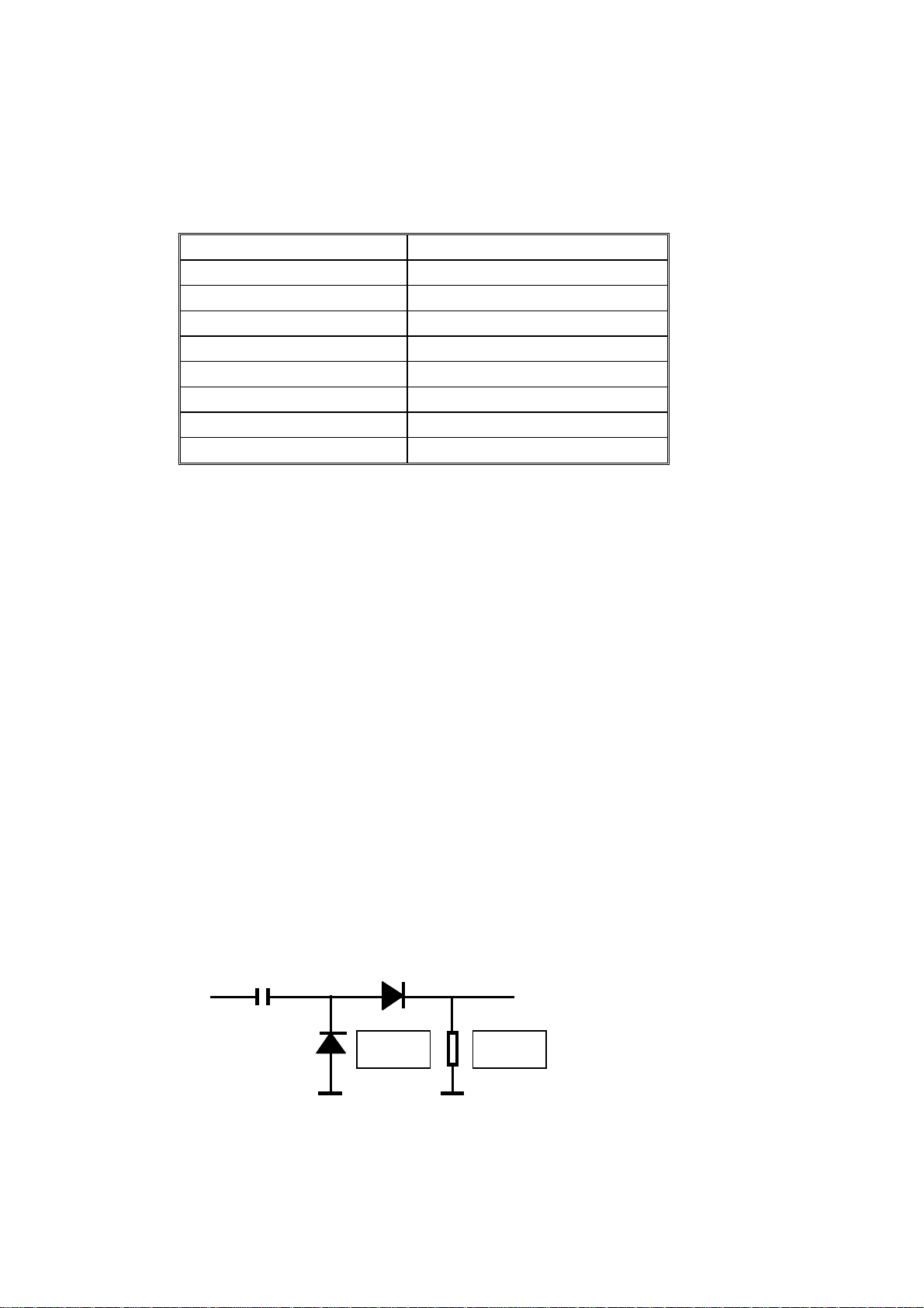
2. RF AGC adjustment
AGC Alignment Procedures:
Apply 8-scale gray signal (80dB), then adjust AGC data in D-mode to get the noise
1)
picture ( snow picture) disappear exactly. Test Pin 1 of TU101 (IF output) and
record the voltage value as V1
P-P.
<Illustrate as Picture A>
2) Apply 8-scale gray signal (80dB), and then adjust AGC data in D-mode until the
synchronization signal distortion appear exactly. Test Pin 1 of TU101 (IF output)
and record the voltage value as V2
3) Calculate the value of V
with the formula: V
P-P
<Illustrate as Picture A>
P-P.
=(V2
P-P
P-P
×V1
P-P)
1/2
Apply 8-scale gray signal (80dB), test Pin 1 of TU101 (IF output), adjust AGC data
until the voltage of Pin 1 of TU101 V
P-P
=(V2
P-P
×V1
P-P)
1/2
。
4) Test three units according to 1),2),3) steps, and record the values of AGC in three
units. Take the average value as benchmark.
Remarks:
Comparing test is necessary due to different probe of Oscilloscope and different Test
Circuit (Picture A).
1) AGC voltage value should be tested afresh, due to the type/supplier of Tuner
input
or Saw filter changed, or other related components changed.
3P f
IN60
outpu
IN60
100K
(Picture A)
Page 5

3. Screen & Focus voltage adjustment
① Apply pattern signal in normal status, enter Factory mode,press“INPUT” button
to stop vertical scan. Note:(the RC/GC/BC is preset to be 40,GD/BD is 40)
Adjust the SCRREEN switch on the flyback transformer to make a horizontal shining ②
line just visible on the screen.
Turn on the vertical output, adjust the “FOCUS” on the flyback transformer to obtain ③
the optimum focus.
4. White balance adjustment (NORMAL)
1) Apply the black and white pattern in normal status;
2) Alignment of normal color temperature
① Change Color Temperature to normal status
② Use a color analyzer to measure the black side of the screen. By changing the value
of RC, GC and BC, set the reading of the color analyzer to THOMSON standard,
x=285+
8, y=294+8.
③ Use a color analyzer to measure the white side of the screen. By changing the value
nd
dark
8,
of GD, BD, set the reading of the color analyzer to THOMSON standard, x=285+
y=294+
8.
④ Separately set the brightness and contrast from min. to max., repeat the step 2 and 3
until the reading of the color analyzer is correct.
Note: Provided the production line is equipped with the self- White balance adjusting
equipment, white balance can be adjusted automatically as following: Press “BUS OFF”
button under factory mode, the TV set will adjust automatically.
THOMSON standard:
Warm X=310+
Cool X=278+
8, Y=314+8
8, Y=282+8
Remark:
1) Provided the production line is equipped with the self- White balance adjusting
equipment, white balance of M123A chassis can be adjusted automatically as following:
Press “I2C BUS” button under factory mode, the TV set will adjust automatically.
2) Free-alignment of warm and cool temperature by presetting the value of RC-W,
GC-W, BC-W, GD-W, BD-W (for warm temperature) / RC-C,GC-C,BC-C,GD-C,BD-C(for
cool temperature ) into memory
5. Adjustment of Sub-brightness
Apply the Grey-scale/Color bar (NTSC signal) to the AV input, in normal status. Enter
factory alignment menu 5, Select BRTC to adjust the sub-brightness, until that the 2
bar of 8 level Grey scale just can be seen.
6. picture geometric adjustment
1. Apply the Philips standard testing pattern in normal status, then enter menu 3,
adjusting the following data to get the min-distortion.
HPOS6(Horizontal Center) PAR A6 (Level) TRAP6 (Trapezia)
HSIZE6(Horizontal Size) CNRT6 (To p) CNRB6 (Bottom)
Page 6
2. Apply the Philips standard testing pattern in normal status, then enter menu 3,
adjusting the following data to get the min-distortion.
HIGH6 (Height) VP60(Vertical Center)
VLIN6(Linearity) VSC6(Vertical-S Correction)
7. EHT/HEW ratio test(test with PC program):
Instruments: EHT test meter,EHT test bar(1000:1),adjustable power supply,virtual
DY( the same L value with CRT in production ).
Test means: Measure the EHT value V when Ib=0,HEW voltage value is V1(DC
voltage at 2 ends of C431).
Check means: apply PC test means,V/V1 should satisfy the requirements below:
EHT/HEW ratio
Model CRT FBT
20F420T(21K77)
J13800/1 44-14OFSN-CH3A 37-FAAT02-BAA1A
20V500T(21228)
21A31
13V420T(14001) 44-14OFSN-CH3A 37-FAAT02-BAA1A
20F512T(21185)
20V412T(21266)
14F512T(PJO559)
44-21RFLW-TS2A 37-FBAT04-CAA1A
44-21OFLN-SG6A 37-FBAT01-CAA6A
44-21RFLW-TS2A 37-FBAT04-CAA1A
44-21RFLW-TS2A 37-FBAT04-CAA1A
44-21OFLN-SG6A 37-FBAT01-CAA6A
44-15RFLP-IR4A 37-FBA003-CAA1A
EHT(0Ua)(KV) HEW(0Ua)(V)
28.5 ±2.5 21.57±1.66 1321±3%
22.5±1.5 20.6±1.66 1092±3%
26.0±2.0 21.00±1.66 1238±3%
28.5 ±2.5 21.57±1.66 1321±3%
22.5±1.5 20.6±1.66 1092±3%
28.5 ±2.5 21.57±1.66 1321±3%
26.0±2.0 21.00±1.66 1238±3%
25.5±1.5 21.70±1.66 1175±3%
RATIO
8.X rays over voltage protecting circuit test :
TV enter working mode,apply more than 26V DC voltage between two ends of C431,
the set should enter protecting mode,or check X rays protecting circuit.
Page 7

9. PS line polartities test :
Connect follow the graphic below:
DC PS
9V
- +
Sound reminder
DX 2.2k
PS socket M
TO F801
Plug the PS line onto the PS socket M, then touch any pin of F801 with the probe, the LED
DX will shine at the moment, with sound reminder, or it is disqualification.
10.PS power test (Random test) :
Instruments: Power meter.
Input signal pattern: Color bar,Sound 1KHZ ,100% modulation.
Input signal intensity: ≥60dBuv (1 Mv rms)
Test points: find the graphic below
Test means: Set the Brightness, CR to the highest, adjust the volume to make
the sound output to be 0.5W. Connect the power meter to test the
power consumption. Transfer the set to be standby, and test the
power consumption at the moment, which should meet the
requirements below:
Model Power Standby power (110V)
20F420T(21K77)
J13800/1
21A31
13V420T(14001)
20V500T(21228)
20F512T(21185)
20V412T(21266)
14F512T(PJO559)
85W ± 10% <3W
65W± 10% <3W
85W ± 10% <3W
65W± 10% <3W
75W ± 10% <3W
85W ± 10% <3W
75W ± 10% <3W
65W± 10% <3W
Page 8

11. High voltage and Ib value limit test( random test )
Instruments: High voltage meter, Ib meter.
Input signal pattern: White vertical
Input signal intensity: 60dBuv (1 Mv rms)
Test means:Connect High voltage meter and Ib meter. Test voltage of different
Ib separately, It should meet the requirements below:
Anode high voltage (Kv)
Model Ib, Ib scope
20F420T(21K77)
J13800/1
20V500T(21228)
21A31
13V420T(14001)
20F512T(21185) ……
20V412T(21266)
14F512T(PJO559)
Ib=50µA
Scope:
50µA&1000µA
….
26.0±2.0
……
…..
26.0±2.0
25.5±2.0
Value Diff.
28.4±2.5 <2
±2.0 <2
22.5
28.4±2.5 <2
±2.0 <2
22.5
28.4±2.5 <2
21”
<2
<2
<2
12.Heater voltage test ( random test )
Instruments :RMS voltage meter
Input signal pattern : Philips test graphic
Input signal intensity :1 mVrms(60dBuV)to 50 mVrms
Connect the RMS voltage meter to the 2 ends of CRT glowers,test the heater voltage of
highest CR and Brightness, It should meet:6.3±0.3Vrms
13. CCD and VOL-CHIP function test
VOL-CHIP and CCD function test,please find the service manual in detail.
14. Initialization
Under the factory mode,press“SOUND”button,the screen displays“WAIT”,
when the screen displays “OK”, the initialization finished. You can enter the next
working procedure.
15.EEPROM DATA:
Note:the items with * are adjustable, other items are not, pls do not adjust them;
Data
Model
20F512T 21185
20F420T 21K77
J13800/1
20V500T(21228)
21A31
13V420T(14001)
FAC 01
RC* GC* BC* GD* BD* HIGH5 VP50 VLIN5 VSC5 VBLK5 VCEN5
40 40 40
40 40 40
40 40 40
40 40 40
40 40 40
40 40 40
FAC 02
40 40 22
40 40 2D
40 40 20
40 40 20
40 40 2D
40 40 20 00 10 13 00 20
06 0A 09 00 17
00 10 16 00 22
00 10 13 00 20
00 10 13 00 20
00 10 16 00 22
Page 9

20V412T(21266)
14F512T(PJO559)
40 40 40
40 40 40
40 40 20
40 40 20
00 10 13 00 20
00 10 13 00 20
Page 10

Data
Model
20F512T 21185
20F420T 21K77
J13800/1
20V500T(21228)
21A31
HIGH6* VP60* VLIN6* VSC6* VBLK6 VCEN6
26 00 10 13 00 25
2E 00 10 17 00 23
21
00 10 13 00 24
26 00 10 13 00 25
2E 00 10 17 00 23
FAC 02
13V420T(14001) 21 00 10 13 00 24
20V412T(21266)
14F512T(PJO559)
26
00 10 13 00 25
26 00 10 13 00 25
FAC 03
Data
Model
20F512T 21185
20F420T 21K77
J13800/1 0F 08 08 08 06 00 02 01
20V500T(21228) 0F 08 08 08 06 00 02 01
21A31
13V420T(14001)
20V412T(21266) 0F 08 08 08 06 00 02 01
14F512T(PJO559) 0F 08 08 08 06 00 02 01
HPOS6 U BLACK V BLACKSTRAP F0SIF FREQ
10 08 08 08 06 00 02 01
0E 08 08 08 06 00 02 01
0E 08 08 08 06 00 02 01
0F 08 08 08 06 00 02 01
STRAP
HL QG
PIF FREQ
NOISE
DET
Data
Model
20F512T 21185
20F420T 21K77
J13800/1 55 0D 25 1B 7F 0E 2C 30
20V500T(21228) 7F 0D 30 1B 7F 0E 2C 30
21A31
13V420T(14001)
20V412T(21266) 7F 0D 30 1B 7F 0E 2C 30
14F512T(PJO559) 50 0D 25 1B 7F 0E 2C 30
CNTX CNTN BRTX BRTN COLX COLN TNTX TNTN
7F 10 20 1B 7F 0E 2C 30
7F 0D 30 1B 7F 0E 2C 30
7F 0D 30 1B 7F 0E 2C 30
55 0D 25 1B 7F 0E 2C 30
FAC 04
Data
Model
20F512T 21185
20F420T 21K77
BRTC* COLC COLP SCOL SCNT CNTC TNTCT TNTCV
48 38 00 07 0F 3A 45 45
3C 38 00 07 0F 3A 58 3D
FAC 05
Page 11

J13800/1 3C 38 00 07 0F 3A 58 3D
20V500T(21228) 3C 38 00 07 0F 3A 58 3D
21A31
13V420T(14001)
20V412T(21266) 3C 38 00 07 0F 3A 58 3D
14F512T(PJO559) 3C 38 00 07 0F 29 58 3D
3C 38 00 07 0F 3A 58 3D
3C 38 00 07 0F 3A 58 3D
Data
Model
20F512T 21185
20F420T 21K77
13800/1
20V500T(21228) 1B 1B 1B 1B 07 1A 1A
21A31
13V420T(14001)
20V412T(21266) 1B 1B 1B 1B 07 1A 1A
14F512T(PJO559) 1B 1B 1B 1B 07 1A 1A
ST3 SV3 SV4 SVD ASSH SHPX SHPN
1B 1B 1B 1B 07 1A 1A
1B 1B 1B 1B 07 1A 1A
1B 1B 1B 1B 07 1A 1A
1B 1B 1B 1B 07 1A 1A
1B 1B 1B 1B 07 1A 1A
FAC 06
Page 12

Data
Model
20F512T 21185
20F420T 21K77
J13800/1 60 00 80 37 C4 C1 09 FF
20V500T(21228) 60 30 80 37 C4 81 09 FF
21A31
13V420T(14001)
20V412T(21266) 60 30 80 37 C4 81 09 FF
14F512T(PJO559) 70 30 80 37 C2 81 09 FF
MOD1 MOD2 MOD3 OPT OPTM1 OPTM2 HDCNT HSTOP
70 30 80 37 C2 81 09 FF
60 30 80 37 C4 C1 09 FF
60 30 80 37 C2 C1 09 FF
60 10 80 37 C4 C1 09 FF
FAC 07
Data
Model
20F512T 21185
‘20F420T 21K77
J13800/1 25 00 21 53 4A 65 1F 16
20V500T(21228) 25 00 21 53 4A 65 1F 16
21A31
13V420T(14001)
20V412T(21266) 25 00 21 53 4A 65 1F 16
14F512T(PJO559) 25 00 21 53 4A 65 1F 16
RF AGC* BRTS OSD OSDF CCD OSD CCD OSDF TXCN RGCN
25 00 21 53 4A 65 1F 16
25 00 21 53 4A 65 1F 16
25 00 21 53 4A 65 1F 16
25 00 21 53 4A 65 1F 16
FAC 08
Data
Model
20F512T 21185
20F420T 21K77
J13800/1 0D 15 27 41 51 5F 6C 6F 32
20V500T(21228) 0D 15 27 41 51 5F 6C 6F 32
21A31
13V420T(14001)
20V412T(21266) 0D 15 27 41 51 5F 6C 6F 32
14F512T(PJO559) 35 48 53 60 66 68 6A 6D 32
V01
35 48 53 60 66 68 6A 6D 32
0D 15 27 41 51 5F 6C 6F 32
V05
35 48 53 60 66 68 6A 6D 32
0D 15 27 41 51 5F 6C 6F 32
V10 V25 V50 V75 V90 V100 VOLMAX
FAC 09
Data
Model
20F512T 21185
20F420T 21K77
CURTCEN VOLX PWTM
A5 7F 08
A5 7F 08
FAC 10
MODE4 MODE5 MODE6 MODE7 MODE8 MODE9
22 0B 1E 47 2D CA
22 0B 1E 47 2D CA
Page 13

J13800/1 A5 7F 08 22 0B 1E 47 2D 02
20V500T(21228) A5 7F 08 22 0B 1E 47 2D CA
21A31
13V420T(14001)
20V412T(21266) A5 7F 08 22 0B 1E 47 2D CA
14F512T(PJO559) A5 7F 08 22 0B 1E 47 2D CA
A5 7F 08
A5 7F 08
22 0B 1E 47 2D CA
22 0B 1E 47 2D C2
Data
Model
20F512T 21185
20F420T 21K77
J13800/1 06 06 02 00 0A 0A 03
20V500T(21228) 06 06 02 00 0A 0A 03
21A31
13V420T(14001)
20V412T(21266) 06 06 02 00 0A 0A 03
14F512T(PJO559) 06 06 02 00 0A 0A 03
CON1 CON2 CON3 STSADJ ALI 1 ALI 2 ALI3
06 06 02 00 0A 0A 03
06 06 02 00 0A 0A 03
06 06 02 00 0A 0A 03
06 06 02 00 0A 0A 03
FAC 11
Page 14

Data
Model
20F512T 21185
20F420T 21K77
J13800/1 10 10 20 64 28 18 22 10
20V500T(21228) 10 10 20 64 28 18 22 10
21A31
13V420T(14001)
20V412T(21266) 10 10 20 64 28 18 22 10
14F512T(PJO559) 10 10 20 64 28 18 22 10
SVM SVM1 OSD2 OSDF2 PYNX PYNN PYXS PYNS
10 10 20 64 28 18 22 10
10 10 20 64 28 18 22 10
10 10 20 64 28 18 22 10
10 10 20 64 28 18 22 10
FAC 12
Data
Model
20F512T 21185
20F420T 21K77
J13800/1 04 03 03 27 14 82 0C
20V500T(21228) 04 03 03 27 14 82 0C
21A31
13V420T(14001)
20V412T(21266) 04 03 03 27 14 82 0C
14F512T(PJO559) 04 03 03 27 14 82 0C
CLTM CLVO CLVS ABL DCBS FLG0 FLG1
04 03 03 27 14 82 0C
04 03 03 27 14 82 0C
04 03 03 27 14 82 0C
04 03 03 27 14 82 0C
FAC 13
Data
Model
20F512T 21185
20F420T 21K77
J13800/1 09 1C 01 08 1A 80 80 00 00 00 00 00
20V500T(21228) 09 1C 01 08 1A 80 80 -- -- -- -- --
21A31 09 1C 01 08 1A 80 80 00 00 00 00 00
13V420T(14001)
20V412T(21266) 09 1C 01 08 1A 80 80 -- -- -- -- -14F512T(PJO559) 09 1C 01 08 1A 80 80 -- -- -- -- --
HAFC AGCC NOIS ONTM NSHP PVLVL PLMT RC-C GC-C BC-C GD-C BD-C
09 1C 01 08 1A 80 80 -- -- -- -- --
09 1C 01 08 1A 80 80 00 00 00 00 00
09 1C 01 08 1A 80 80 00 00 00 00 00
FAC 14
FAC 15
Data
Model
20F512T 21185
20F420T 21K77
J13800/1 00 00 00 00 00 00 00 32 32 5A 32
20V500T(21228) -- -- -- -- -- -- -- 32 32 5A 32
RC-W GC-W BC-W GD-W BD-W YUVGC YUVBC D-COL D-BRI D-CON D-SHP
-- -- -- -- -- -- -- 32 32 5A 32
00 00 00 00 00 00 00 32 32 5A 32
FAC 16
FAC 17
Page 15

21A31 00 00 00 00 00 00 00 32 32 5A 32
13V420T(14001)
20V412T(21266) -- -- -- -- -- -- -- 32 32 5A 32
14F512T(PJO559) -- -- -- -- -- -- -- 32 32 5A 32
00 00 00 00 00 00 00 32 32 5A 32
Data
Model
20F512T 21185
20F420T 21K77
J13800/1 32 32 32 32 32 32 1E 32
20V500T(21228) 32 32 32 32 32 32 1E 32
21A31 32 32 32 32 32 32 1E 32
13V420T(14001)
20V412T(21266) 32 32 32 32 32 32 1E 32
14F512T(PJO559) 32 32 32 32 32 32 1E 32
S-COL S-BRI S-CON S-SHP M-COL M-BRI M-CON M-SHP
32 32 32 32 32 32 1E 32
32 32 32 32 32 32 1E 32
32 32 32 32 32 32 1E 32
FAC 18 FAC 19
Data
Model
20F512T 21185
20F420T 21K77
J13800/1 173 407 01 02 08 06 05 00 00
20V500T(21228) 173 407 01 02 08 06 05 00 00
21A31
13V420T(14001)
20V412T(21266) 173 407 01 02 08 06 05 00 00
14F512T(PJO559) 173 407 01 02 08 06 05 00 00
SEG-POINT1 SEG-POINT2DATA-VLDATA-VHDATA-UF SPE-POS1 SPE-DATA1 SENSI-ONSENSI-OFF
173 407 01 02 08 06 05 00 00
173 407 01 02 08 06 05 00 00
173 407 01 02 08 06 05 00 00
173 407 01 02 08 06 05 00 00
FAC 20
Data
Model
20F512T 21185
20F420T 21K77
J13800/1 2D 4A 38 3E 19 2C
20V500T(21228) 2D 4A 38 3E 19 2C
21A31
13V420T(14001)
20V412T(21266) 2D 4A 38 3E 19 2C
14F512T(PJO559) 2D 4A 38 3E 19 2C
THEATER-BAS
2D 4A 38 3E 19 2C
2D 4A 38 3E 19 2C
2D 4A 38 3E 19 2C
2D 4A 38 3E 19 2C
THEATER-TRE
CONCERT-BASCONCERT-TRE BROCAST-BAS BROCAST-TRE
FAC 21
FAC 22
Page 16

Model
20F512T 21185
20F420T 21K77
J13800/1 03 2A 75 2D 48
20V500T(21228) 03 2A 75 2D 48
21A31
13V420T(14001)
20V412T(21266) 03 2A 75 2D 48
14F512T(PJO559) 03 2A 75 2D 48
VOL_MAI
03 2A 75 2D 48
03 2A 75 2D 48
03 2A 75 2D 48
03 2A 75 2D 48
GATE VOL-OUT AV GAIN OPTM3
Data
Model
20F512T 21185
20F420T 21K77
J13800/1 30 06 00 02 00 00
20V500T(21228) 30 06 00 02 00 00
21A31
13V420T(14001)
20V412T(21266) 30 06 00 02 00 00
14F512T(PJO559) 30 06 00 02 00 00
G2_FLAG00 G2_FLAG01 G2_FLAG02 G2_FLAG03 G2_FLAG04 G2_FLAG05
30 06 00 02 00 00
30 06 00 02 00 00
30 06 00 02 00 00
30 06 00 02 00 00
FAC 25
Page 17

Ⅲ. CDRH Document :
1. Testing for EHT and HEW
Model CRT FBT
20F420T(21K77)
J13800/1 44-14OFSN-CH3A 37-FAAT02-BAA1A
20V500T(21228)
21A31
13V420T(14001)
20F512T(21185)
20V412T(21266) 44-21OFLN-SG6A 37-FBAT01-CAA6A
14F512T(PJO559) 44-15RFLP-IR4A 37-FBA003-CAA1A
44-21RFLW-TS2A 37-FBAT04-CAA1A
44-21OFLN-SG6A 37-FBAT01-CAA6A
44-21RFLW-TS2A 37-FBAT04-CAA1A
44-14OFSN-CH3A 37-FAAT02-BAA1A
44-21RFLW-TS2A 37-FBAT04-CAA1A
2. Value of Sample Register in X-ray protection circuit
Model BOM CRT Designator value
20F420T(21K77)
J13800/1 03-EV13AGP-TU00/1 44-14OFSN-CH3A
20V500T(21228)
21A31
13V420T(14001)
20F512T(21185)
20V412T(21266) 03-D266AGP-TU23W 44-21OFLN-SG6A
14F512T(PJO559) 03-F559AGP-TU23W 44-15RFLP-IR4A
03-DK77AGP-TU23 44-21RFLW-TS2A
03-D228AGP-TU23 44—21OFLN-SG6A
03-DA31AGP-TU26W 44-21RFLW-TS2A
03-E001AGP-TU23W 44-14OFSN-CH3A
03-D185AG-TU60 44-21RFLW-TS2A
EHT(0Ua)
(KV)
28.5 ±2.5 21.57±1.66 1321±3%
22.5±1.5 20.60±1.66 1092±3%
26.0±1.5 21.00±1.66 1238±3%
28.5 ±2.5 21.57±1.66 1321±3%
22.5±1.5 20.60±1.66 1092±3%
28.5 ±2.5 21.57±1.66 1321±3%
26.0±1.5 21.00±1.66 1238±3%
25.5±1.5 21.70±1.66 1175±3%
HEW(0Ua)
(V)
RATIO
R433/R436 470Ω/120Ω
R433/R436 470Ω/100Ω
R433/R436 680Ω/100Ω
R433/R436 470Ω/120Ω
R433/R436 470Ω/100Ω
R433/R436 470Ω/120Ω
R433/R436 680Ω/100Ω
R433/R436 470Ω/82Ω
3. Test of X-ray protection circuit
( X-ray protection circuit will not work with normal voltage, or it does work with over-load voltage)
Model BOM CRT Designator
20F420T(21K77)
J13800/1 03-EV13AGP-TU00/1 44-14OFSN-CH3A
20V500T(21228)
21A31
13V420T(14001)
20F512T(21185)
20V412T(21266) 03-D266AGP-TU23W 44-21OFLN-SG6A
14F512T(PJO559) 03-F559AGP-TU23W 44-15RFLP-IR4A
03-DK77AGP-TU23 44-21RFLW-TS2A
03-D228AGP-TU23 44-21OFLN-SG6A
03-DA31AGP-TU26W 44-21RFLW-TS2A
03-E001AGP-TU23W 44-14OFSN-CH3A
03-D185AG-TU60 44-21RFLW-TS2A
C431
C431
C431
C431
C431
C431
C431
C431
Normal
Voltage
21±1.0
20.6±1.0
±1.0
21
21±1.0
20.6±1.0
21±1.0
±1.0
21
±1.0
21.7
over-load
voltage
>26V
>26V
>26V
>26V
>26V
>26V
>26V
>26V
 Loading...