

ALESS AL3201SCR Datasheet
Alesis Semiconductor
DS3201-08 02 12555 Jefferson Blvd., Sui te 285
Los Angeles, CA 90066
Phone (310) 301-0780 Fax (310) 306-1551 www.alesis-semi.com
We make the parts that set creative people free
General Description
The AL3201 (SCR, or Single Chip Reverb)
is a one chip reverb solution that is
compact, easy to use, and yet quite
powerful. Built-in DRAM eliminates the
need for wide bus c onnections to external
RAM, and the choice of built-in programs
and a user programmable RAM allows
instant usability or custom program
design.
Features
16 internal ROM programs consisting
of halls, rooms, plates, delays, chorus,
flange, vocal cancel, and rotary
speaker emulation.
Serially programmable SRAM (Writable
Control Store – WCS) for program
development or dynamically changing
programs
Programs run at 128 instructions per
word clock. (6 MIPS @ 48kHz sampling frequency.)
32k location DRAM provides over 0.6 8s
of delay at 48kHz sampling frequency.
Internal crystal oscillator circuit
eliminates need for discrete external
passive components.
Internal voltage regulators allow opera-
tion at both 5V an d 3.3V V
DD
.
Internal 1000pF bypass capacitor to
reduce voltage swings at the rails.
Applications
Personal stereos with reverb functions.
Extremely portable guitar effects boxes.
Karaoke machines utilizing the vocal cancel program.
Hardware reverb ef fects for computer so und cards.
Ambience settings for car stereos.
DigOut
Int/Ext
XtalIn
XtalOut
Prog0/SData
Prog1/SClk
Prog2
Prog3
DigIn
Bypass
Gnd
Reset
SysClk
BitClk
WordClk
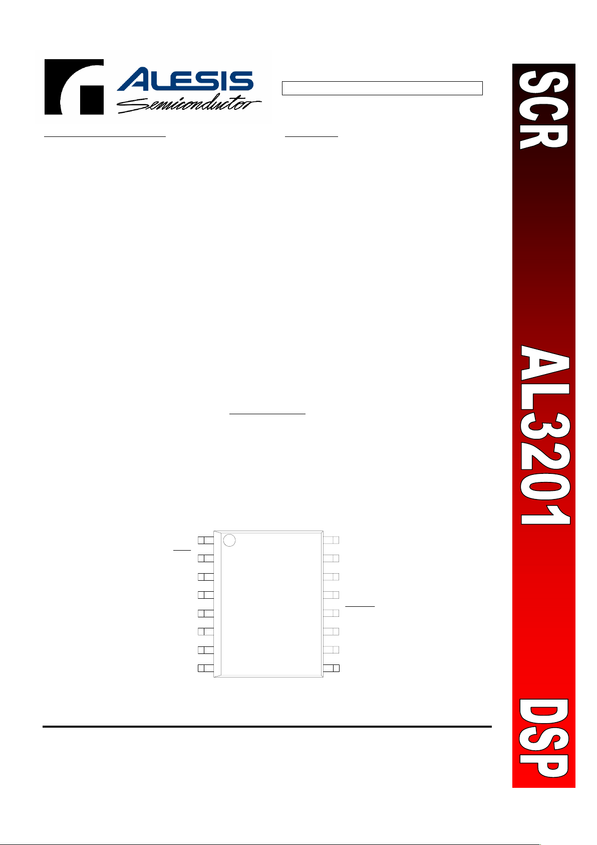
16 pin SOIC
300 mils wide
1
8
1
6
9
V
DD
A
L
3
2
0
1
S
C
R
Alesis Semiconductor
DS3201-08 02 12555 Jefferson Blvd., Sui te 285
Los Angeles, CA 90066
Phone (310) 301-0780 Fax (310) 306-1551 www.alesis-semi.com
-
2 -
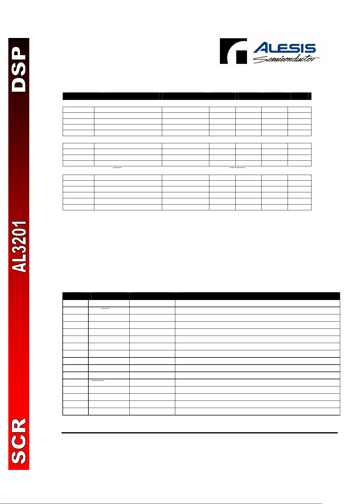
Electrical Characteristics and Operating Conditions
Parameter Description Condition Min Typ Max Units
Electrical Characteristics and Operating Conditions
VDD Supply Voltage 3.0/4.5 3.3/5.0 3.6/5.5 V
IDD Supply Current : SCR 6/9 7/10 8/11 mA
Gnd Ground Note 3 - 0.0 - V
FS Sample rate 24
1
48 50
1
kHz
Temp
Temperature
0 25 70
°C
Outputs (DigOut, SysClk, BitClk, WordClk)
VOH Logical “1” output voltage Unloaded 0.9 VDD VDD - V
VOL Logical “0” output voltage Unloaded - 0 0.05 VDD V
IOH Logical “1” output current VDD=5V VO=4.5V - - -8.0 mA
IOL Logical “0” output current VDD=5V VO=0.4V - - 8.0 mA
_______________ __________________________
Inputs (DigIn, Int/Ext, Prog0/Sdata, Prog1/SClk, Prog2, Prog3, Reset) Notes 2,4
VIH Logical “1” input voltage 2.5 - VDD V
VIL Logical “0” input voltage 0 - 0.5 V
IIH Logical “1” input current
V
DD=VIH
=5V
- - 2
µA
IIL Logical “0” input current
No pullup pin
- - 2
µA
I
ILP
Logical “0” input current
Pullup pin, Vin=0
83 167 333
µA
CIN Input Capacitance - 2.0 - pF
Note:
1. Changing the sample rate (by changing the crystal frequency) will change the maximum delay
available through the DRAM proportionally. Low sample rates require mor e refresh instructio ns.
2. XtalIn, XtalOut are special pins designed to be connected to a crystal. XtalOut is a relatively weak pin
(about 0.2 mA) and should not be used to drive external circuits. Instead of using a crystal, XtalIn
may be driven by a standard V
DD
to Gnd logic signal, but the logic levels are n ot specified.
3. All other voltages are relative to Gnd.
4. Bypass (pin 14) must never exceed 3.6V
Pin Descriptions: AL3201 SCR (*: Pullup to V
DD
via nominal internal 30kΩ resistor)
Pin # Name Pin Type Description
1 DigOut Output Digital serial output for stereo DAC.
2
______________
Int/Ext
Input* Internal/extern al program sel ection. 1:Internal, 0: External.
3 XtalIn Input 12.288MHz crystal input.
4 XtalOut Output 12.288MHz crystal output.
5 Prog0/SData Bidirectional* Internal program select 0 / serial i n terface data lin e.
6 Prog1/SClk Input* Internal program select 1 / serial interface clock line.
7 Prog2 Input* Internal progr a m select 2.
8 Prog3 Input* Internal progr a m select 3.
9 WordClk Output Word clock output.
10 BitClk Output Bit clock output.
11 SysClk Output System clock output.
12
________________ _____
Reset
Input Active low reset.
13 Gnd Ground Ground connection.
14 Bypass Bidirectional
Connect 0.1µF bypass capacitor to Gnd for internal +3.3V regulator.
15 V
DD
Power
+5V/+3.3V V
DD
power pin. Connect 0.1µF capacitor to Gn d.
16 DigIn Input Digital serial input fr om stereo ADC.
Alesis Semiconductor
DS3201-08 02 12555 Jefferson Blvd., Sui te 285
Los Angeles, CA 90066
Phone (310) 301-0780 Fax (310) 306-1551 www.alesis-semi.com
-
3 -
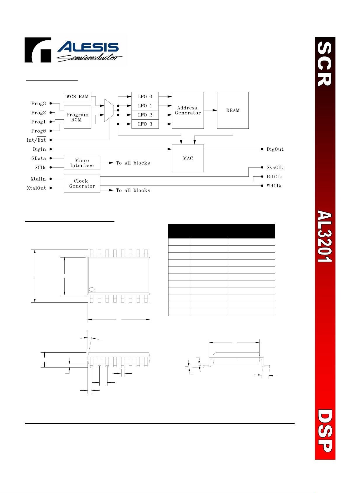
Block Diagram
Mechanical Specification
1
8
916
E
D
F
H
G
L
K
7° nom
BC
4° nom
J
A
Dimensions (T ypical)
Inches Millimeters
A
.406”
10.31
B .295” 7.49
C .407” 10.34
D .100” 2.50
E .008” 0.20
F .025” 0.64
G .050” 1.27
H .017” 0.42
J .011” 0.27
K .340” 8.66
L .033” 0.83
Notes:
1) Dimension “A” do es not include mo ld
flash, protrusions or gate burrs.
 Loading...