


not permitted
Table of Content
1. GENERALITIES ............................................................................................................... 2
1.1 I
1.2 S
1.3 E
1.4 T
1.5 R
NTRODUCTION
............................................................................................................................................. 2
1.1.1 Overview .................................................................................................................................................. 2
1.1.2 Aim of the document ................................................................................................................................. 3
ERVICES PROVIDED BY THE FEATURE OR EQUIPMENT
XTERNAL INTERFACES
ERMINOLOGY / ABBREVIATIONS
ELATED DOCUMENTS
................................................................................................................................ 3
................................................................................................................. 5
................................................................................................................................. 6
................................................................................. 3
2. GENERAL REQUIREMENTS ........................................................................................ 7
2.1 F
2.2 S
2.3 E
EATURES
TANDARDS
..................................................................................................................................................... 7
.................................................................................................................................................. 7
2.2.1 BT related certification ............................................................................................................................ 7
NVIRONMENTAL REQUIREMENTS
................................................................................................................ 8
3. GENERAL DESCRIPTION ............................................................................................. 9
3.1 BT
3.2 BT
3.3 M
3.4 S
FUNCTION GLOBAL LOGICAL BLOC DIAGRAM
DAUGHTER BOARD BLOC DIAGRAM
ECHANICAL ASPECTS AND INTEGRATION
PECIFICATION
............................................................................................................................................ 11
......................................................................................................... 9
................................................................................................. 10
......................................................................................... 9
4. DETAILED TECHNICAL DESCRIPTION .................................................................. 12
4.1 E
4.2 R
4.3 L
4.4 S
4.5 C
LECTRONIC
............................................................................................................................................... 12
4.1.1 BT chip solution to be implemented ....................................................................................................... 12
4.1.2 Schematic ............................................................................................................................................... 13
ADIOFREQUENCY
...................................................................................................................................... 14
4.2.1 Antenna choice ....................................................................................................................................... 14
4.2.2 Immunity to external spurious and interferences ................................................................................... 15
4.2.3 Quality of supply .................................................................................................................................... 15
AYOUT
...................................................................................................................................................... 16
4.3.1 BTDB layout ........................................................................................................................................... 16
4.3.2 Place requirements of BTDB on mainboard .......................................................................................... 16
OFTWARE
ERTIFICATION
.................................................................................................................................................. 16
........................................................................................................................................... 17
4.5.1 General aspects on the “module” concept ............................................................................................ 17
5. THERMAL MANAGEMENT ........................................................................................ 18
6. RELIABILITY ................................................................................................................ 18
7. INDUSTRIAL CONSIDERATIONS .............................................................................. 18
7.1 M
7.2 R
7.3 T
7.4 M
ANUFACTURING
EQUIREMENTS
ESTABILITY
....................................................................................................................................... 18
.......................................................................................................................................... 18
............................................................................................................................................... 18
7.3.1 Testpoints................................................................................................................................................ 18
7.3.2 Test strategy ........................................................................................................................................... 19
7.3.3 Test method ............................................................................................................................................. 20
ECHANICAL ASSEMBLY / INDUSTRIAL FEASIBILITY
.................................................................................. 23
7.4.1 Board outline .......................................................................................................................................... 23
7.4.2 Board technology ................................................................................................................................... 23
7.4.3 Connections ............................................................................................................................................ 24
7.4.4 Mounting on the main board .................................................................................................................. 24
7.4.5 Shielding Mounting ................................................................................................................................ 26

not permitted
Generalities
1.1 Introduction
1.1.1 Overview
The main objectives for this board, discussed also with the marketing are:
• Get lowest cost solution to enable BT for a maximum of IP terminals
• Enable new usages like
o The phone is seen as a carkit for a smartphone
o The phone can exchange phonebook with a smartphone
o The phone can support tags through BT Low Energy
• From R&D point of view:
o The board must be small enough to be integrated easily into our ID.
o The board must integrate the antenna to avoid a re-certification for each phone
which would use it.
For this project, a pre-study has been done. See reference [1].
The choice is to do a daughter board with the chip CC2564C from Texas Instruments, with an
integrated antenna on the layout (Printed antenna).
This device complies with part 15 of the FCC Rules. Operation is subject to the following two
conditions:
(1) This device may not cause harmful interference, and
(2) this device must accept any interference received, including interference that may cause
undesired operation.
Please note that changes or modifications not expressly approved by the party responsible for
compliance could void the user’s authority to operate the equipment.
Note: This equipment has been tested and found to comply with the limits for a Class B digital
device, pursuant to part 15 of the FCC Rules. These limits are designed to provide reasonable
protection against harmful interference in a residential installation. This equipment generates, uses
and can radiate radio frequency energy and, if not installed and used in accordance with the
instructions, may cause harmful interference to radio communications. However, there is no
guarantee that interference will not occur in a particular installation. If this equipment does cause
harmful interference to radio or television reception, which can be determined by turning the
equipment off and on, the user is encouraged to try to correct the interference by one or more of the
following measures:
—Reorient or relocate the receiving antenna.
—Increase the separation between the equipment and receiver.

not permitted
—Connect the equipment into an outlet on a circuit different from that to which the receiver is
connected.
—Consult the dealer or an experienced radio/TV technician for help.
This device complies with Industry Canada’s licence-exempt RSSs. Operation is subject to the
following two conditions:
(1) This device may not cause interference; and
(2) This device must accept any interference, including interference that may cause undesired
operation of the device.
Le présent appareil est conforme aux CNR d'Industrie Canada applicables aux appareils radio
exempts de licence. L'exploitation est autorisée aux deux conditions suivantes:
(1) l'appareil ne doit pas produire de brouillage;
(2)l'utilisateur de l'appareil doit accepter tout brouillage radioélectrique subi, même si le brouillage
est susceptible d'en compromettre le fonctionnement.
CAN ICES-3 (B)/NMB-3(B)
1.1.2 Aim of the document
A pre-study has been done, in order to define the best choices for the whole solution, going from
antenna to the BT management software in the phone.
This document is intended to give all the technical inputs in order to make a BT daughter board
which will be used on the Alcatel-Lucent IP Phones.
A first step will be to use it on 8068s and 8078s, but we should care to make it possible to be used
also on nextgen phones and other projects.
1.2 Services provided by the feature or equipment
The BTDB will give a BT4.2 connectivity to the product where it is mounted into. The main reasons
of this daughter board are to have:
• A common function usable on several phones without the need of RF expertise and full
BT qualification
• A cost effective solution
1.3 External Interfaces
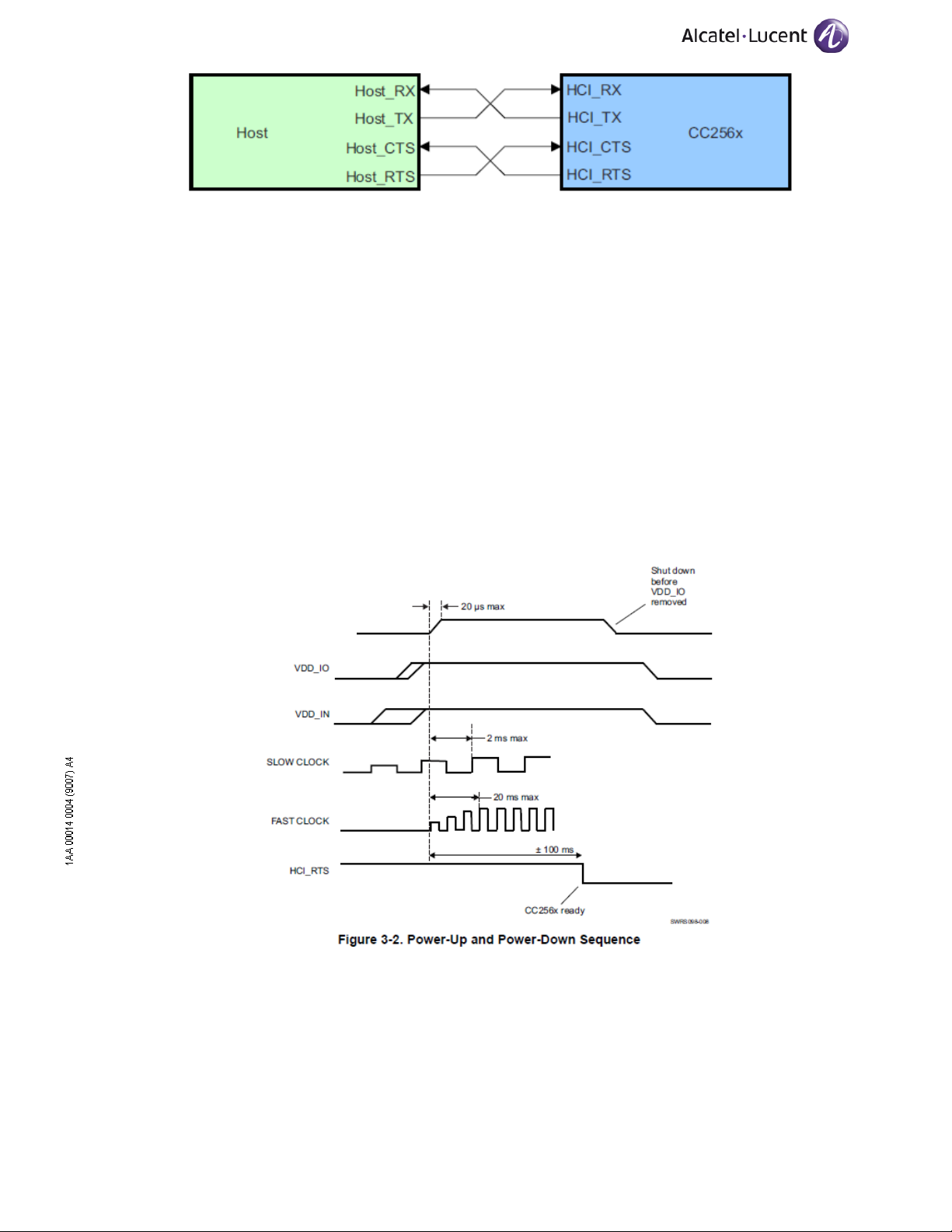
The interface signals are listed hereafter:
not permitted
Pin N° Name Function Type Voltage
5 GND
Keep feet on the ground.
Power
0V
6 HCI_RX
HS UART Receive up to
4Mbps
I
/PU 1.8V
1 GND
Keep feet on the ground. Power 0V
2 VDD_IO Direct path supply for 1.8V I/O pads. Power 1.8V
3 GND Keep feet on the ground. Power 0V
4 SLOW_CLK 32.768KHz +/- 250ppm I 1.8V
7 TX_DBG TI internal debug messages. Not used. O /PU 1.8V
8 HCI_CTS
HS UART flow control: data from BTDB to
Host allowed when low
I /PU 1.8V
9 GND Keep feet on the ground. Power 0V
10 GND Keep feet on the ground. Power 0V
11 HCI_RTS
HS UART flow control: data from host to
BTDB allowed when low
O /PU* 1.8V
12 HCI_TX HS UART Transmit up to 4Mbps O/PU* 1.8V
13 GND Keep feet on the ground. Power 0V
14 PCM_SYNC Frame synchro for audio data I/O /PD 1.8V
15 PCM_CLK Clock for audio data I/O /PD 1.8V
16 PCM_OUT Output of audio data. Maybe in tristate O /PD 1.8V
17 PCM_IN Input of audio data I 1.8V
18-23 GND
Keep feet on the ground. Power 0V
Disables BT chip when low (Pull down)
24 ENABLE
and performs internal reset of CC2564.
I /PD 1.8V
Minimum low state duration: 5ms
25 GND Keep feet on the ground. Power 0V
26 VDD_IN General supply I 2.2V-4.8V
27 GND
Keep feet on the ground. Power 0V
PU* : Pull-Up enabled only during ShutDown and DeepSleep phases (.
These correspond to the metal cut-holes. See chapter 7.4.3.
The VDD_IN pin can accept 2.2V to 4.8V. Typical value is 2.5V or 3.3V, but this depends on the
motherboard.
Check the CC2564C datasheet for more information.
The UART has by default the following characteristics (can be reprogrammed to up to 4Mbps)
not permitted
Check the CC2564C datasheet for more information.
This cabling supposes that the Host is in DTE mode. In case of DCE host, RTS and CTS are
straight, and not crossed.
CAUTION:
Only the following interfaces are fail safe (can stand an applied voltage when the device interface, or
the device is not powered (VDDio or VDDin not provided):
AUD_FSYNC, AUD_CLK, AUD_IN, AUD_OUT, SLOW_CLK
This means that the motherboard must not apply a voltage on HCI_RX, HCI_TX, HCI_CTS or
HCI_RTS pins before the VDDio is supplied. Even when VDDio is present, it is not allowed to
ENABLE the chip if VDDin is not present. See specification of CC2564 for more details.
The SLOW_CLK source must be stable within 2ms after the ENABLE LOW to HIGH transition.
ENABLE
Note: FAST CLOCK must be stable within 20ms of nSHUTD(ENABLE) going high. But according to TI FAE’s feedback,
the 20ms limit only applies to TCXO. Crystal is used in BTDB, which doesn’t need to follow the 20ms limit.
1.4 Terminology / Abbreviations
BTDB: BlueTooth Daughter Board
BT: BlueTooth
not permitted
LE: Low Energy
1.5 Related Documents
Alcatel documents
[1] Bluetooth: Pre-study of a low cost solution for
BT in Desktop Phones
[2] 8088 Hardware external specification 3AK_29000_0080_EDZZA
[3] ESD CSBU R&D - PB Design/Layout rules 8AL 51074 0003 DSZZA
[4] NOE3G INDUSTRIAL REQUIREMENTS
External documents
[5] All TI documents for CC2564 (upload) 3AK_29_CC256X_BLUETOOTH_02278
[6]
Document Reference number
3AK_29000_0041_BEZZA
3BN 69030 1403 MCASA

not permitted
2. General Requirements
2.1 Features
The board must provide the following features:
• Give dual mode BT connectivity (Classic & Low Energy), so BT4.1
• Integrate the antenna, done with copper tracks on the PCB
• Interface to the motherboard with UART and PCM, USB not required.
• Permit a very low cost solution.
• Give ease of re-use for other products (simple process, no RF expertise).
2.2 Standards
2.2.1 BT related certification
On the Bluetooth.org website, the existing certifications of BT solutions are listed.
The certification strategy will be as follows:
• Make a certification for the board, with embedded low part of the BT stack, and antenna
• Make a product certification, where the BTDB is in the Phone. Here we can take benefit
of the module certification
• Following the first product certification (ex: NOE3GEE), the next products which use the
BTDB will need minimum or no certification, on condition that the used upper BT stack (in
host processor) is the same as the one of NOE3GEE.
It is necessary to make a BT qualification for the BTDB with its antenna.
This will qualify:
• The hardware, radio parts
• The Lower part of the BT stack (below HCI interface) located in the BT chip
• The Upper part of the BT stack, which runs on the Host processor.
This is why, if we re-use this board, a big part of the certification does not need to be done.
See chapter 4.5.1 for discussion about the “module” aspect for BT certification.

not permitted
2.3 Environmental requirements
These are the same as for the terminal for which this board is intended. The tests are made on the
daughter board mounted in a final product, so they are part of the product qualification.
This BTDB board cannot be co-located with other transmitters. If mount this board on final product,
Should add FCC ID and IC information in the product label (FCC ID: OL3BTMOD02, IC: 1737DBTMOD02).
For a host manufacture’s using a certified modular, if (1) the module’s FCC ID is not visible when
installed in the host, or (2) if the host is marketed so that end users do not have straightforward
commonly used methods for access to remove the module so that the FCC ID of the module is
visible; then an additional permanent label referring to the enclosed module: “Contains Transmitter
Module FCC ID: OL3BTMOD02, IC: 1737D-BTMOD02” or “Contains FCC ID: OL3BTMOD02,
Contains IC: 1737D-BTMOD02” must be used. The host OEM user manual must also contain clear
instructions on how end users can find and/or access the module and the FCC ID.
This equipment complies with radio frequency exposure limits set forth by the Innovation, Science
and Economic Development Canada for an uncontrolled environment.
This equipment should be installed and operated with a minimum distance of 15mm between the
device and the user or bystanders.
This device must not be co-located or operating in conjunction with any other antenna or transmitter.
Cet équipement est conforme aux limites d'exposition aux radiofréquences définies par la
Innovation, Sciences et Développement économique Canada pour un environnement non contrôlé.
Cet équipement doit être installé et utilisé avec un minimum de 15mm de distance entre le dispositif
et l'utilisateur ou des tiers.
Ce dispositif ne doit pas être utilisé à proximité d’une autre antenne ou d’un autre émetteur.
For details see for example the Smart Deskphone 8088 HW external specification (see ref [2])

not permitted
3. General Description
Crystal
Bandpass
filter
2.4GHz Antenna
32.768KHz
1.8V
< 20ppm
2.2V-4.8V
DC/DC
1.8V
UART
PCM
GPIO
Daughter Board PC
B
3.1 BT function global logical bloc diagram
3.2 BT daughter board bloc diagram
VDD Vdd I/O LDO_out
UART
PCM/I2S
SlowClock
Enable TI CC2564C
26MHz

not permitted
No copper
under
L
L
/3
The CC2564C communicates with a standard HCI through the UART interface.
Here is a representation of the lower part of the stack, which is inside the CC2564C:
This means that the upper part of the stack must be hosted in the mother board cpu.
3.3 Mechanical aspects and integration
This board will be mounted on a IP Phone CPU board or BT handset CPU board.
For radiofrequency propagation reasons, the antenna area must not cover any copper plane.
For industrial reasons, the board must lay on the CPU board on at least 2/3 of it’s surface.
Examples of implementation follow:
= +
= +
CPU PCB
CPU PCB
Another alternative, best is:
antenna
Copper OK
= +
max
CPU PCB
CPU PCB

not permitted
Parameter
Value
Host interface
3.4 Specification
Standard support Bluetooth 2.1 + EDR, BLE 4.2
HCI UART
V
Min, Max 1.7 Volts, 4.8 Volts
BAT
V
Min, Max 1.62 Volts, 1.92 Volts
DD_IO
Temperature range (board) -5 to +65°C
Frequency range 2402 MHz to 2480 MHz
Transmit power GFSK, and
+4 dBm typ +6dBm max
EDR
Transmit power BLE -6dBm typ -4dBm max
RX Sensitivity BR -91.5 dBm, GFSK at 0.1%
Max
BER
RX Sensitivity EDR -81 dBm, 8DPSK at 0.01%
Max
BER
RX Sensitivity BLE -93 dBm, PER=30.8% Max
Full throughput current 42 mA, GFSK or EDR Max
SCO link HV3 15 mA Max
Idle current BR and EDR 5 mA Max
BLE Scanning 310 uA Max
BLE Advertising 150 uA Max
Shutdown current 10 uA Max

not permitted
4. Detailed Technical Description
4.1 Electronic
4.1.1 BT chip solution to be implemented
The chosen chip to implement BT4.2 compliant connectivity is the Texas Instruments CC2564C
chip.
This is a dual mode (Classic + Low Energy) one chip solution.
This chip comes in several versions:
• Version A (CC2564A) which is on the market already a while, and for which it is
necessary to download a patch to implement mSBC codec.
• Version B (CC2564B) which will be in mass production in Q4/2013. It integrates all
patches for mSBC and other bug corrections in ROM.
• Version C (CC2564C) which is BT4.2 compliant.
This chip integrates the baseband, the RF amplifier, balun, and power regulator.
It needs externally:
• a bandpass filter (SAW filter) + antenna
• an accurate 26MHz source (crystal with less than 20ppm initial+ temperature+aging)
• a standard slow clock at 32.768KHz for low power modes (100ppm), which will be
provided by the CPU
• Some passive components.
We will implement the reference design from Texas Instrument, with minor adaptation to our needs
(no level shifters, or test probe headers…).

All rights reserved. Passing on and copying of this document,
use and communication of its contents
not permitted
without written authorization from Alcatel.
4.1.2 Schematic

not permitted
4.2 Radiofrequency
4.2.1 Antenna choice
Two major types of antennas could be implemented:
• Ceramic antenna: very compact, these are easy to mount, but have a cost of around 13
cents. Their performance is medium.
• PCB antenna: this uses a track of copper on the PCB. It gives good performance at
2.4GHz, very low cost, but needs more surface and may need some tuning. The PCB
antenna designs are well known.
The BTDB will use the PCB antenna.
In this type, we have for BT two main choices:
• The inverted F antenna, well known, good performance, very low dependence to the
environment . It has a large bandwidth. Typical size is 26mm x 8mm. This is too large for
our module.
• The meandered inverted F antenna, which is a variant to have more compacity: 16mm x
6mm. This one is good for our design. This antenna is sensitive to small dimension
changes, and has a narrow bandwidth. So an exact copy of the reference dimensions
must be done. This antenna is typically used in BT USB dongle designs.
The meandered inverted F antenna will be used for the design.
Check the following document for the antenna specification and implementation:
http://www.ti.com/litv/pdf/swra117d (also available in doc ref [3]).
To improve the antenna efficiency, we changed the antenna shape data as the following figure and
table: GND move to feed line 0.59mm (D5, L3), cut antenna 0.80mm (L1).
The antenna gain is 5.1dBi.

not permitted
4.2.2 Immunity to external spurious and interferences
The BT radio can be perturbed by external high amplitude radiofrequency fields. In this case, the BT
may show high bit error rate for example.
To improve the immunity of the BTDB, we will foresee a soldered shield, for risk mitigation. In our
application, there are no nearby emitters (like WIFI or GSM a few centimeters far from the BT radio).
Neither TI, nor Broadcom put a shield by default in their implementations.
The shield will be the one which is on the reference design (16.5 x 16.5mm), if this is not limiting
size reduction.
4.2.3 Quality of supply
The radio is sensitive to wideband noise on the power supply.
The CC2564 integrates high rejection linear regulators, able to provide a clean supply from typically
battery voltage with high voltage dips.
Voltage dips are allowed up to 400mV for a duration less than 2.3ms. This means that no special
care needs to be taken when feeding the board with 3.3V (on mother board).

not permitted
An 1.8V feed is provided for the I/O. This is not a sensitive supply and no special care is needed for
this in terms of noise (the typical noise level found on digital boards on 1.8V is acceptable).
4.3 Layout
4.3.1 BTDB layout
The layout recommendations from Texas Instruments must be followed.
Refer to document:
http://www.ti.com/lit/an/swra420/swra420.pdf (also available in doc ref [3]).
The layout MUST be based on the evaluation kit of TI. The main page for this follows:
http://processors.wiki.ti.com/index.php/CC256x
4.3.2 Place requirements of BTDB on mainboard
To make the BTDB on mainboard has similar antenna resonant frequency as BTDB alone, there are
some BTDB place requirements:
1. The under space of the BTDB antenna need to be empty, at least 5.5mm empty space.
2. The right side of BTDB antenna need to be at least 3mm empty space.
3. The left side of BTDB antenna need to be at least 5mm empty space.
4.4 Software
A set of patches and features improvements must be downloaded to the CC2564 chip. This is
named as “service pack”.
It depends on the device version (A, B or C), and MUST be downloaded when the device is powered
up, before any RF usage.

not permitted
4.5 Certification
4.5.1 General aspects on the “module” concept
This gives some clarifications about the “module” definition given by FCC.
Single-modular
transmitter has to comply with all eight following requirements:
i. The radio elements must have the radio frequency circuitry shielded. Physical components
and tuning capacitor(s) may be located external to the shield, but must be on the module
assembly;
ii. The module must have buffered modulation/data inputs to ensure that the device will comply
with Part 15 requirements with any type of input signal;
iii. The module must contain power supply regulation on the module;
iv. The module must contain a permanently attached antenna, or contain a unique antenna
connector, and be marketed and operated only with specific antenna(s), per Sections
15.203, 15.204(b), 15.204(c), 15.212(a), 2.929(b);
v. The module must demonstrate compliance in a stand-alone configuration;
vi. The module must be labelled with its permanently affixed FCC ID label, or use an electronic
display (See KDB Publication 784748 about labelling requirements);
vii. The module must comply with all specific rules applicable to the transmitter including all the
conditions provided in the integration instructions by the grantee;
viii. The module must comply with RF exposure requirements (see discussions below).
Single-modular transmitter can demonstrate compliance (EMC, SAR, HAC) independent of
the host.
Limited single-modular
transmitter:
Limited single-modular transmitter is a transmitter that does not meet all eight requirements, but may
rely on a specific host and applicable operating conditions for compliance. For instance, the
shielding, buffered I/O or power regulation may be provided by a specific host. In these cases the
module would be “Limited” to the specific host providing those requirements.
A modular is designated as “limited” when compliance is demonstrated in a particular product
configuration. For example, it may be installed in a specific host for demonstrating compliance for
EMC, SAR or HAC requirements.
For Limited single- modular transmitter, compliance with EMC, SAR, HAC can only be demonstrated
for particular product configurations. Certification must be tested in the particular host.
Check the document
996369.pdf
from FCC for more details.

not permitted
5. Thermal management
No thermal issue is foreseen for this board, as power levels are low (about 130mW in EDR full
throughput). So no special thermal care must be taken.
6. Reliability
It can be calculated with CADRE tool according to the reliability database user guide.
http://alda.web.alcatel-lucent.com/transition_docs/CADRE_SR332/SR332-CADRE-main.html
Usually the calculation is done within the final product (the phone)
7. Industrial Considerations
7.1 Manufacturing
Trimming
The radio has an auto-calibration feature. This means that once the radio parameters have been
defined by engineering, and stored in the chip, there is
no need of trimming in manufacturing.
During engineering, care must be taken to define the right RF level output taking into account the
losses in the bandpass filter and potential impedance adaptation cells.
7.2 Requirements
The module is considered as a component for the manufacturing, and must be stores in a reel, in
vacuum packing until is mounted on the mother board.
Refer to doc: [3] and [4] for more information
7.3 Testability
This proposal is based on a discussion with NPI. This may be refined in a second step.
7.3.1 Testpoints
There is no need of having one test-point per trace, as the board will not use ICT.
The AOI (automatic vision) test is foreseen to be made before the shield is put on the board, but
before the soldering.
For the RF track to antenna, there will be a pad in series, in order to disconnect the PCB antenna by
cutting the track. The pad will then be used to get the RF signal, and the GND surrounding for the
shield. See other IP-Phones CPUs for reference.

not permitted
This is used during certification where conducted tests are done.
To Antenna
L100
RF Test
Cut here for BT
Ground
Gold
The RF test point will be at top side, with the center point on the RF wire.
plating
This is TP 8
certification in
conduction
Antenna
Matching
point
plane
TP 8
Note: After the tuning, matching circuits are reduced from PI filter(2 capacitors and 1 resistor) to single
0402 size inductor L100 3nH.
7.3.2 Test strategy
The board is simple enough to be tested in functional, without ICT.
The other point is that the shield may be mounted, so we have no access to the possible test points
under it. On the other PCB side, there must be no test point, as this side is in direct contact with the
CPU board.
7.3.2.1 Test of the daughter board alone
So the test on the daughter board will be done by functional checks:
• Each interface is activated (see chapter 7.3.3)
• The RF is checked through a tester antenna (through the air or on the RF testpoint)
• Some test points will be available on the bottom side for the integrated power regulators.
These tests will validate the solders of components on the daughter board
As usual, two tests are done:
• Radiated test (with tester antenna) for the RF power which covers emission
• Conducted test (the signal is taken on TP8) for BER, which covers reception
Remark
: the conducted test means that the RF tester is in parallel of the printed antenna, which
cannot be disconnected without unsoldering a component (which can’t be done in production).
We look for GO/NOGO test and not radio setting. A basic calculation shows that the Voltage
Standing Wave Ration (VSWR) will be around 2, which gives a maximum of 9.5dB reflected RF
power in worst case.

not permitted
In consequence, the generated RF signal at the tester must be increased to compensate this. The
best reliable solution is to take a golden sample of the board to setup the RF level for conducted
BER measurement. This will simplify the procedure in manufacturing.
Radiated test: RF power (High level signal)
Conducted test: BER (low level signal)
Both antenna
and tester are
connected:
mismatch with
about 9.5dB
reflected
power max.
7.3.2.2 Test of the daughter board mounted in a phone
For the tests of the BTDB on the mother board, we must consider it as a component.
• The connections to the BTDB are checked by functional test of the interfaces
• The RF is tested through the air.
Only the RF radiated test is done to check:
• RF power level
• BT connection (for example by pairing a device)
7.3.3 Test method
Here is an overview of the means to test the connections within the BTDB.
The board can be individually tested (no need of mounting it on the CPU).
Many functions of the chip can be driven through UART Vendor Specific commands.
The list is given in the following document:
http://processors.wiki.ti.com/index.php/CC256x_VS_HCI_Commands (also available in doc ref [3]).
Some test method can also be taken from the following page:
http://processors.wiki.ti.com/index.php/CC256x_Testing_Guide (also available in doc ref [3]).
Before any RF is activated, the Service Pack (SP) must be downloaded to the CC2564C. For
manufacturing, this ServicePack will be stored in PDM.
It may evolve with time, but the manufacturing tools do not need to have the latest version, because
the phone software will have it integrated, and download it at phone start-up.
Only if there is an identified but which could impact the manufacturing tests, the SP will be updated.

not permitted
Here is a table that gives examples of tests for each feature:
Function Nbr of
connections
Power
and
power-up
VDD_IN
VDD_IO
Slow_CLK
Fast_CLK
SP
download
NA
HCI
UART
HCI_TX
HCI_RX
HCI_RTS
HCI_CTS
PCM
PCM_IN
PCM_OUT
PCM_FSYNC
PCM_CLK
Method Test OK if On test
Point:
Enable must be LOW. Start VDD_IN,
then VDD_IO. Apply Slow Clock.
Apply Fast Clock. Make a transition
LOW to HIGH on Enable.
The service pack must be
HCI_RTS goes
from HIGH to
LOW.
NA
Pin 11
downloaded before any RF test is
possible. Check testing guide.
NA
This patch will be stored in PDM,
associated to the board.
Setup the tester UART to 115.2k
8N1, with HW flow control. Read the
Local version info (send 0x01 0x01
0x10 0x00). Other commands are
available
Make a loop back of PCM with
HCI_VS_Set_Pcm_Loopback_Enabl
e (0xFE28) command, and send
PCM data to bus
The chip
replies with the
version.
The received
PCM data is
same as sent
data
Pin 12
Pin 6
Pin 11
Pin 8
Pin 17
Pin 16
Pin 14
Pin 15
Slow_Clk
Fast_Clk
Enable
Debug
Clock
request
SLOW_CLK
FREFP/FREFN
nSHUTD
TX_DBG
CLK_REQ_OUT
If this is not provided, no way to boot
the device, after enable. The
HCI_RTS signal will stay high.
If this is not running, no way to make
a communication through UART.
If the PCM is put in master mode,
the clock is 4096kHz and is based
on the Fast_Clk. This permits to
HCI_RTS goes
from HIGH to
LOW.
UART test is
OK.
The PCM_CLK
generated is at
+/- 15ppm.
measure the precision.
Make a transition LOW to HIGH on
Enable, and check the HCI_RTS
state
Check state of the test point when
the chip is shutdown.
HCI_RTS goes
from HIGH to
LOW.
Level should
be “1” ie close
to 1.8V.
Not used, no need to test. No test
Pin 11
Pin 15
Pin 11
Pin 7
NA

not permitted
Test
Mode
Description
Continuous TX
BT device continously transmits at a particular frequency, modulation,
Continuous RX
Sets BT
device to receive continuously at a particular channel
Packet TX/RX
BT
device continously transmits packets at
particular frequency, packet
BT RF SIG Mode
Put the device into Device Under Test mode to be used with
Bluetooth
Function Nbr of
Method Test OK if On test
connections
Power
regulators
Power IN VDD_IO
BT RF
DIG_LDO_OUT
MLDO_OUT
SRAM_LDO_OUT
ADCPPA_LDO_OUT
CL1.5_LDO_OUT
DCO_LDO_OUT
CL1.5_LDO_IN
MLDO_IN
BT RF
BT RF IN
RF ANT
The 6 testpoints will be available on
the bottom side of the board. Test
the value, and the ripple (in AC).
If one of these supplies are not
available, the BT emission will not
pass the test.
Check the emitted RF level and
frequency with a tester antenna.
Second test for reception (optional):
put the chip in continuous reception,
emit RF with the tester, and check
the level of RSSI with
HCI_VS_Read_RSSI (0xFDFC)
command
Voltages are
close to those
on a golden
sample.
BT emission is
compliant. NA
RF is present
and at the right
level.
RF is received
at the right
RSSI level.
One option could be to use the development kit from TI as test tool, which is composed of:
• The CPU board MSP430F5438, connected through USB to a computer
• The BTDB which makes the BT function and is connected to the MSP430 CPU
Point:
TP 1
TP 2
TP 3
TP 4
TP 5
TP 6
TP 8
Therefore, see the wiki about the test tool available:
http://processors.wiki.ti.com/index.php/CC256x_Bluetooth_Hardware_Evaluation_Tool
The associated PC software provides the following features;
• Configuration download, service pack download
• Sleep mode activation
• Output power setting
• Radio testing through test modes (see below)
• Debug Traces monitor
The individual test modes are:
and power
type, etc...
Tester
Of course, all the commands are available through a standard UART, connected to a Tester.

not permitted
7.4 Mechanical assembly / Industrial feasibility
7.4.1 Board outline
The board must be as small as possible.
Nevertheless, this depends on the antenna type implemented, and to routing optimizations that
could be done. This size may be changed if smaller.
Provision is also made for a soldered shield, in case of high interferers.
See chapter 7.4.4 for size of the module.
7.4.2 Board technology
The board is based on the development kit from Texas instrument.The files related to this contain
the schematics, the layout, and the BOM.
We will change the TI reference design PCB thickness from 1.7mm to 0.8mm. Nevertherless the
thickness of the prepreg layers will stay the same, so the layout can be unchanged.
This was checked with Elec&Eltek PCB vendor . Their answer is:
“We are ok with the customer original stackup. We also recommend a 1.0mm thickness
stackup as per your requiement. Materials will be PIC FL170 instead of IT180.
Please note that the gold plating is mandatory, we need to know the gold plating
area (with location) for our cost and process capability evaluation.
Yes, we propose to use 16mil of the core to meet total thickness 0.8mm.”
The proposed stackup for 0.8mm thickness is:
Type Thickness
L1: Cupper 0.5oz + ENIG plating
2116 pp 4.4 mil
L2: Cupper 1oz
core 16 mil
L3: Cupper 1oz
2116 pp 4.4 mil
L4: Cupper 0.5oz + ENIG plating
Finished board thickness 0.8+/-0.1mm
The PCB is a 4 Layers FR4 controlled impedance with 50 Ohms tracks for the 2.45 GHz radio
signals between layers L1 and P2.

not permitted
7.4.3 Connections
To reduce cost, we want to avoid a board to board connector.
The daughter board will use the technique of the cut metal holes on the board edge (top view):
PCB
Metal holes
Gold plating
Before milling During milling Resulting connections
The connections number is 27, spread over three sides of the board as following:
7.4.4 Mounting on the main board
The daughter board is mounted flat directly on the CPU board.
This means that:
• There is no component on the bottom side of the BTDB

not permitted
o Also signal vias shall be prohibited to avoid risks of short-circuit with main board
The solder is
CPU
Daughter board
GND.
• There is no component on top of the CPU
put here
Care must be taken in order to equilibrate the layout, to avoid that the PCB becomes curved during
soldering process (due to differential thermal expansion of the copper layers).
The cut-hole size must be defined big enough in order to get a solid solder area, and to avoid that
the copper of the hole is snatched during milling process.

not permitted
On Main board, the recommended footprint is as follows:
The GND pins must be connected to the GND plane as short as possible, with enough vias. Dotted line is the board
outline.
7.4.5 Shielding Mounting
The target is to deliver a BTDB without shielding. All modules on the market have a shielding. It is required when
the chip and sensitive RF parts are exposed to strong perturbations (WIFI, Cellular,..). It is not yet clear if our
products using the BTHS will be exposed to such conditions. Also for full Bluetooth and RF certification of this
board, the shield may be required.
Therefore we have foreseen provision to equip a one-piece surface mount shield. It is preferred to a two pieces
part for manufacturing reasons. The following reference shall be used:
END OF DOCUMENT
 Loading...