

Wireless World Circard Series
Flame, smoke and gas detectors
13:
Alarm Circuits-l
tea
bY“W
’
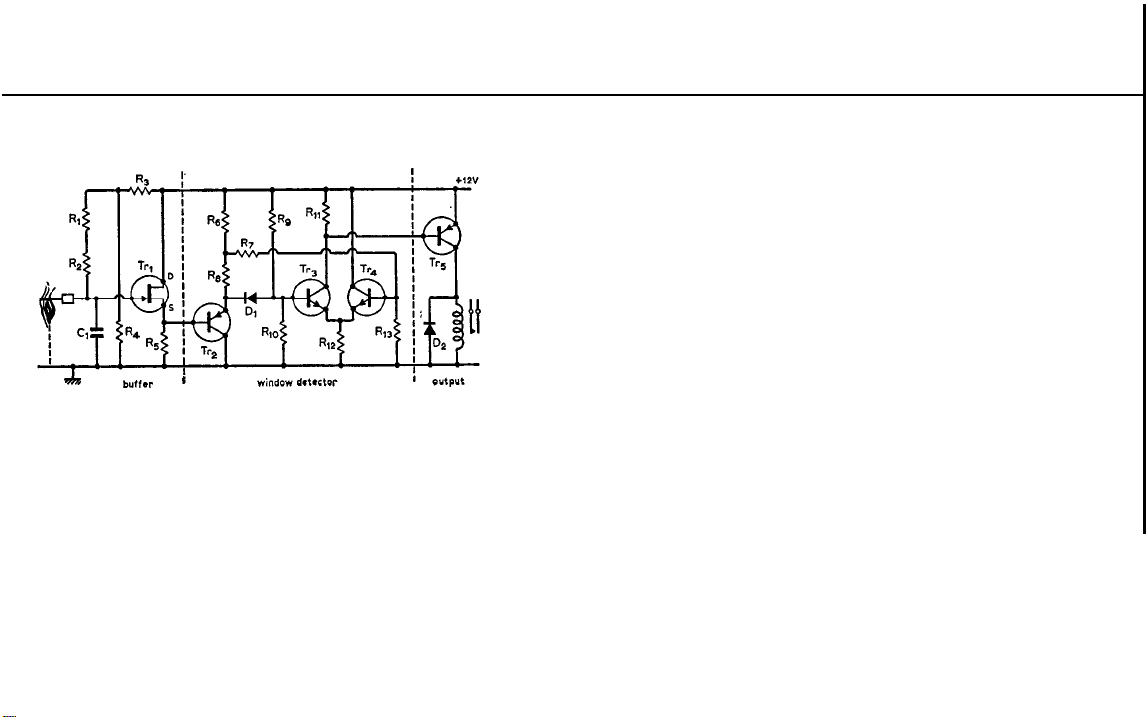
Flame detector
A flame offers a low conductance path to ground. In series
R1, R2,
with
the gate of Tr,, that leaves the emitter of Tr, at a high enough
potential to keep
bring Tr, into conduction via R,. Hence Tr,,
holding on the relay-interlocked with the supply for fail-safe
operation. If the flame is extinguished Trl gate goes high,
driving
Tr5
and the relay. A short circuit to ground at the input
reduces the base potential of Tr, bringing D1 into conduction
and cutting of
The mid-section of the circuit offers a window action with
the relay being held on for a restricted range of flame resistances, higher and lower values giving drop-out. The resistance
that conductance defines a range of potentials on
D1
Tr4
out of conduction, but not so high as to
on via
Trz, R7.
Tr3
and hence the output.
This removes the drive from Tr,,
Tr5
conduct
Component values
Tr,: TIS34
Tr,: BC126
Tr,: BC125
Tr,: BC125
Tr,: BC126
lN914
D,:
D,:
lN4002
C,:
1nF
R1,
R,:
15M
R,:
2.2k
_
R,:
12k
is high requiring a high input resistance buffer; the output is
conventional.
Smoke detector
When detecting the interruption of light by smoke, to
avoid the effects of ambient illumination etc., the light beam
may be chopped at source and the resulting a.c. from Tr1
(see over) used via buffer Tr, to trigger the monostable
Tr3,
circuit around
R10,
from rising sufficiently to fire the thyristor. If the load is
a horn having an interrupter switch in series with its coil, the
thyristor can cease conduction on removal of the gate drive
(alternatively a.c. drive to the load would be required).
Tr,. This prevents the potential applied to
R,:
6.8k
R,:
l.5k
R7
R9:
R8: 820R
R10:
Rll:
Rl2: 4.7k
Rl3:
Semiconductors not
critical but TIS34 may
need selection because of
parameter spread.
12k
15k
2.7k
22k
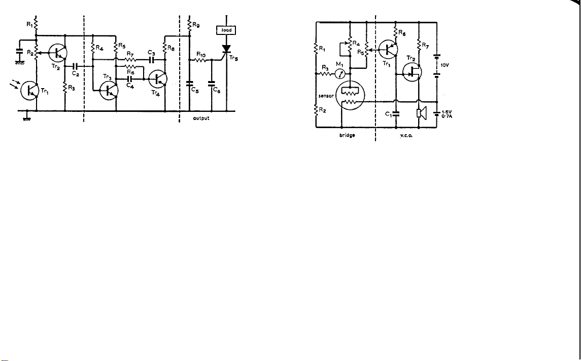
sensor
buffer ;
Tr1:
LS400
Tr2-4: 2N712
Tr5:
C106F
R1:
1k
R2, R8:
R3:
R4:
R5-7,
1OOk
15k
47Ok
R9:
1Ok
monostable
R10,
3.9k
C1,
16µF
C2,
C4: 22nF
C3: 0.lµF
C5:
50µF
C6: 4.7nF
Transistor types not
critical.
i
Gas detector
A particular gas-sensor (TGS from Figaro Engineering,
Shannon, Ireland) has two fine wires embedded in a
conductor. One is used to heat the material, with the
ance
between it and the second being reduced on the absorption
of deoxidizing gas or smoke. The sensor is sensitive to
<O.l %,
concentrations of
with resistance falling from many
tens of kilohms to as low as 1k at high gas concentrations.
Response is non-linear and with a recovery time in excess of
one minute. Bridge unbalance is detected on M1 and though
repeatable has to be interpreted qualitatively unless special
calibration procedures are available. When the unbalance
semi-
resist-
©
1974 IPC Business Press Ltd.
Tr,: BC126
Tr2:
TIS43
C1:
0.22µF
LS: 8 to 80 R
R1: 470K
R2:
3.3k
R3,
R5:
IOOk
R7:
lOk
1k
R4:
R6,
brings Tr, into conduction, C1 charges until the unijunction
Tr2
fires and the cycle recommences. The audible note in the
loudspeaker rises from a succession of clicks to a continuous
tone as the gas concentration increases. A Schmitt trigger
would allow relay drive, while the audible alarm could be
transferred to the flame-detector circuit, for example.
Further reading
Transducer detects gas, Electronic Components, 6 Nov. 1973,
p.18.
Wolfram, R., Fail-safe flame sensor provides control functions,
Electronics, 31 Aug. 1970, p.68.
Markus, J. (ed.), Smoke detector receiver, in Electronics
Circuits Manual, McGraw Hill, 1971, p.568.
Bollen,
D., Electronic nose, Practical Electronics, 1973,
pp.574-8.
Cross references
Series 2, cards 2, 3, 6
Series 9, cards 7, 10 & 11.
&
11. Series 8, cards 1, 3 & 8.
Wireless World Circard Series
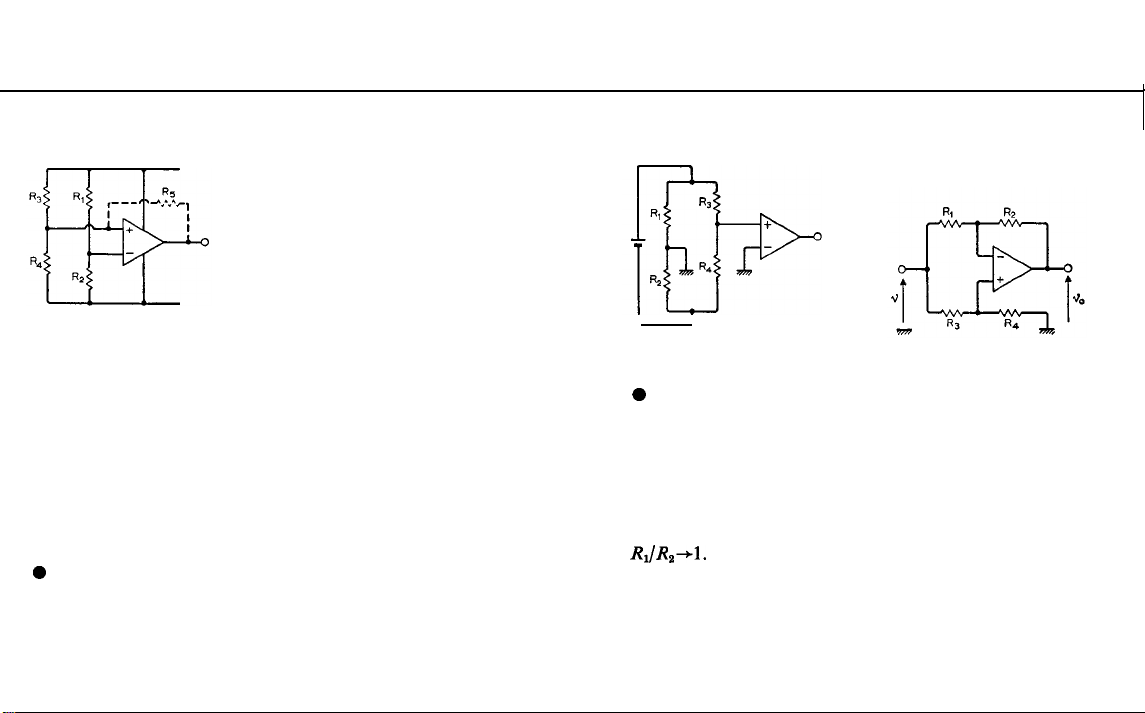
Bridge circuits
Components
ICs: 741, Vs
R1
to R4:
Bridge voltage:
Circuit description
Three bridge configurations are shown. In each case the bridge
is composed of four resistors, R1 to
basically Wheatstone bridges with balance occurring for
R1/R2=R3/R4. Substitution of impedances
leave the balance requirements unchanged, and other variants
such as the Wien bridge can be produced. For resistive
elements it may be possible to supply the bridge and amplifier
from a common d.c. supply and a high-gain op-amp detects
departure from balance. A small amount of positive feedback
R5
helps reduce jitter in the output when close to balance,
via
but gives hysteresis to the balance sensing.
*
If a separate supply is required for the bridge, one bridge
balance point may be grounded, removing the need for high
common-mode rejection for the amplifier. The errors in all
these circuits include voltage offset of the amplifier,
for untrimmed general-purpose op-amps, and input currents/
offset,
1OnA
to
1µA
for conditions as before. For balance
detection to within 0.1% this implies bridge voltages in excess
±15v
IOk,
R5:
1M
1.5V
(Fig. 2)
R4,
and the circuits are
Z1
to Z4 would
l-5mV
of 1V and currents of up to
0
By opening the bridge and embedding the amplifier in the
network as shown, balance is achieved for the same relationship between the resistances, but with input and output both
with respect to ground. This circuit has an output that is a
linear function of the departure of
condition
For d.c. applications the input may be one or other of the
supply voltages. In all cases best sensitivity is achieved for
R1/R+l.
have a low resistance, power wastage is avoided by keeping
the other pairs of resistances high.
l
Another method of achieving input and output as
referred signals, is to use an amplifier with push-pull outputs
and single-ended input. A simple case is the single transistor
as shown where the power supply, if properly by-passed,
closes the bridge when used for a.c. measurement/sensing.
13:
(R1, R3, R4
If the resistor whose value is being sensed has to
assumed constant as reference resistors).
Alarm Circuits-2
1mA.
R2
from the balance
ground-
-l-_. I
The example shown would pass all frequencies except the
notch frequency defined by l/RC, though with appreciable
attenuation near the notch.
0
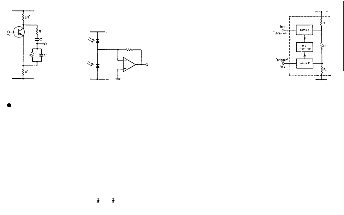
For many purposes, the availability of a centre-tapped
supply provides a “phantom-bridge” action. If the ratio of
positive to negative supplies remains constant then taking
one input of the sense amplifier to the centre-tap leaves only
I___-_-_---
voltage via a resistor chain with very good stability to the
ratio of their values; the absolute values are not important
for such an application. The lower-threshold detector
(“trigger”) when held high prevents any output change (input
1 is assumed high) regardless of the status of the reset terminal.
The reset terminal regains control only when the trigger input
falls below the level accurately defined by the potential
il.
---
a half-bridge externally. Used for example with photodiodes, divider. With the trigger taken from an external potential
the output voltage is proportional to the unbalance currents
in the diodes i.e. to the degree of unbalance in the illumination
divider containing the required sensing element the
balance sensing can be obtained.
bridge-
of the diodes. Because the diodes act as constant-current
devices the circuit is much more tolerant of drift in the
centre-tap than for purely resistive elements. The negative
feedback gives a linear output-unbalance characteristic. Manual, McGraw-Hill, 1971,
Reversal of the amplifier input terminals would give positive
feedback, introducing a switching action and hysteresis as
Further reading
Markus, J. (ed.), Bridge circuits, in Electronics Circuits
pp.84-9.
Graeme, Tobey
&
Huelsman, Operational Amplifiers,
McGraw-Hill, 1971.
in the first diagram.
l Some i.cs have internal potential dividers which can Cross references
effectively form part of a bridge. The 555 timer, for example, Series 1, cards 9 & 10, series 9, cards 1 & 11.
+
has its two comparators tapped at
and 8 of the supply
©
1974 IPC Business Press Ltd.
Series 13, cards 1 & 3.
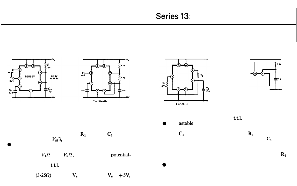
Wireless World Circard
Time delay and generator circuits
SeriesIs:
Alarm Circuits-3
Circuit description
An i.c. such as the 555, with internal comparators driving a
set-reset flip-flop offers great flexibility in the design of alarm
systems. With pin 2 high, the capacitor is held low via pin 7.
A negative-going edge on 2 allows
potential on 6 passes 2
0
Linking the inputs of the two comparators (2 and 6) to the
discharge path (7) causes the potential at the common point
to cycle between
divider. For both circuits the output has switching characteristics comparable to a
output stage. An audible alarm is available by connecting a
loudspeaker
the on/off condition of the alarm may be controlled by
(3-2552)
VJ3,
when the original state is restored.
VS/3
and 2
VS/3,
t.t.1.
gate because of a similar totem-pole
between Vs and pin 3. If V, is +5V,
R1
to charge Cz until the
set by an internal potential-
t.t.1.
driving pin 4 from the output of a
0
An
astable
output to the paralleled comparator inputs. When the output
is high,
threshold is passed; the output switches low and C1 is discharged until the trigger value set by pin 2 is passed. Timing
is set by the less well-defined output amplitude, and the
frequency is less stable than the basic circuit. Addition of
varies mark-space ratio.
0
If the reset terminal 4 is coupled to an RC network as
shown, then a time-delay can be introduced at switch-on,
before which firing of the circuit as a monostable can be
achieved.
can also be constructed by feedback from the
C1
is charged positively through R1 until the upper
gate.
Ra
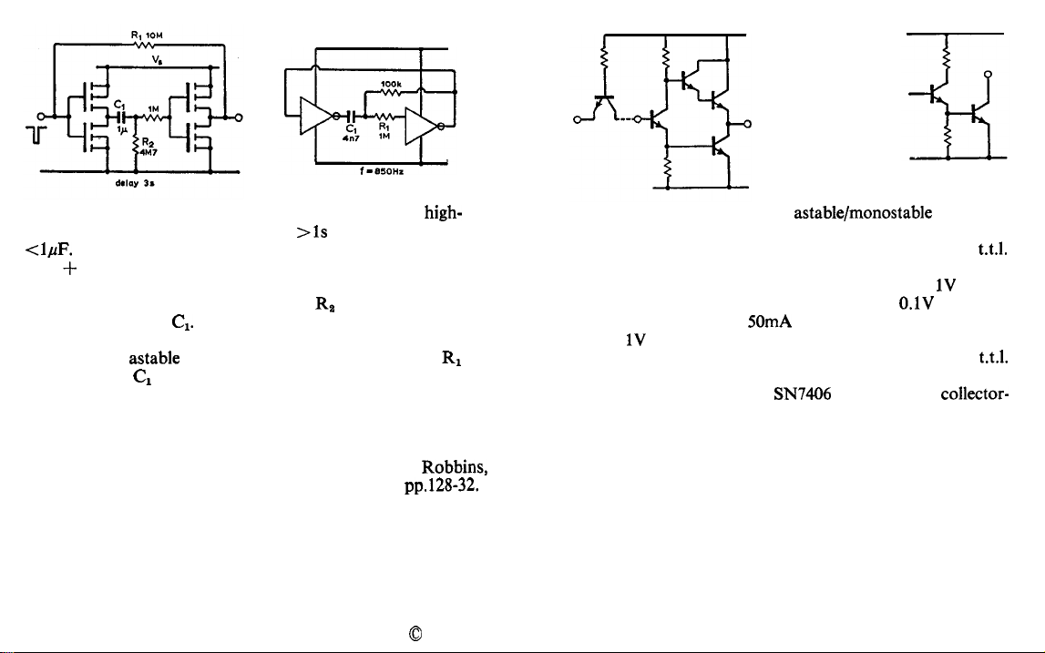
l A monostable using c.m.o.s. inverters can use very
value resistors, giving time delays of
<l,uF.
As shown, a short-duration excursion of the input
>Is
with capacitors of
high-
from + to ground sets the output to zero for the monostable
period (about 3s) because the output of the first inverter is
high, as is the input of the second until Ra can pull the gate
down by charging
C1.
The high impedance makes such
monostables useful as touch-operated circuits.
l
A related
astable
circuit shows an additional resistor
R1
which isolates C1 from the rapid charge/discharge imposed
by the gate protection diodes in both these circuits. The
resistor improves the timing stability.
Farther reading
Three articles, by
21 June, 1973,
Application note for XR-2556 timing circuit, Exar, 1973.
Cross
references
Series 3, card 9.
Series 13, card 5.
Robbins,
pp.128-32.
0
1974 IPC Business Press Ltd.
l The output stage of an astable/monostable circuit is
important where high voltage/current/power is required. For
the 555 timer, the output stage is similar to the typical
output (as shown above) but with a Darlington-connected
top section. The positive output is thus at least 1V below
supply while the low output can be to within
at low currents. Above
2V and 1V respectively.
l
For some applications the open-collector output of
devices such as SN7401 gives convenient driving of loads,
while other devices such as
emitter voltages of up to 30V.
Orrel and De Kold, in Electronics,
O.lV
50mA
the voltage drops may reach
SN7406
will withstand
t.t.1.
of ground
t.t.1.
collector-
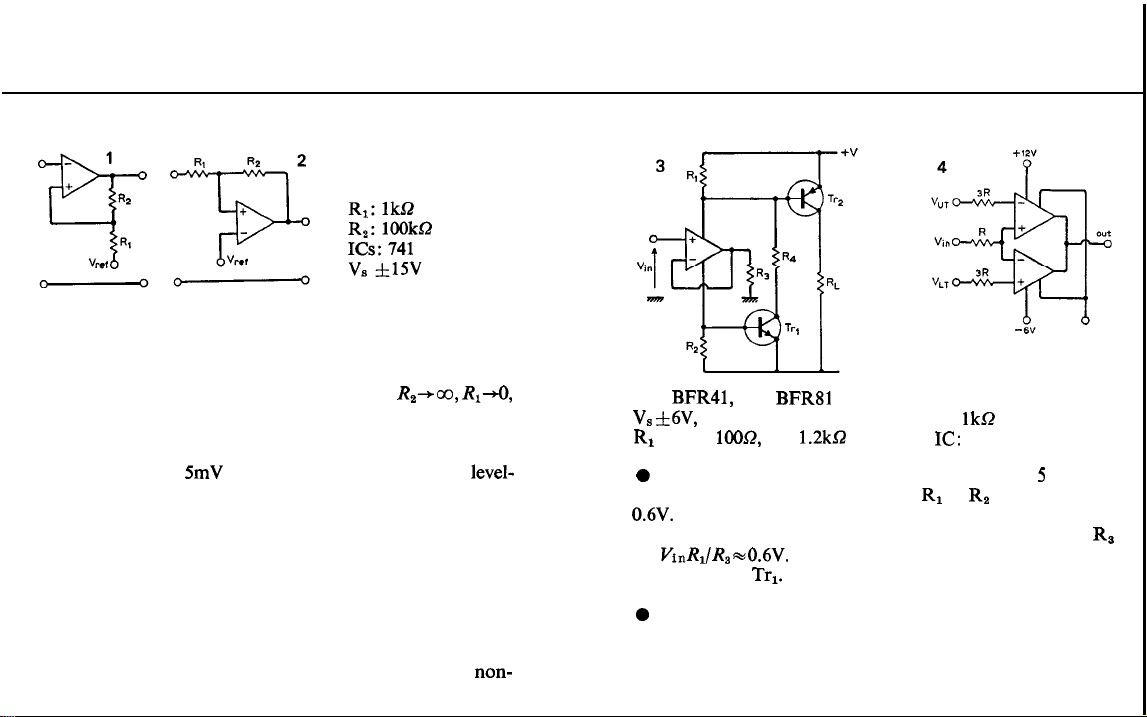
Wireless World Circard
Level sensing and load driving
Circuit description
The basic level-sensing circuits shown may be used with or
without positive feedback, to obtain an output change as the
input passes a defined level or levels. For
amplifier gain determines the range of input voltages for which
the output is not switched hard to one or other extreme.
(Typically 1 to 20mV for comparators, required to operate at
high speeds ; 0.1 to
sensing makes their slower operation an acceptable penalty.)
Hysteresis introduced by positive feedback allows the circuit
to latch into a final state after the first excursion through a
given level, provided the input cannot reverse its sense
sufficiently to pass back through the other switching level.
These circuits can thus perform the combined functions of
level-sensing and set-reset action required in many alarms if for
example the signal is a positive-going voltage initiating the
set action, while the reset action is a negative-going pulse
over-riding the former e.g. a resistor taken from the non-
inverting input to the negative rail.
5mV
for op-amps where accuracy of
R*-+~o, RI-d,
level-
Series 13:
Tr,:
BFR41,
Vs f6V,
R1
to R,:
0
An adaptation of the output stage shown in Fig. 5 gives an
output when the p.d. across either R1 or Rz exceeds about
0.6V.
voltage defining sufficient positive supply current via
i.e. VI~RJR,
the output via Trl. The switching action is not particularly
sharp as it uses only the gains of the transistors.
0
A standard window comparator gives sharper switching
but requires two amplifiers/comparators and still requires an
additional transistor is an output swing comparable to supply
voltage is required e.g. for efficient switching of lamps relays
etc., particularly at higher currents.
Tr,: BFRSl
RL: 20052
10052,
R,:
1.2kQ
In the former case this corresponds to a positive input
-0.6V.
Similarlyanegativeinput voltage switches
Alarm Circuits-4
R:
1kSL’
IC: 711
R,
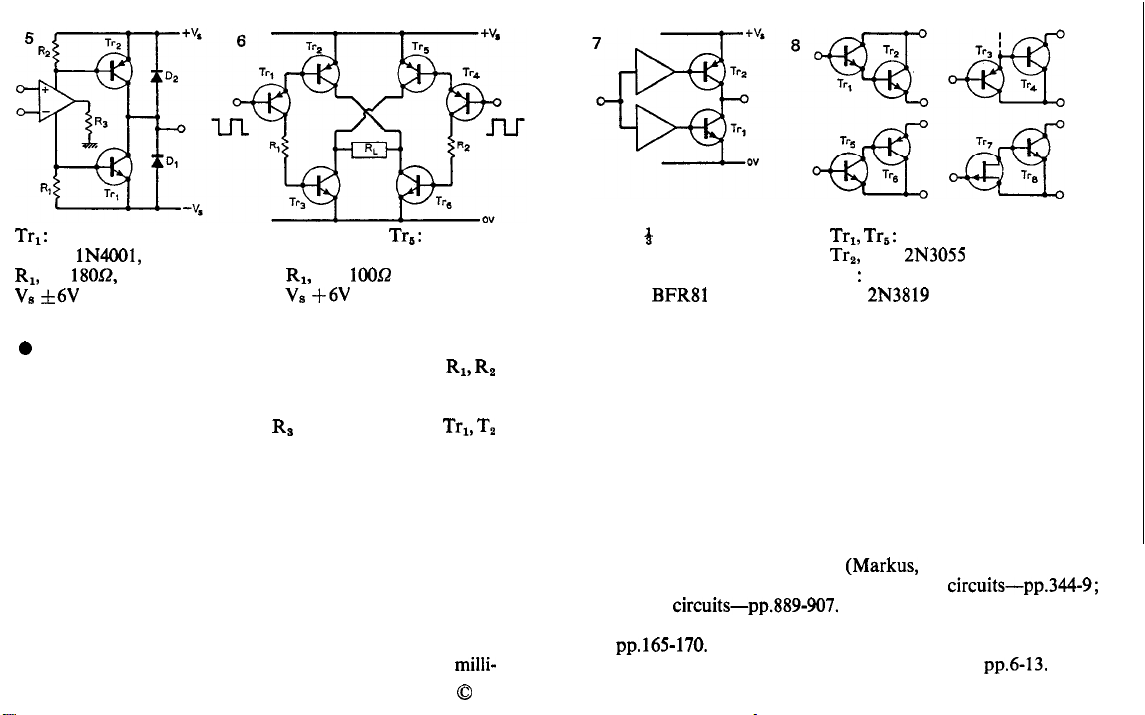
Trr: BFR41, Tr, BFR81
D,, D,:
Rr,
R,:
lN4001,
18OQ,
IC: 741
R,: 68052
Ve f6V
0
A previously-described output stage (series 2) gives
Tr,, Tr,, Tr,,
Tr,, Tr,: BFR41
R1,
R,:
Vs +6V
I
L up to 300mA
push-pull drive using one op-amp as driver. Resistors
1OOQ
Tr,:
BFR81
Rr, Rz
are selected to keep Tr,, Tr, out of conduction in quiescent
state. The op-amp is used in any of the sensing/oscillating
modes that result in p.ds across Rs sufficient to drive Trl, T,
into conduction. Either may be used alone for driving lamps,
relays, or the circuit as shown may be capacitively coupled
to a loudspeaker for a.c. power drive.
l
An output stage using a bridge configuration requires
antiphase switching at the inputs, but gives a load voltage
whose peak-peak value is twice the supply voltage. This is
equally applicable to audio alarms or to driving of servo
systems for which it was designed.
l Complementary m.o.s. buffers may be used to drive
complementary output transistors as shown and with the aid
of an additional inverter a similar stage provides a bridge
output. The transistor base current is limited to a few
milli-
0
1974 IPC Business Press Ltd.
IC: f CD4049
or CD4050
Tr,: BFR41
Trr, TrS:
Trz,
Tr, : MJE371
Tr,: BFR8l Tr,:
BFR41
Tr,:
2N3819
2N3055
amperes but in all these output stages, short-duration current
spikes may occur during the output transitions. Diode
protection against inductive voltage spikes as in Fig. 5
should be used for loudspeaker, relay and solenoid loads.
l
Any of the output transistors may in principle be replaced
by the compound transistor pairs if higher peak currents are
needed. To reduce the above requirements it is worth
considering the use of f.e.t. devices as the input transistor
of the pair.
Further reading
Electronic Circuits Manual (Markus, McGraw-Hill 1971):
Main circuits-pp.l-6; lamp control circuits-pp.344-9;
trigger
circuits-pp.889~907.
Linear Integrated Circuits Handbook, Marconi-Elliot,
pp.165-170.
Industrial Circuits Handbook, SGS-Fairchild,
pp.6-13.
Wireless World Circard Series 13:
I
Applications of 555 timer
Alarm Circuits-5
Circuit description
The 555, designed as a timing circuit with either monostable
or
astable
it to be used for many other purposes. In alarm systems, the
power output stage that permits currents of either polarity
of up to 200mA (though 50mA minimizes voltage losses)
means that lamps and relays can be driven quite readily.
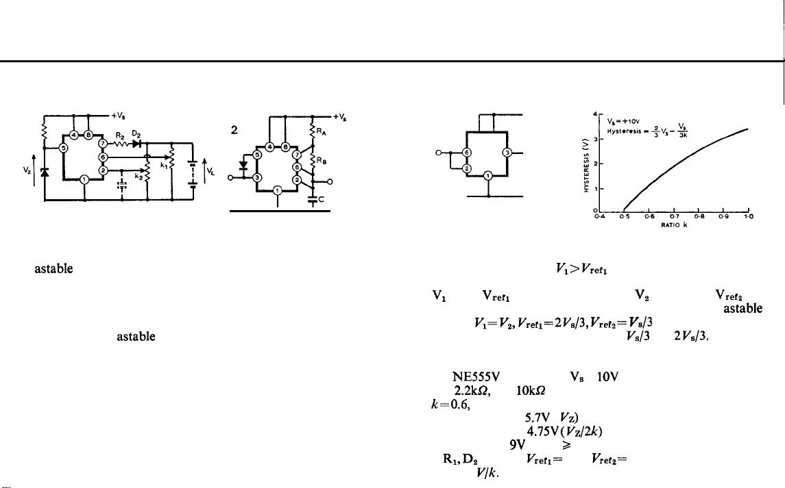
When used as an
be applied to a loudspeaker to give an audible alarm, while a
voltage fed to the control terminal modulates the frequency
for warble or two-tone effects. As a monostable circuit it can
be used to provide delays from microseconds to minutes,
allowing, for example, a warning alarm to be held for a
defined period of time after the appearance of the condition
being detected. In such cases the condition (closure of a
switch in a burglar alarm for example) is converted into a
negative-going pulse, applied to the trigger input. A further
application for the device involves the controlled hysteresis
operation, has internal circuit functions that allow
astable
circuit the output square wave can
provided by the two comparators biased from an internal
potential divider. With
via the flip-flop which ignores any further excursions of
V,
about
Vrerl
flip-flop is reset, the output going positive. In the astable
circuit
is charged and discharged between
in either sense. When Va falls below
VI=
V,, V,,r,=2Vs/3,
VI> V,,f,
V,,r,=
the output is driven negative
Vrerz
the
Vs/3
and the capacitor
Vs/3
and
2Vs/3.
Typical performance
IC:
NE555V
R,:
2.2kQ,
k=0.6,
Upper set point:
Lower set point:
Output swing: 9V for
If
R1, Dz
2V and V/k.
(Signetics), Vs +
R,:
D,: 5.6-V Zener diode
1OkD
5.7V
(
4.75V
RL >
omitted, VM,= 2 V, Vrer,= V and set points become
VZ)
(Vz/2k)
25052
1OV

Component changes
IC:
Vs:
RI, D,:
R,:
Motorola
used with independent reference voltages or a single
comparator with hysteresis defined by
see Series 2.
4.5 to 18V. At low voltages the saturation voltages
at the output may not allow adequate drive to
electromechanical/filament lamp loads.
Any network to provide constant voltage at control
input. Voltage may be to within 1V of common line
or positive supply, but for optimum performance
should be close to
lk to
source; at high values inaccuracies due to threshold
current of up to
MC1455
Separate comparators could be
2Vs/3.
1MQ.
At low values, excessive loading of
0.25,uA.
Circuit modifications
l
Use as battery charger illustrates method well (above).
Upper threshold when ~,VL=
k,VL= Vz/2.
When upper threshold is exceeded output at
V,;
lower threshold when
feedback-
0
1974 IPC Business Press Ltd.
pin 3 reverse-biases diode Dz and battery discharges into load
when present. As voltage VL falls below lower threshold,
voltage at pin 3 rises and charges battery through limiting
resistor
Vzlk,+ V&k,.
l To increase hysteresis, the potential at pin
Rz.
Hysteresis may be reduced towards zero for
5
may be
reduced following a transition through the upper threshold.
This may be done as in Fig. 2 by using output pin 3 via a
diode-both thresholds are varied if the diode is replaced
by a resistor.
l
The increased swing similifies the triggering of a following
555 used as a Schmitt trigger, as the capacitor voltage in
Fig. 2 can approach zero. Complete alarm systems can be
based on such circuits combining level sensing, time delays
and waveform generation, as well as audible alarms.
Further reading
Four articles, by De Kold, McGowan, Harvey & Pate, in
Electronics, 21
June 1973,
pp.128-32.

Wireless World Circard Series
Frequency sensing alarm
at a lower frequency (f/20), and hold on during signal failure
or for temporary interruptions of the signal.
The upper frequency in the band mode or the datum in the
datum mode is set by
tl+ tr.
to comparators Schmitt-triggers and window-comparators.
Typical performance
IC: FXlOl (Consumer Microcircuits) [OBSOLETE PART]
Circuit description
The circuit is a monolithic m.o.s. i.c. which uses external
RC elements to fix the frequencies at which the circuit
orovides
switching times defin;d by
monostable circuits with the second time interval being
initiated at the end of the first. The input may be a repetitive
signal of arbitrary waveform, provided the amplitude is in
excess of
pk-pk). Internally this is presumably squared by a Schmitt
type of circuit to trigger the monostables. Three distinct
conditions may exist; if the period of the received signal is
t=l/f
t<tl, tl<t<tl+tz, t>tl+tz.
guished by additional internal circuitry that allows sensing of
frequencies above a given datum or within a given band with
a switched output that can be made to latch on or off, toggle
a switching action. If does so via two senarate
1OOmV
pk-pk (though it should not exceed 20V
and the two delays are
CIR,
and
CaRa,
as from a pair of
t,=k/C,R, t,=kjC,R,,
These conditions are distin-
then
vi*:
R1,
R,:
c,:
Ground pins: 2, 3, 9.
Gutout on for:
Pin
i
2
3
5
9
13:
The circuit provides frequency-sensing function similar
-
12V supply,
250mV pk-pk to pin 1
47OkQ
22nF, C,: lOnF,
f>lSOHz (f% 1/0.6C,R,).
signal input.
grounded, holds switch state during signal loss.
open, switch off.
ground via ‘c’, switch off after signal break of
for
‘c’.
ground, circuit automatically resets on change off.
open, switch latches when turned off.
link to 8, switch latches when turned on. Ground 3.
link to 8 via ‘C’, hysteresis in datum point of
100%.
ground, datum mode, switches on for
open, band mode, on for
link to pin 5, output toggles at f/20 when in band.
Alarm Circuits-6
t1
and the lower band-frequency by
-3mA+
C,:
load current
O.l.uF
fi>f >fi.
f
2OOms/pF
‘C’/C,x
>fi.

EI
0”
R
-4
to
to
to
(b)
to
1MB
1pF
SOkHz.
1pF
(not critical)
C,= C,=
(&+Rn+Rc)C
C, variation
i.e. it is the
0
1974 IPC Business Press Ltd.
(a)
-=
Component changes
Vs:
-12 to -22V some samples operate with reduced
Vin:
0.1 to 20V pk-pk
freq. set points:
response time :within 5 to 10 cycles of receipt of correct
Circuit modifications
l
As the lower frequency in the band mode is affected by
time constant
frequency is not, variation of R, increases the band by
variation of its lower bound only. For
in the tapping point of RC in (a) at left leaves the sum of the
time constants unchanged at
lower frequency that remains constant while the upper
frequency is charged.
accuracy down to -8V.
O.OlHz
frequency.
1OOk
250pF
1OnF
CaRa
in the original circuit while the upper
0
t
kc
I
Y
l
Variation in both frequencies while retaining a reasonably
constant ratio of
be achieved by varying the common bias applied to the
resistors. If strong dependence on supply voltage is to be
avoided the bias voltage should be supply-proportional as
in (b).
l
Constant-current sources allow linear control of period
against a separate reference voltage, which may be
proportional.
l
Filament lamps may be driven via an additional transistor, currents up to
on right. Direct drive of reed relays, l.e.ds is possible though
current is marginal.
Further reading
Volk, A. M. Two i.c. digital filter varies
Electronics,
McKinley, R. J., Versatile digital circuit filters highs, lows
or bands.
FXlOl : Consumer Microcircuits data sheet D/026.
Cross references
Series 1, cards 6 & 7.
Electronics, 21
8
fi:fi
(the equivalent of a constant
lOOmA
15 Feb. 1973,
June 1971, p.66.
Q),
supply-
or so being provided by circuit
passband
p.106.
easily,
can

Wireless World Circard
Digital alarm annunciators
ICs:
1-3, 5, 7-15
)
x
SN7400
#x
SN7410
4,6,
r: 3.3k52,
Circuit function
It is assumed that a fault condition is the opening of relay
contact RLr, though any other sensor that maintains the
NAND-gate input terminal at a low
A fault will turn off a “safe” green light and illuminate a
“danger” red light, and operate an audible alarm. When the
“recognise” push-button is depressed, the red light stays on,
but the alarm is silenced. When the fault clears, the alarm is
restarted, the green light comes on and the red light goes off.
(‘0’)
level is adequate.
R,:
68Q
Series 13:
The “recognise” button is again pushed to reset circuit to its
normal state.
Alarm Circuits-7
Circuit operation
Consider the circuit in its normal state where inputs R, T and
F are at zero volts (or binary zero) i.e. R=T=F=O. This
makes
X=0(x= l),
(green) and
If a fault occurs,
i.e.
F=l,
remains as before. Hence
Pushing the
T=O, then
remains on, but A=O, and alarm stops. This state will be
maintained until the fault is cleared.
but
A= 1, and the alarm operates,
R=l,
R=l,
alarm, when started from normal state with LED, on.
causing
When the fault is cleared, R=F=T=O, Y does not change,
X=0 (Y=z=l, X=p=O).
Final recognition of the fault clearance is obtained from
which will return circuit to its normal state i.e. for
F=T=O, Y=O and
Depression of the test button will check
Circuit modification
As X, R, Y, p are available, the
elusive-OR function of A can be obtained as shown.
Y=O
LED2
(red) is off.
RLt
X=0 (;iz=l),
recognise
Y=l @=O>,
(P=
1) and hence
opens, F goes high (or binary one)
but the state of Y (and
A=l,
and triggers audible alarm.
button causes R= 1, and as F= 1,
but X does not change. LED,
Hence
X=0.
ex-
LED1
LEDz
X
F
2
Y
is energised
is illuminated,
LED1
and the
P)

;
1
+v
Circuit description
Complementary-m.o.s. devices may be. used in the circuit
above to minimize stand-by power consumption.
Normal safe condition obtains with
the fault-switch closes,
X+0.
Hence L=O, E= 1, opening gate
F-t1
L=A=O, F=
1. When
and since L is already high,
ICr,.
Also since F=O,
Y+O, and hence A is forced to zero, therefore A= 1. This
transition may be used to switch an audible alarm. Simultaneously the oscillator gate is opened which will cause lamp
flashing at a rate determined by the astable frequency.
If the fault is rectified, the alarm condition is maintained
until the clear button is pressed causing C to be low. Hence
L-+1,
and will latch in this condition via memory circuit
and
ICI.
Also E=O, thus
tained via ICI and
x=0,
this condition being main-
IC5,
and the alarm is silenced.
IC2
Circuit description
Arrangement right allows detection of first-fault occurrence
from three sensors
the number of inputs available per NAND-gate.
Sr, Se, Ss,
this number being restricted by
0
1974 IPC Business Press Ltd.
i
+V,(+SV)
Outputs
Qa, Qs, QB
are set to zero when the reset button is
depressed. The 0 output of each flip-flop is applied to the
other two NAND gates, but not to the one associated with
itself. Hence two of the three inputs of each gate are high.
If S, closes, for example,
IC2
output goes low, and this
negative-going edge being applied to IC, preset terminal sets
Q&=1
(and hence
q=O).
Therefore ICI and
ICs
are now
inhibited and cannot respond to a fault condition.
Further reading
Zissos, D., Logic design algorithms, Oxford 1972.

Wireless World Circard
Filament lamps and relays
Filament lamps are widely used as visual alarm indicators
and often connected in the collector-emitter circuit of a
bipolar transistor that is switched on and saturated under
alarm conditions. These lamps have a positive temperature
coefficient of resistance with a large difference of resistance
between the cold and hot states-see Graph 1 which is typical
for a 6-V,
voltage source, a large current surge flows in the lamp, and
switching transistor, which then decays exponentially to its
normal or rated value in the hot state. This surge may be
ten times the rated current, or even higher, shortens the life
of the lamp, may destroy the switching transistor or blow the
power supply fuse. Graph 2 shows the typical initial surge
current characteristic of a 6-V,
thermal time constant of about 2ms.
lO@mA
panel lamp. When switched on across a
60-mA
panel lamp having a
Series 13:
When lamps are used as flashing alarms, the initial surge
current is as shown in Graph 2 but the surge current on
successive pulses depends on the thermal time constant and
the time between flashes. Graph 3 shows the typical variation
in surge current when a 6-V,
on for 5 s then off for t
If the p.d. applied to the lamp is gradually increased the
current rises in a controlled manner to its normal operating
value, prolonging the life of the lamp and reducing the
probability of transistor damage. A simple arrangement is
shown above where Tr, is normally held on and saturated
with a low value of
Under alarm conditions, the base drive to Tr, is removed
and the capacitor charges through Rn. The base voltage of
Trl rises exponentially so that the lamp surge current is
avoided.
Vc~(sat)
Alarm Circuits-8
60-mA
panel lamp is switched
,,rr
seconds.
holding Tr, and the lamp off.

To prevent damage to
circuited, a resistor Rc could be included in
Trr
should the lamp become short-
Tr,‘s
free collector,
but this would reduce the lamp voltage in normal operation.
Circuit above shows a modification that ‘allows an almost
normal lamp voltage and also limits the short-circuit current
to the desired value by using only a small Rc value and a
saturating transistor Tr,.
Relays are used to actuate alarm devices that need to be
isolated from their control circuitry for various reasons such
as their current, voltage or power requirements being incompatible with the electronic circuitry. Circuit right,
acommonly-
used relay drive circuit which takes into account both the
resistive and inductive properties of the relay coil. When
actuated, the steady-state coil current is fixed by the coil
resistance and supply voltage, but when Tr, is turned off the
inductance of the coil causes the collector voltage to rise
towards a level greatly exceeding V CC if the protective diode
D,
were omitted. Diode D1 allows
VCE
to rise only slightly
above Vce before the diode conducts to dissipate the energy
stored in the relay coil. When Tr, turns on D1 is
reverse-
biased and does not affect the operation. The diode must be
able to withstand a reverse voltage slightly greater than V CC
0
1974
IPC
and be able to conduct the relay-coil discharge current for a
brief time. Transistor Tr, must have a V CE rating exceeding
Vcc and be capable of carrying the relay operating current.
If a relay is required to operate when an input level exceeds
a certain predetermined value, it may be included in a Schmitt
trigger circuit; e.g. the relay coil and protective diode could
replace R1 in the basic circuit of series 2, card 2.
If the alarm indication uses a
1.e.d.
or alpha-numeric array
of l.e.ds consult series 9, cards 2, 5 & 6.
Further
reading
Shea, R. F. (Ed), Amplifier Handbook, section 3 106, McGraw-
Hill 1966.
Egan, F. (Ed), 400 ideas for design, vol. 2,
pp.18/9,
Hayden,
1971.
Cleary, J. F. (Ed), Transistor Manual,
pp.202,
General
Electric Co. of New York, 1964.
Industrial Circuit Handbook, section 2, SGS-Fairchild, 1967.
Cross references
Series 2, card 2.
Series 9, cards 2, 5 & 6.
Series 13, cards 4 & 7.
Press Ltd.

Wireless World Circard Series
Signal domain conversion
Fig.
Fig. 1
2
Fig. 3
A
13:
Fig. 4
Alarm Circuits-9
R2
Voltage-to-current conversion
It is often required to supply signals to relatively long transmission lines in which case the signal is more convenient in
current form rather than as a voltage. Thus,
current converters are useful and may be realized using
operational amplifiers especially if the load is floating.
Figs. 1 & 2 show the more common forms the former being
an inverting type and the latter non-inverting. In both Figs.
i=
Vin/R
and is independent of the load impedance, but the
source and operational amplifier must be able to supply this
load current in Fig. 1, whereas little source current is needed
in Fig. 2 due to the high input impedance of the amplifier.
Fig. 3 shows another floating-load V-to-I converter which
requires little source current if R1 is large and allows iL to be
scaled with R,, the operational amplifier supplying the whole
of the load current;
iL=
Vin(l/R, +
RP/R1R3).
of Fig. 4 is suitable for V-to-I conversion when the load is
voltage-to-
The circuit
grounded. When
R, and the current source impedance seen by the load very
R1R3= R,R,
the load current is
iL= -
Vi,,/
high.
Current-to-voltage conversion
If a device is best operated when fed from a voltage source
but the available signal is in the form of a current, a current-
to-voltage converter will be required, one example being shown
in Fig. 5. Current is fed to the summing junction of the
operational amplifier which is a virtual earth so that current
source sees an almost-zero load impedance. Input current
flows through R1 producing an output voltage of Vout=
volts/amp. The only conversion error is due to the bias
current of the operational amplifier which is algebraically
summed with
iin.
The output impedance is very low due to
the use of almost 100% feedback.
-
RI

Cl
I
Fig. 6
Fig.
1
I
Voltage-to-frequency conversion
Many voltage-to-frequency converters exist, the circuit
complexity often being a guide to the degree of linearity and
maximum operating frequency. Fig. 6 shows one form of
V-to-f converter (a
below about
differencing
LM3900
v.c.o.)
suitable for use at frequencies
lOkHz,
each amplifier being of the current-
type. Amplifier A, is connected as an
integrator with AZ acting as a Schmitt trigger which senses
the output from AI and controls the state of Tr, which either
shunts the input current through Rz to ground, making
Voutl
run down linearly, or allows it to enter AI causing
Voutl
to rise linearly with
wave and
Vout,
a square wave having a frequency that is
linearly dependent on
RI=
2R,.
So
Voutl
is a triangular
RI, C1
and the threshold levels selected
for the Schmitt trigger.
Frequency-to-voltage conversion
Diode-pump, transistor-pump and op-amp pump circuits
are widely used for low-cost frequency to voltage conversion.
Another circuit, using a single
LM3900
quad currentdifferencing amplifier package, is the phase-locked loop
shown in Fig. 7 which uses the
is in the
LM3900
package used as a phase comparator having
V.C.O.
of Fig. 6. Amplifier A,
a pulse-width modulated output depending on the phase
difference between
Vin
and
VOUtg
of the
V.C.O.
Resistor
R8
and C, form a simple low-pass filter which makes the d.c.
output vary in the range +V to
+V/2
as the phase difference
changes from 180” to 0”. This direct voltage controls the
frequency of the
V.C.O.
and its lock range may be increased
by using the fourth amplifier in the package as a d.c. amplifier
between the filter and the integrator. Centre-frequency of the
p.l.1.
is about 3kHz with:
30kQ; R5, RB 1.2MQ; R, 62kSZ;
RI, R,
C, 1nF; C,
1MR; Rz
510kSZ;
1OOnF;
R,,
R8, Rg,
V= $4
to +36V.
Further reading
Graeme, J. G. & Tobey, G. E. Operational Amplifiers,
chapter 6, McGraw-Hill 1971.
Linear Applications-Application notes AN20 and AN72,
National Semiconductor 1973.
Cross references
Series
3, cards 3,5 & 10.
Series
13. cards 1& 6.
0
1974 IPC Business Press Ltd.
Wireless World Circard Series
Pressure, temperature and moisture-sensitive alarms
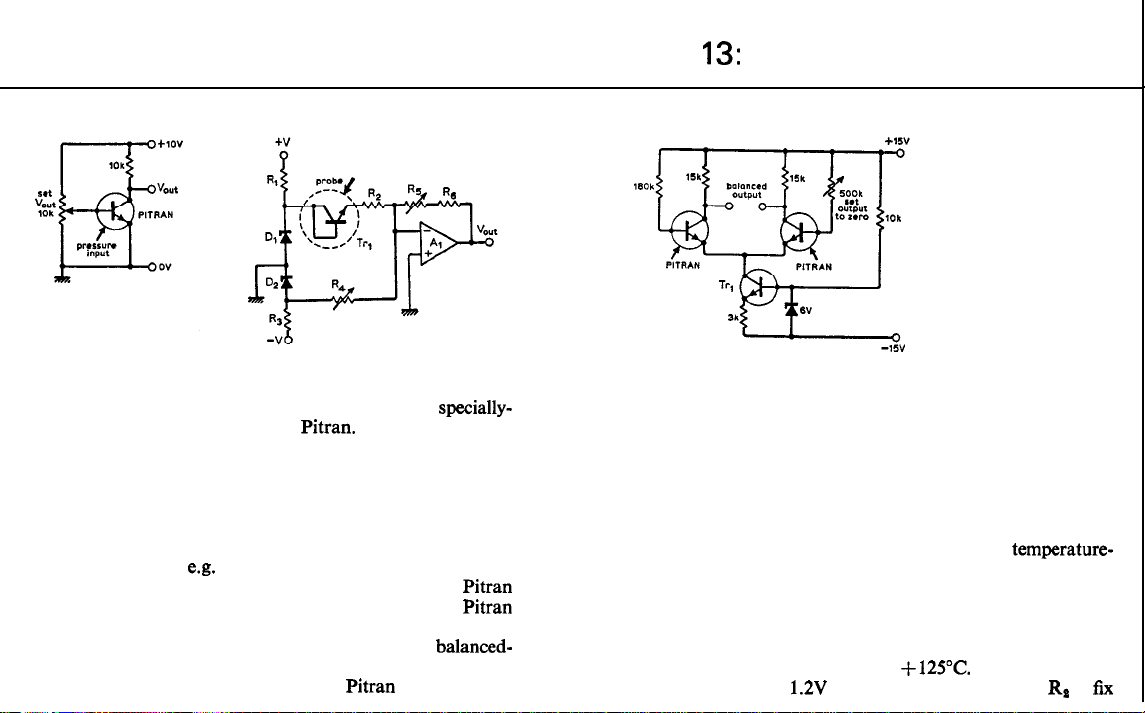
Pressure-sensitive alarm
A pressure-sensitive alarm may be made using a
modified transistor known as the Pitran. It is a planar n-p-n
transistor having a diaphragm mounted in the top of its metal
can which is mechanically coupled to its base-emitter junction.
When a pressure is applied to the diaphragm a reversible
charge is produced in the transistor characteristics. The
mechanical pressure input can be used to directly modulate
the electrical output of the transistor which may be fed to
the alarm circuitry
which switches state when the input pressure to the Pitran
either exceeds or falls below some critical level. The Pitran
may be connected as a single-ended-input single-ended-output
stage, as shown left or as a differential-input
output stage, as shown middle. Conventional transistor circuit
design techniques may be used for the Pitran stages. Linear
e.g.
via a comparator or Schmitt trigger
specially-
balanced-
output voltages of up to one-fifth of the total supply voltage
are obtainable.
Temperature-sensitive alarm
Circuit above shows the input circuitry of an alarm which may
be operated by the output signal from the operational
amplifier when the temperature monitored by the probe
transistor exceeds a pre-determined value. The temperature-
sensing transistor is a low-cost n-p-n type that can produce
a resolution of less than 1 deg C in a temperature range of
100 deg C. If the operating current of the probe transistor is
made proportional to temperature, the non-linearity of its
base-emitter voltage may be minimized, being less than 2mV
in the temperature range -55 to +125”C. Zener diodes set
the input voltage to
13:
Alarm Circuits-10
1.2V
and this is applied through RI to
fix

the operating current of the probe transistor. Resistor
R4
may be adjusted to make amplifier’s output zero at 0°C and
R&
is used to calibrate the output voltage to
lOOmV/deg
C,
or any other scaling factor, independently of the Vout= 0
condition. RI, Rs
D1, Da
LM113; TrI
12ksE; Ra 3kQ; R, 5kSZ; Rs, RB 1OOkQ;
2N2222;
Al LM112; V
hl5V.
Moisture-sensitive alarm
A low-cost audible alarm which operates when the electrodes
of the input sensor become damp due to increase in humidity,
direct contact with water, rain or snow is shown above.
The sensor is conveniently made from parallel-strip printed
circuit board or commercial equivalent, so that increase in
moisture at the strips produces a very small current to Trl
base via RI which forms a high-gain compound pair with Tr,
which switches hard on. Transistors
Trs
and Tr, form the
0
1974 IPC Business Press Ltd.
audible alarm multivibrator, that acts as a load on the
compound pair, having a repetition rate determined by the
C,R, time constant. A piercing note at about 2SkHz is
produced with RI, R,
ZTX300; Trs
OC71; LS 8-Q loudspeaker; V +9V.
lOOkS2; RJ lkS2; C1 1OnF;
Tr,, Tr, Tr,
A flashing display with a rate of about 2Hz may be obtained
by replacing the loudspeaker with a 6-V,
and changing the values of Rz to
470kQ
60-mA
panel lamp
and C1 to
2.2pF.
Further reading
Tingay, E. The Pitran-a new concept in pressure measure-
ment,
International Marketing News, p.8,
Linear Applications-application notes AN3 1, AN56 and
AN72, National Semiconductor, 1973.
Brown, F. Rain warning alarm, Everyday Electronics,
pp.208-11,
1972.
1970.

Wireless World Circard
Security, water level and automobile alarms
I
Vl
-I
--
Circuit description
Component R, is the resistance in the search loop which if
obtained using two
switches either in series with the loop or in parallel with either
resistor, or both. In the latter case changing a switch condition
from open to closed in the parallel case and from closed to
open in the series case can give rise to either a positive voltage
or a negative voltage being applied to the diode bridge; the
bridge is, of course, balanced initially. The diode bridge
being a full wave rectifier will apply a negative
following circuit in either case.
The bridge resistors are large valued to minimize current
drain from the battery but requires that the following circuit
have a large input resistance. Hence the Darlington pair Tr,
and
Trz
is employed.
When vbs goes negative, Trl and with it Tr,, conducts.
Transistor
TrB
lOOkS2
resistors allows one to include
then drives Tr, which is a higher power device
+
Y
Vba
to the
Series 13:
capable of drawing a relay coil to produce the warning
signal. At the same time when
TrS
goes negative and hence via positive feedback through
the base of
zero. Hence, a latching action is obtained, which keeps the
warning signal on. The warning signal will only be removed
if the power supply is removed.
Capacitors C1 and Ca are required to prevent spurious
pulses from triggering the alarm, in the case of
prevent switching transients from triggering the alarm when
the alarm is being reset, in the case of
Tra
remains negative, even if
Alarm Circuits-II
Trs
conducts, the collector of
Vba
is set back to
C1,
and to
Ct.
Component values
Tr,,
Trz:
R1, R,: 15OkQ
R,:
2OOkB
R,:
25OkQ
variable
R,:
27kQ
R,: 47052
Ci,
C!,: 0.33/tF
Tr,: BFR41 or BFY52
Diodes 0A81
V,:
vs: 9v
BC126
18V
Brake light monitor (circuit over)
Both of the identical counter-wound coils are wound round
the reed relay. Hence the relay switch will only close, giving
a dashboard warning, if either of the brake lights fails either
with an open circuit or short circuit.
Rs
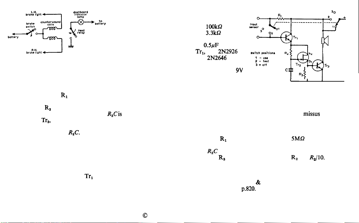
Water level alarm
This circuit is designed to produce a note from the loudspeaker when the sensor input terminals are shorted. As such
it can be used for many applications apart from suggested
water level/rain alarm. When the input terminals are shorted
base drive to Tr, via R1 is obtained, and the supply voltage
is switched to the unijunction relaxation oscillator comprising Tr,, R,, R, and C (card 4, series 3). A train of pulses of
period mainly determined by the product
to the base of
the loudspeaker. The loudspeaker alarm note can be altered
by altering the product
can be obtained by selecting the note to correspond to the
resonant frequency of speaker. In practice the alarm will
sound for any resistance between zero and five megohms.
The quiescent current of the unit is of the order ofnanoamps
so that battery life is many months even if the unit is switched
off. Provision to test the battery condition is made by switch
position 2 which should cause Trl to switch on the oscillator
provided the battery is in good condition.
For water level sensing two conducting rods spaced an
inch, or less, apart and positioned at the required level is all
that is required.
Tr,,
thereby producing pulses of current through
R&T.
Considerable effective output
R&is
then presented
Component values
R,:
lOOks2
R,:
3.3kQ
R,: 27052
C:
0.5,uF
Trl, Tr,:
Tr,:
LS: 8-Q loudspeaker
Supply voltage:
paper will suffice. When the blotting paper becomes wet
contact between the rods is made, the alarm sounds and the
washing is saved once more (provided the
shopping).
2N2926
2N2646
For a rain alarm two rods separated by some blotting
(G)
9V
‘Wit& po,i,l0”,
1 -Us.
P - tslt
3 - ott
‘f Ra( “(
missus
isn’t away
Component changes
Resistor R1 may be any value up to
shorting of the sensor input terminals is obtainable.
The R,C product is dictated by the pitch of the note required.
Resistor Rs should be much less than R, e.g.
5M.Q
provided a true
R&O.
Further reading
Andrews, J. Security Alarm,
Moorshead, H. Rain & Water Level Alarm, Practical
Electronics,
Morum, S. W. F., Brake Light Monitor, Practical Electronics
1973, p.588.
1971,
p.820.
Practical Electronics,
1973, p.338.
0
1974 IPC Business Press Ltd.
Wireless World Circard Series
Electromechanical alarms
Electromechanical transducers are obtainable in a wide
variety of types: they may be d.c. or
or capacitive, contacting or non-contacting, analogue or
digital, linear or angular, etc. Insofar as most alarm systems
use a comparator (cross ref. 1) to compare the signal with a
reference and as d.c. signals are easily compared we shall
assume here that any a.c. systems are followed by signal
conditioning equipment which includes a rectifier (cross ref. 2)
of some sort so that the effective output is d.c.
a.c.,
resistive, reluctive
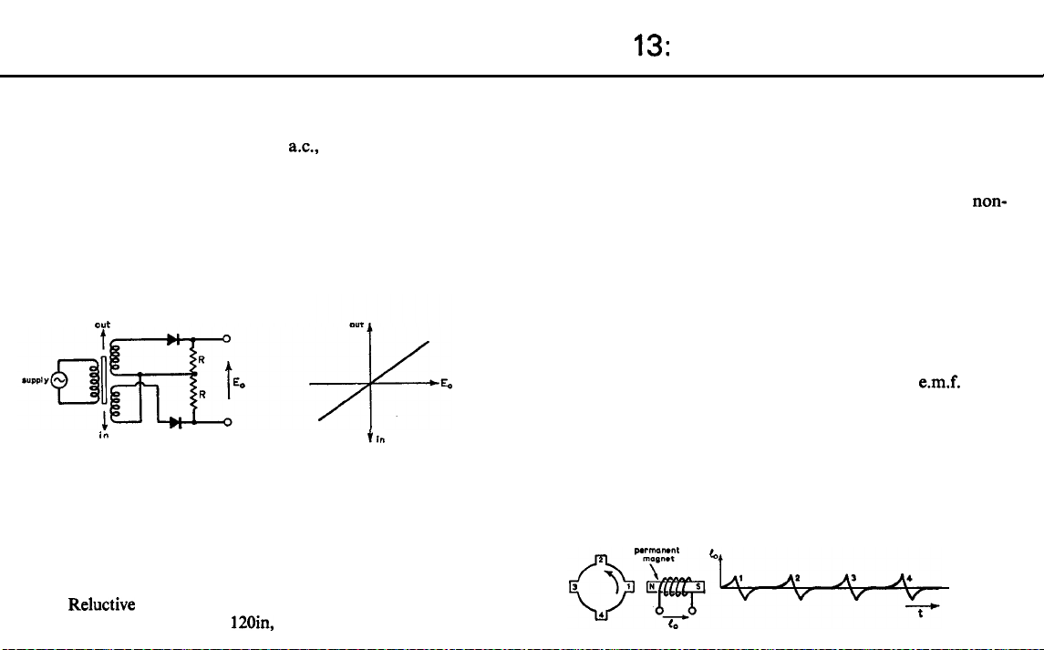
Displacement alarm
O”t
in
Circuit shows a reluctive displacement transducer, of the
differential transformer type, followed by a demodulator to
provide the d.c. output shown in graph. The core, which is
shown in its zero output position, is attached to the member
whose displacement is required. The core is generally made
from high permeability ferromagnetic material so that flux
linkages with and hence the e.m.fs of the secondary coils are
highly dependent on the position of the core relative to the
coils.
Reluctive
span of between 0.01 and
transducers generally have a displacement
120in,
in rectilinear form, and
tin
between 0.05 and 90” in angular form. As the induced e.m.fs
are proportional to frequency, very sensitive system can be.
made at high frequencies.
Capacitive transducers are used in situations where very
small displacements have to be measured and/or non-
contacting measurement has to be performed. Photoelectric/
digital measurements (again non-contacting) are used when
high accuracy is required, although fairly low cost versions
can be constructed if accuracy is not essential.
Velocity alarm
Linear velocity transducers are most commonly used in the
vibrations field where the displacement of the member whose
velocity is required is small. Essentially, they consist of a coil
moving in a permanent magnetic field, the coil
proportional to the speed. As a large proportion of the speed
producing systems are driven by motors one can generally
obtain information on linear speed from a knowledge of
angular speed. This can be obtained by various types of a.c.
or d.c. tachometers, but with the increasing use of digital
instrumentation, toothed rotor, photoelectric and similar
systems are becoming increasingly common. Diagram shows
basis of operation of the toothed rotor tachometer and the
13:
Alarm Circuits-12
e.m.f.
being
corresponding output when the rotor is rotated by the shaft
of a motor. The output waveform is obtained because of the
changing flux pattern caused by the changing magnetic circuit.
If the output signal is fed to a zero crossing comparator
(cross refs. 1, 3) or to a Schmitt trigger (cross ref. 1) one will
then obtain a train of pulses, each pulse representing the
passage of a rotor tooth past the permanent magnet. Obviously
the pulse frequency is proportional to the shaft speed. If the
train of pulses is then fed to a frequency-to-voltage converter
a direct voltage proportional to shaft speed is obtained and
this can be fed to a comparator to give an alarm if it exceeds
a predetermined level. Because the number of teeth on the
toothed rotor can easily be varied, the range of speeds
measurable by this technique is extremely large. Further,
the rotor can easily be constructed in any workshop, no great
precision being required for many applications. Both heads
on a coupling between two shafts often suffice as the toothed
rotor.
Acceleration alarm
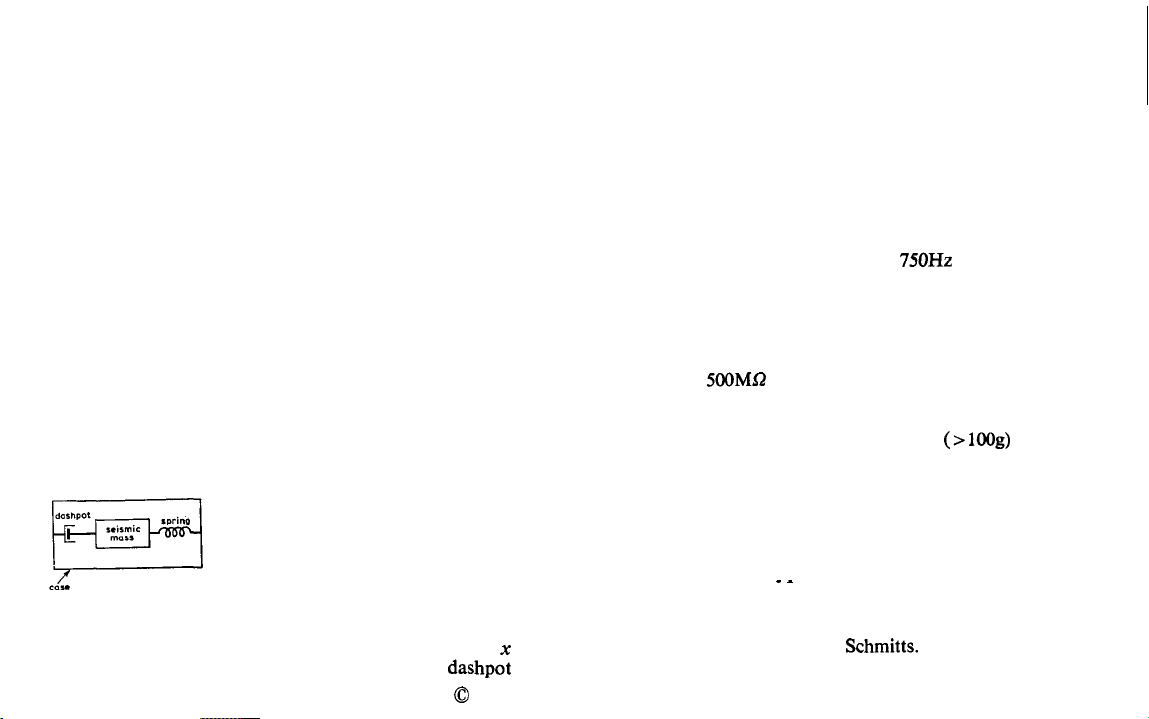
Acceleration transducers all have one feature in common viz
the seismic mass, M. The basic acceleration transducer is
shown below. The case of the system is attached to the
body whose acceleration is required. Due to a constant
acceleration the seismic mass exerts a force MU which in the
steady state will stretch or compress the spring by an amount
where Ma = Kx, K being the spring constant. The dashpot
x
0
1974 JPC Business Press Ltd.
simply provides damping whilst the mass is moving. If we
know M and K then a measure of x gives a signal proportional
to the acceleration. This can be done by any displacement
transducer of suitable dimensions and sensitivity. Frequently,
however, the spring arrangement is a leaf spring arrangement
with strain gauges attached. The spring deflection gives rise
to changes in resistance in the strain gauges which if connected in a Wheatstone bridge circuit gives a voltage proportional to the deflection and, hence, to the acceleration. As the
Wheatstone bridge can be supplied from a d.c. source there
is no need for rectifiers before feeding to a comparator.
Strain gauge bridges usable up to
For higher frequencies piezoelectric crystals replace the
spring. The crystal produces a charge or voltage across its
terminals when subjected to the stress of the seismic mass
under acceleration. However, the output impedance of the
crystal is large and amplifiers with an input impedance in
excess of
cable between the crystal and the amplifier requires to have
low capacitance and to be free from friction induced noise. On
the other hand very large accelerations (>
sured and they can be used over a large temperature range
(570°C for a lead metaniobate crystal).
5OOMO
typically have to be. used. Furthermore, the
75OHz
have been built.
1OOg)
can be mea-
Further reading
H. N. Norton, Handbook of Transducers for Electronic
Measuring Systems, Prentice-Hall.
Considine. Encvclonedia of Instrumentation and Control.
McGraw&ill. -
_
Cross references
Series 2, Comparators and
Series 4, A.C. Measurements.
Schmitts.
Series 13, card 4.
 Loading...