

AKM AKD5354 Datasheet
ASAHI KASEI [AKD5354]
AKD5354
Evaluation board Rev.A for AK5354
GENERAL DESCRIPTION
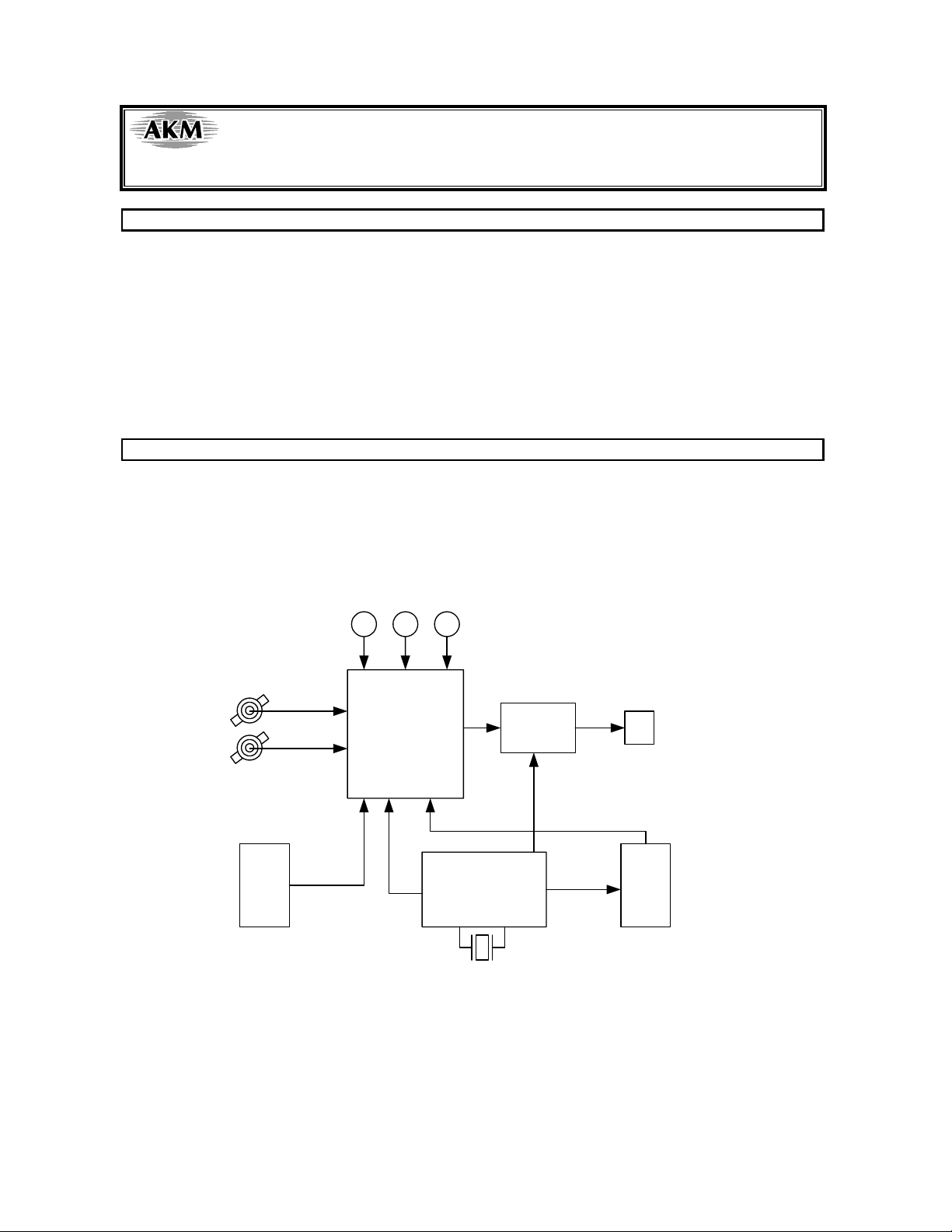
AKD5354 is an evaluation board for the portable digital audio 20bit A/D converter, AK5354. The
AKD5354 includes the input circuit and also has a digital interface transmitter. Further, the AKD5354 can
evaluate direct interface with AKM’s D/A converter evaluation board.
n Ordering guide
AKD5354 --- Evaluation board for AK5354
(Cable for connecting with printer port of IBM-AT,
compatible PC and control software are packed with this.)
FUNCTION
• Compatible with 2 types of interface
- Direct interface with AKM’s D/A converter evaluation boards
- On-board AK4353 as DIT which transmits optical output
• BNC connector for an external clock input
LIN1/2
RIN1/2
Control
Data
10pin Header
* Circuit diagram and PCB layout are attached at the end of this manual.
GND
VDVA
AK4353
AK5354
(DIT)
Clock
Generator
Figure 1. AKD5354 Block Diagram
Opt Out
D/A Data
ROM Data
10pin Header
<KM062600> ’00/06
- 1 -
ASAHI KASEI [AKD5354]
1. Evaluation Board Manual
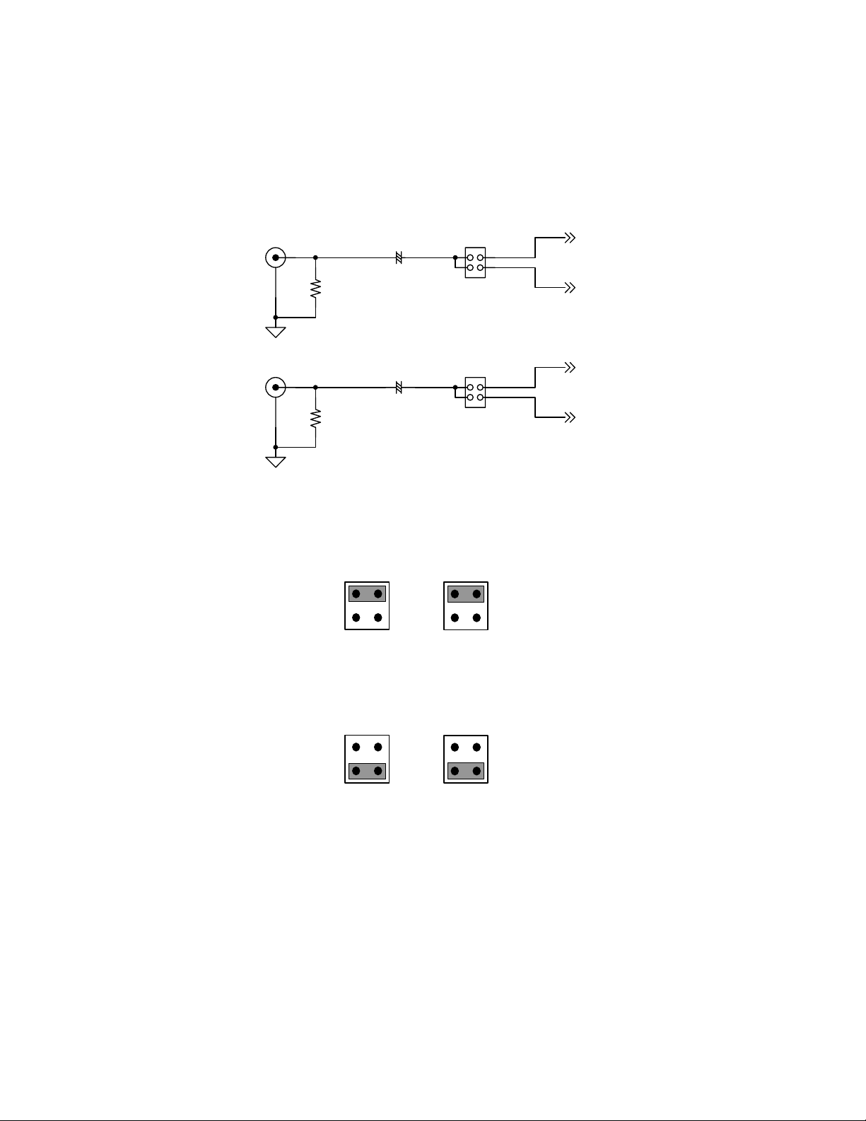
n Input circuit & Set-up jumper pin for Input circuits
(1) LINE Block
(a) LIN1,2/RIN1,2 Input circuit
J1
LIN
J2
RIN
R1
560
R3
560
C1
10u
+
C3
10u
+
JP1
LIN
JP2
RIN
LIN1
LIN2
RIN1
RIN2
Figure 2. LIN1,2/RIN1,2 Input circuit on board
1. Analog signal is input to LIN1 and RIN1 pins via J1 and J2 connectors.
JP1
LIN
LIN1
LIN2
JP2
RIN
RIN1
RIN2
LIN1
LIN2
RIN1
RIN2
2. Analog signal is input to LIN2 and RIN2 pins via J1 and J2 connectors.
JP1
LIN
LIN1
LIN2
JP2
RIN
RIN1
RIN2
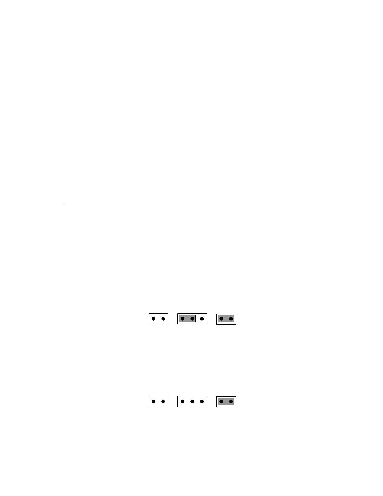
(2) Other Jumper pins
1. JP3 (VD) : VD of AK5354
VA : Supplied from “VA” connector via 10Ω.
VD : Supplied from “D2V” connector.
2. JP4 (GND) : Analog ground and Digital ground
open : separated
short : common (The connector “DGND” can be open.)
* AKM assumes no responsibility for the trouble when using the circuit examples.
<KM062600> ’00/06
- 2 -
ASAHI KASEI [AKD5354]
n Operation sequence
1) Set up the power supply lines.
[VA] (orange) = 2.2 ∼ 3.3V : for VA of AK5354 (typ. 2.5V)
[D2V] (orange) = 1.8 ∼ 3.3V : for D2V of 74LVC541 (typ. 2.5V)
[VCC] (red) = 3.6 ∼ 5.0V : for logic
[AGND] (black) = 0V : for analog ground (including VSS of AK5354)
[DGND] (black) = 0V : for logic ground
Each supply line should be distributed from the power supply unit.
D2V and VA must be same voltage level.
2) Set up the evaluation mode, jumper pins and DIP switches. (See the followings.)
2
Note : Evaluation mode of the AK5354 is fixed to I
S compatible on the board.
3) Power on.
The AK5354 and AK4353 should be reset once bringing SW1 = SW2 = “L” upon power-up.
n Evaluation mode
Applicable Evaluation Mode
(1) Evaluation of A/D using DIT (Optical Link)
(2) Evaluation of A/D using D/A converted data
(3) All interface signals including master clock are fed externally.
(1) Evaluation of A/D using DIT (Optical Link)
PORT1 (DIT) is used. DIT generates audio bi-phase signal from received data and which is output through
optical connector (TOTX176). It is possible to connect AKM’s D/A converter evaluation boards on the digitalamplifier which equips DIR input. Nothing should be connected to PORT3 (ROM). In case of using external
clock through a BNC connector (J3), select EXT on JP6 (CLK) and short JP5 (XTE) and open JP7 (EXT).
JP5
XTE
JP6
CLK
EXTXTL
JP7
EXT
(2) Evaluation of A/D using D/A converted data
It is possible to make evaluation in the form of analog inputs and analog outputs by interfacing with various
AKM’s D/A evaluation boards with PORT3 (ROM).
JP5
XTE
JP6
CLK
JP7
EXT
EXTXTL
<KM062600> ’00/06
- 3 -
ASAHI KASEI [AKD5354]
(3) All interface signals including master clock are fed externally.
Under the following set-up, all external signals needed for the AK5354 to operate could be fed through PORT3
(ROM).
JP5
XTE
n The function of the toggle SW
Upper-side is “H” and lower-side is “L”.
[SW1] (PDN): Resets the AK5354. Keep “H” during normal operation.
[SW2] (DIT): Resets the AK4353. Keep “H” during normal operation.
n Serial Control
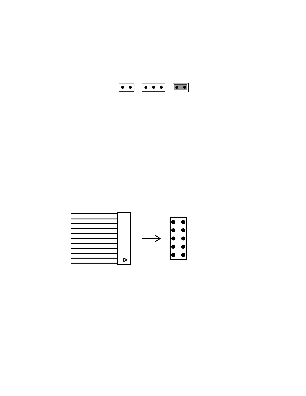
The AK5354 can be controlled via the printer port (parallel port) of IBM-AT compatible PC. Connect
PORT2(CTRL) with PC by 10-line flat cable packed with the AKD5354.
Take care of the direction of connector. There is a mark pin#1 to connector.
JP6
CLK
EXTXTL
JP7
EXT
PC
10 wire
flat cable
Connect
10pin
10pin Header
Connector
Figure 3. Connect of 10-line flat cable
CSN
CCLK
CDTI
AKD5354
<KM062600> ’00/06
- 4 -

ASAHI KASEI [AKD5354]
2. Control Software Manual
n Set-up of evaluation board and control software
1. Set up the AKD5354 according to previous term.
2. Connect IBM-AT compatible PC with AKD5354 by 10-line type flat cable (packed with AKD5354). Take care of the
direction of 10pin header. (This control software does not operate on Windows NT, therefore please operate it on
Windows95/98.)
3. Insert the floppy-disk labeled “AKD5354 Control Program ver 1.0” into the floppy-disk drive.
4. Access the floppy-disk drive and double-click the icon of “akd5354.exe” to set up the control program.
5. Then please evaluate according to the follows.
n Explanation of each buttons
1. [Port Setup] : Set up the printer port.
2. [Write default] : Initialize the register of AK5354.
3. [Function1] : Dialog to write data by keyboard operation.
4. [Function2] : Dialog to evaluate IPGA.
5. [Write] : Dialog to write data by mouse operation.
Note : It is necessary to MCLK=256fs and I
Because AK4353 is fixed to MCLK=256fs and I
2
S for audio data format in the beginning.
2
S for audio data format.
<KM062600> ’00/06
- 5 -

ASAHI KASEI [AKD5354]
n Explanation of each dialog
1. [Function1 Dialog] : Dialog to write data by keyboard operation
Address Box: Input register address in 2 figures of hexadecimal.
Data Box: Input register data in 2 figures of hexadecimal.
If you want to write the input data to AK5354, click “OK” button. If not, click “Cancel” button.
2. [Function2 Dialog] : Dialog to evaluate IPGA
This dialog corresponds to only addr=03H.
Address Box: Input register address in 2 figures of hexadecimal.
Start Data Box: Input start data in 2 figures of hexadecimal.
End Data Box: Input end data in 2 figures of hexadecimal.
Interval Box: Data is written to AK5354 by this interval.
Step Box: Data changes by this step.
Mode Select Box:
If you check this check box, data reaches end data, and returns to start data.
[Example] Start Data = 00, End Data = 09
Data flow: 00 01 02 03 04 05 06 07 08 09 09 08 07 06 05 04 03 02 01 00
If you do not check this check box, data reaches end data, but does not return to start data.
[Example] Start Data = 00, End Data = 09
Data flow: 00 01 02 03 04 05 06 07 08 09
If you want to write the input data to AK5354, click “OK” button. If not, click “Cancel” button.
3. [Write Dialog] : Dialog to write data by mouse operation
There are dialogs corresponding to each register.
Click the “Write” button corresponding to each register to set up the dialog. If you check the check box, data becomes
“H” or “1”. If not, “L” or “0”.
If you want to write the input data to AK5354, click “OK” button. If not, click “Cancel” button.
n Operation flow
Keep the following flow surely.
1. Set up the control program according to explanation above.
2. Click “Port Setup” button.
3. Click “Write default” button.
4. Then set up the dialog and input data.
<KM062600> ’00/06
- 6 -
 Loading...