

AKM AKD4364 Datasheet
ASAHI KASEI [AKD4364]
AKD4364
Evaluation board Rev.A for AK4364
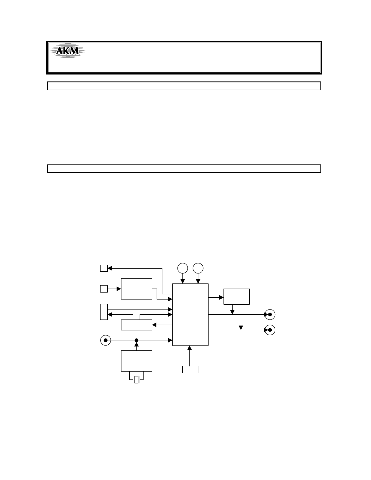
GENERAL DESCRIPTION
The AKD4364 is an evaluation board for AK4364, 96kHz 24bit D/A converter with PLL & DIT. The
AKD4364 has a digital interface with AKM’s wave generator using ROM data and AKM’s A/D converter
evaluation boards. Therefore, it is easy to evaluate the AK4364.
n Ordering guide
AKD4364 --- Evaluation board for AK4364
(Cable for connecting with printer port of IBM-AT compatible PC
and control software are packed with this.)
FUNCTION
• On-board clock generator
• Compatible with 2 types of interface
- Direct interface with AKM’s A/D converter evaluation boards
and direct interface with AKM’s signal generator(AKD43XX) by 10pin header
- On-board CS8414 as DIR which accepts optical input
• BNC connector for external clock input
• 10pin header for serial control interface
• On-board mute circuit for analog output
• Optical output for TX output
Opt Out
Opt In
ROM
or A/D
10pin Header Divider
External
Clock
* Circuit diagram and PCB layout are attached at the end of this manual.
CS8414
(DIR)
Clock
Generator
Figure 1. AKD4364 Block Diagram
2.7∼5.5V GND
AK4364
MCKO
MCKI
Control
DZF
Mute
Lch
Rch
10pin Header
<KM061301> ’00/4
- 1 -
ASAHI KASEI [AKD4364]
n External analog circuit
J1(AOUTL) and J2(AOUTR) are used. The analog output signal range is nominally 3.1Vpp@5V. It is proportional
to AVDD (Vout=0.62xAVDD).
n Operation sequence
1) Set up the power supply lines.
[AVDD] (red) = 2.7∼5.5V : for AVDD of AK4364
[3V] (orange) = 2.7∼5.5V : for DVDD of AK4364
[5V] (red) = 3.4∼5.5V : for logic
[AGND] (black)= 0V : for analog ground (including AVSS and DVSS of AK4364)
[DGND] (black)= 0V : for logic ground
Each supply line should be distributed from the power supply unit.
2) Set up the evaluation mode, jumper pins and DIP switches. (See the followings.)
3) Power on.
The AK4364 should be reset once bringing SW1(-PD) “L” upon power-up.
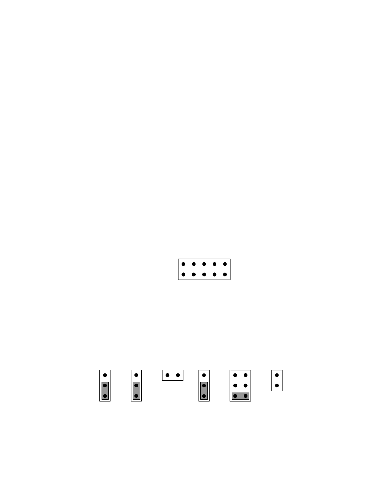
4) Connect PORT2 with PC.
Connect PORT2 with printer port (parallel port) of IBM-AT compatible PC by 10-line flat cable packed with
the AKD4364. Take care of the direction of connector. There is a mark at 1pin. The direction of PORT2 is as
the following figure.
5) Set up the software.
Use the software named “AKD4364 Control Program” packed with the AKD4364.
n Evaluation mode
1) Using A/D converted data <default>
PORT3 (ADC/ROM) is used to interface with various AKM’s A/D converter evaluation boards. In case of
using external clock through a BNC connector (J4), select BNC on JP14 (CLK) and short JP15 (XTE).
JP6
LRCK
BICK
DIR
ADC
JP7
PORT2
CTRL
DIR
ADC
9
10
JP12
DIR_DATA
-CS
SCL/CCLK
JP13
SDA/CDTI
DIR
VD
GND
SDA(ACK)
1
2
JP14
CLK
JP15
XTE
DIR
BNC
XTL
<KM061301> ’00/4
- 2 -

ASAHI KASEI [AKD4364]
2) Ideal sine wave generated by ROM data
Digital signals generated by AKD43XX are used. PORT3 (ADC/ROM) is used to interface with AK43XX.
Master clock is sent from AKD4364 to AKD43XX and LRCK, BICK, SDTI are supplied from AKD43XX to
AKD4364. In case of using external clock through a BNC connector (J4), select “BNC” on JP14 (CLK) and
short JP15 (XTE).
JP6
LRCK
JP7
BICK
JP12
DIR_DATA
JP13
DIR
JP14
CLK
JP15
XTE
JP7
BICK
DIR
ADC
DIR
ADC
JP12
DIR_DATA
VD
GND
JP13
DIR
VD
GND
DIR
ADC
3) DIR(CS8414)
PORT4 (TORX174) is used for the evaluation using such as test disk. The DIR generates MCKI, BICK,
LRCK, SDTI from the received data through optical connector. In this case, the EXT bit of AK4364 should be
“1” (External clock mode). Select “RCA” or “OPT” on JP16 (RCA/OPT) in case of using RCA connector (J3)
or optical connector (PORT4: TORX174).
JP6
LRCK
DIR
ADC
n Clock (MCLK,BICK,LRCK) set up
In case of using evaluation mode 1), JP9,10 and 17 should be set up as follows.
They need no care for other evaluation mode.
JP14
CLK
DIR
BNC
XTL
JP15
XTE
DIR
BNC
XTL
MCLK JP9
(X_MCLK)
128fs x1 x1/128 32fs
256fs x1 x1/256 32fs
512fs x2 x1/256 32fs
1024fs x4 x1/256 32fs
Table 1. Clock set up
<KM061301> ’00/4
JP10
(X_LRCK)
BICK JP17
(X_BICK)
x1/4
64fs
128fs
64fs
128fs
64fs
128fs
64fs
128fs
- 3 -
x1/2
x1
x1/8
x1/4
x1/2
x1/8
x1/4
x1/2
x1/8
x1/4
x1/2
default
ASAHI KASEI [AKD4364]
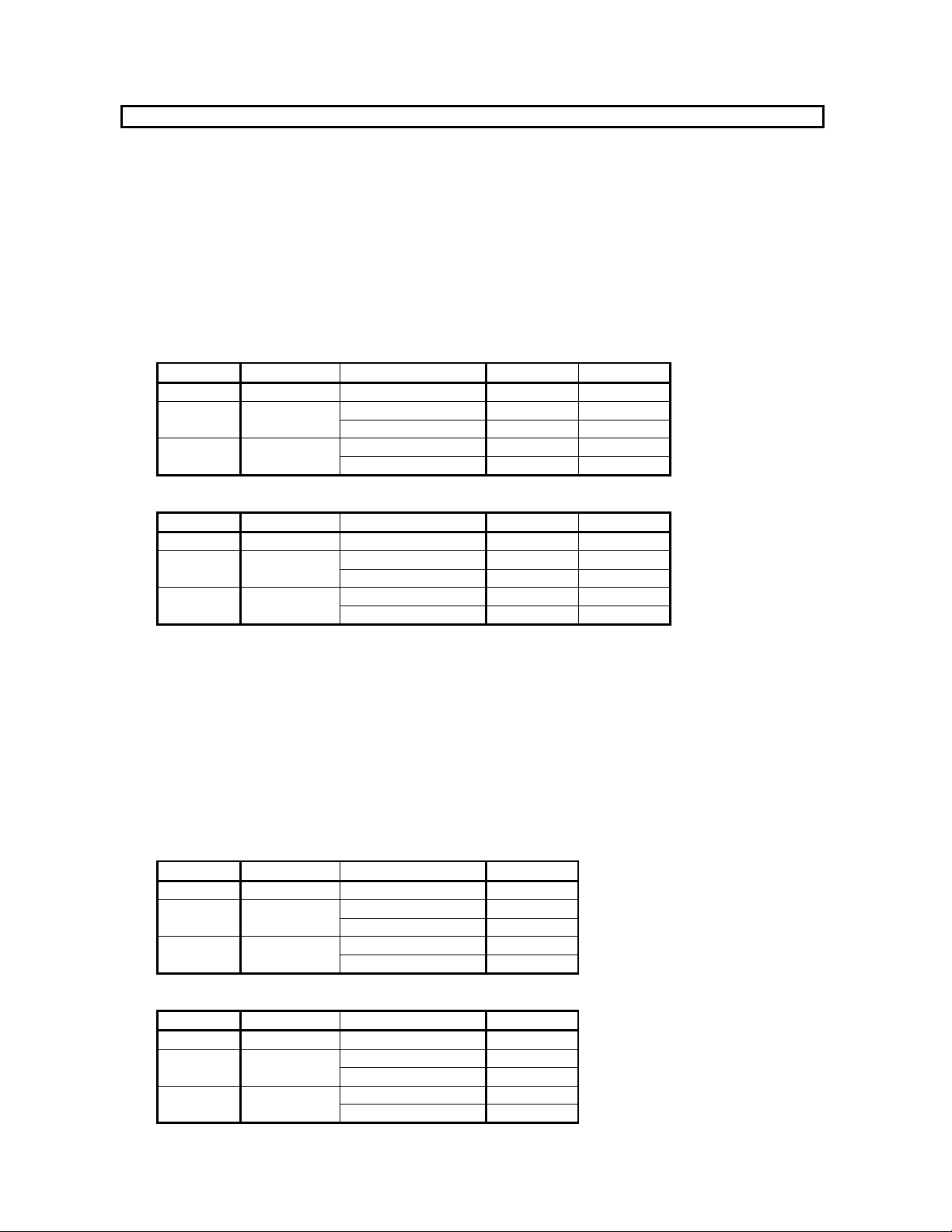
n DIP switch (SW2) set up
No.1 to 5 set the mode of AK4364 and No.6 to 8 set the mode of CS8414.
No. Pin OFF <default> ON
1 CAD1
2 CAD0
3 I2C 3-wire serial I2C bus
4 TTL CMOS level TTL level
5 TST always “OFF” 6M2
7M1
8M0
Table 2. DIP switch set-up
(Note: M2-0 should be selected at only evaluation mode 3.
In other mode, these should be “OFF”.)
Mode Format M2 M1 M0 JP9 DIF2 DIF1 DIF0
0 16bit, LSB justified 1 0 1 THR 0 0 0
1 18bit, LSB justified 1 1 0 THR 0 0 1
2 20bit, LSB justified ----010
3 24bit, LSB justified ----011
4 24bit, MSB justified 0 0 0 INV 1 0 0
5 I2S 010THR101
(Note: 1=”ON”, 0 = ” OFF”.
DIF2-0 should be selected by serial control.
CS8414 does not correspond to 20/24bit LSB justified format.)
Digital interface format of CS8414
Table 3. Digital interface format set-up
Chip address (2bit)
(See table 3.)
(Note)
n Serial control mode
The AK4364 can be controlled via the printer port (parallel port) of IBM-AT compatible PC. Connect PORT2
(CTRL) with PC by 10-line flat cable packed with the AKD4364.
There are two modes: 3-wire serial & I2C bus. JP4 should be shorted at 3-wire serial control mode.
Chip address can be selected by SW2(MODE)-No.1(CAD1) and No.2(CAD0).
n Other jumper pins set up
[JP1](GND): Analog ground and digital ground
Open: Separated <default>
Short: Common (The connector “DGND” can be open.)
[JP2](5V-3V): DVDD of AK4364 and power supply to logic
Open: Independent <default>
Short: Same (The connector “3V” should be open.)
<KM061301> ’00/4
- 4 -

ASAHI KASEI [AKD4364]
[JP3](DVDD): DVDD of AK4364
3V: Independent of AVDD <default>
AVDD: Same as AVDD (The connector “3V” can be open.)
[JP5](DZF): Mute circuit
ON: Used (Analog output is muted when DZF=”H”.) <default>
OFF: Not used
[JP11](SDTI): SDTI of AK4364
DATA: Data is input <default>
GND: “0” data is input
n The function of the toggle SW (SW1)
Upper-side is “H” and lower-side is “L”.
[SW1] (-PD):Resets th e AK4364. Keep “H” during normal operation.
n The indication content for LED
[LED1] (VERF): Monitors VERF pin of the CS8414. LED turns on when some error has occurred to CS8414.
[LED2] (PREM): Indicates whether the input data is pre-emphasis or not.
LED turns on when the data is pre-emphasised.
<KM061301> ’00/4
- 5 -
ASAHI KASEI [AKD4364]
MEASUREMENT RESULTS
[Measurement condition]
• Measurement unit : ROHDE & SCHWARZ, UPD04
• MCLK : 256fs
• BICK : 64fs
• fs : 44.1kHz, 96kHz
• BW : 20Hz∼20kHz (fs=44.1kHz), 20Hz∼40kHz (fs=96kHz)
• Bit : 24bit
• Power Supply : AVDD=DVDD=5V
• Interface : DIR (EXT mode, fs=44.1kHz), Serial Multiplex (EXT mode, fs=96kHz; PLL mode)
• Temperature : Room
fs=44.1kHz
Parameter Input signal Measurement filter EXT PLL
S/(N+D) 1kHz, 0dB 20kLPF 97.0dB 88.9dB
20kLPF 99.0dB 98.4dBDR 1kHz, -60dB
20kLPF, A-weighted 102.3dB 101.9dB
20kLPF 99.0dB 98.4dBS/N no signal
20kLPF, A-weighted 102.3dB 101.9dB
fs=96kHz
Parameter Input signal Measurement filter EXT PLL
S/(N+D) 1kHz, 0dB 40kLPF 92.5dB 84.9dB
40kLPF 97.0dB 95.9dBDR 1kHz, -60dB
20kLPF, A-weighted 101.5dB 101.9dB
40kLPF 97.0dB 95.9dBS/N no signal
20kLPF, A-weighted 101.5dB 101.9dB
[Measurement condition]
• Measurement unit : Audio Precision, System two, Cascade
• MCLK : 256fs
• BICK : 64fs
• fs : 44.1kHz, 96kHz
• BW : 10Hz∼20kHz (fs=44.1kHz), 10Hz∼40kHz (fs=96kHz)
• Bit : 24bit
• Power Supply : AVDD=DVDD=5V
• Interface : DIR
• Temperature : Room
fs=44.1kHz
Parameter Input signal Measurement filter EXT
S/(N+D) 1kHz, 0dB 20kLPF 97.4dB
20kLPF 98.8dBDR 1kHz, -60dB
22kLPF, A-weighted 101.6dB
20kLPF 98.6dBS/N no signal
22kLPF, A-weighted 101.8dB
fs=96kHz
Parameter Input signal Measurement filter EXT
S/(N+D) 1kHz, 0dB 40kLPF 94.5dB
40kLPF 96.9dBDR 1kHz, -60dB
22kLPF, A-weighted 101.9dB
40kLPF 96.8dBS/N no signal
22kLPF, A-weighted 101.9dB
<KM061301> ’00/4
- 6 -

ASAHI KASEI [AKD4364]
PLOTS
[Measurement condition]
• Measurement unit : ROHDE & SCHWARZ, UPD04 (for PLL mode),
Audio Precision, System two (for EXT mode)
• MCLK : 256fs
• BICK : 64fs
• fs : 44.1kHz, 96kHz
• Bit : 24bit
• Power Supply : AVDD=DVDD=5V
• Interface : Serial Multiplexer (for PLL mode), DIR (for EXT mode)
• Temperature : Room
[Contents]
1. PLL mode
1-1. fs=44.1kHz
Figure 1-1-1. THD+N vs. Input level
Figure 1-1-2. THD+N vs. Input frequency
Figure 1-1-3. Linearity
Figure 1-1-4. Frequency response
Figure 1-1-5. Cross-talk
Figure 1-1-6. FFT (1kHz, 0dBFS)
Figure 1-1-7. FFT (1kHz, -60dBFS)
Figure 1-1-8. FFT (noise floor)
Figure 1-1-9. FFT (out-of-band noise, ∼300kHz)
1-2. fs=96kHz
Figure 1-2-1. THD+N vs. Input level
Figure 1-2-2. THD+N vs. Input frequency
Figure 1-2-3. Linearity
Figure 1-2-4. Frequency response
2. EXT mode
2-1. fs=44.1kHz
Figure 2-1-1. THD+N vs. Input level
Figure 2-1-2. THD+N vs. Input frequency
Figure 2-1-3. Linearity
Figure 2-1-4. Frequency response
Figure 2-1-5. Cross-talk
Figure 2-1-6. FFT (1kHz, 0dBFS)
Figure 2-1-7. FFT (1kHz, -60dBFS)
Figure 2-1-8. FFT (noise floor)
Figure 2-1-9. FFT (out-of-band noise, ∼80kHz)
2-2. fs=96kHz
Figure 2-2-1. THD+N vs. Input level
Figure 2-2-2. THD+N vs. Input frequency
Figure 2-2-3. Linearity
Figure 2-2-4. Frequency response
<KM061301> ’00/4
- 7 -
ASAHI KASEI [AKD4364]
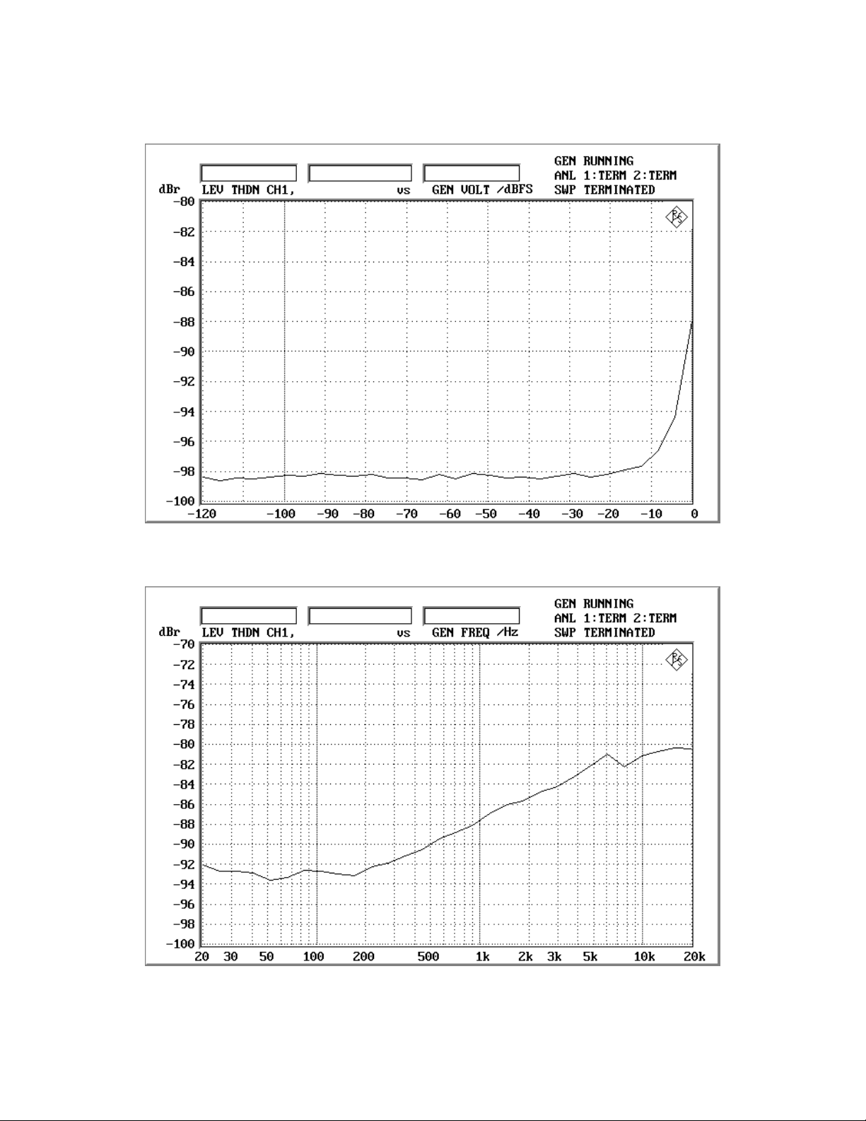
1. PLL mode
1-1. fs=44.1kHz
Figure 1-1-1. THD+N vs. Input level
Figure 1-1-2. THD+N vs. Input frequency
<KM061301> ’00/4
- 8 -
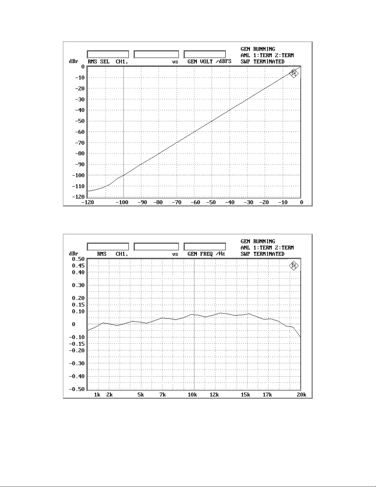
ASAHI KASEI [AKD4364]
Figure 1-1-3. Linearity
Figure 1-1-4. Frequency response
<KM061301> ’00/4
- 9 -
 Loading...