

AKM AK9824M, AK9822M Datasheet
ASAHI KASEI [AK9822/24]
AK9822 / 24
2K / 4Kbit EEPROM with 2ch 8bit D/A Converter
General Description
The AK9822/24 includes 2 channel, 8 bit D/A convert ers wit h on-chip output buffer amps and it is
capable to store the input digital data of each D/A converter by on-chip non-volatile CMOS
EEPROM. The AK9822/24 is optimally designed for various circuit adjustments for consumer and
industrial equipments and it is ideally suited for replacing mechanical trimmers.
Feature
EEPROM section
• • •
AK9822
AK9824
One chip microcomputer interface
Sequential register read
128 words Õ 16bit
• • •
256 words Õ 16bit
D/A Converter section
2 channel
Resolution : 8bit
Differential Non-Linearity : 1.0 LSB
Linearity Error : 1.5 LSB
Output Voltage Range : GND ∼ VCC
Wide VCC operation
•
EEPROM section : 1.8V∼5.5V
•
D/A Converter Section : 2.7V∼5.5V
Power Down Function
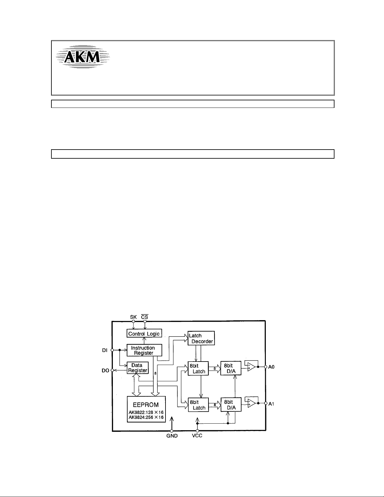
Block Diagram
DAD01E-00 1999/05
- 1 -
ASAHI KASEI [AK9822/24]
Ordering Guide
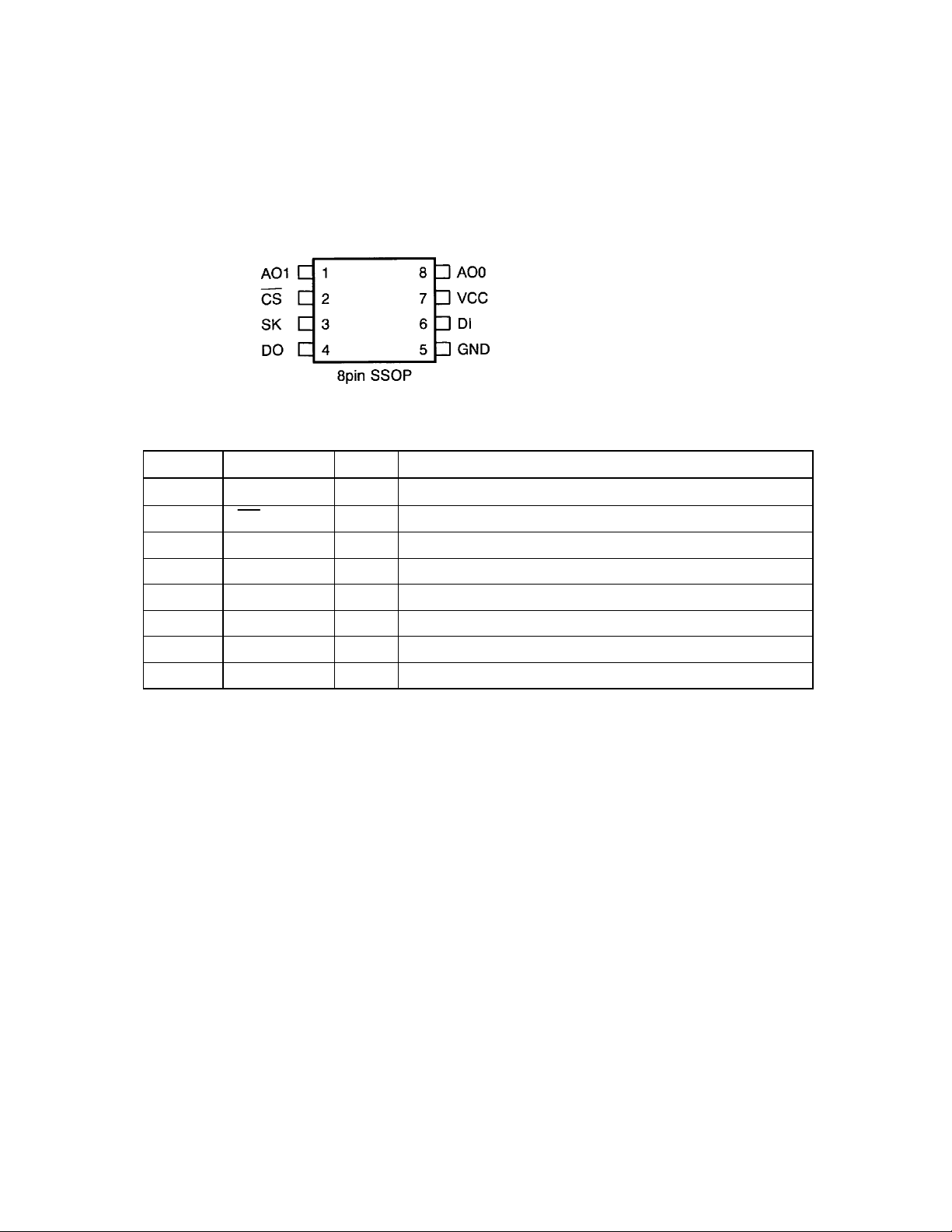
Pin Layout
Pin Description
AK9822M -40°C∼+85°C 8pin SSOP
AK9824M -40°C∼+85°C 8pin SSOP
No. Pin Name I/O Function
1 AO1 O Analog Output Pin
2 CS I Chip Select Pin (Schmitt-trigger input)
3 SK I Serial Clock Pin (Schmitt-tr igger input)
4 DO O Serial Data Output Pin
5 GND - Ground Pin
6 DI I Serial Data Input Pin
7 VCC - Power Supply
8 AO0 O Analog Output Pin
DAD01E-00 1999/05
- 2 -

ASAHI KASEI [AK9822/24]
Functional Description
The AK9822/24 is composed of EEPROM and the 8bit D/A converter of two channels with the
output buffer amplifier.
The AK9822/24 can connect to the serial communication port of popular one chip microcomputer
directly (3 line negative clock synchronous interface).
The AK9822/24 takes the data of the DI pin by the rising edge of the SK pin and outputs the data
from the DO pin by the falling edge of the SK pin.
The AK9822/24 has 7 instructions such as READ, WRITE, WREN, WRDS, PDEN, PDDS and CALL.
The AK9822/24 is operated by inputting these instructions from the serial interface. Each instruction
is organized by op-code block (8bits), address block (8bits) and data (8bitsÕ2).
The DO pin is "Hi-Z" state except that the DO pin outputs the data of the internal register and the
status of Ready/Busy.
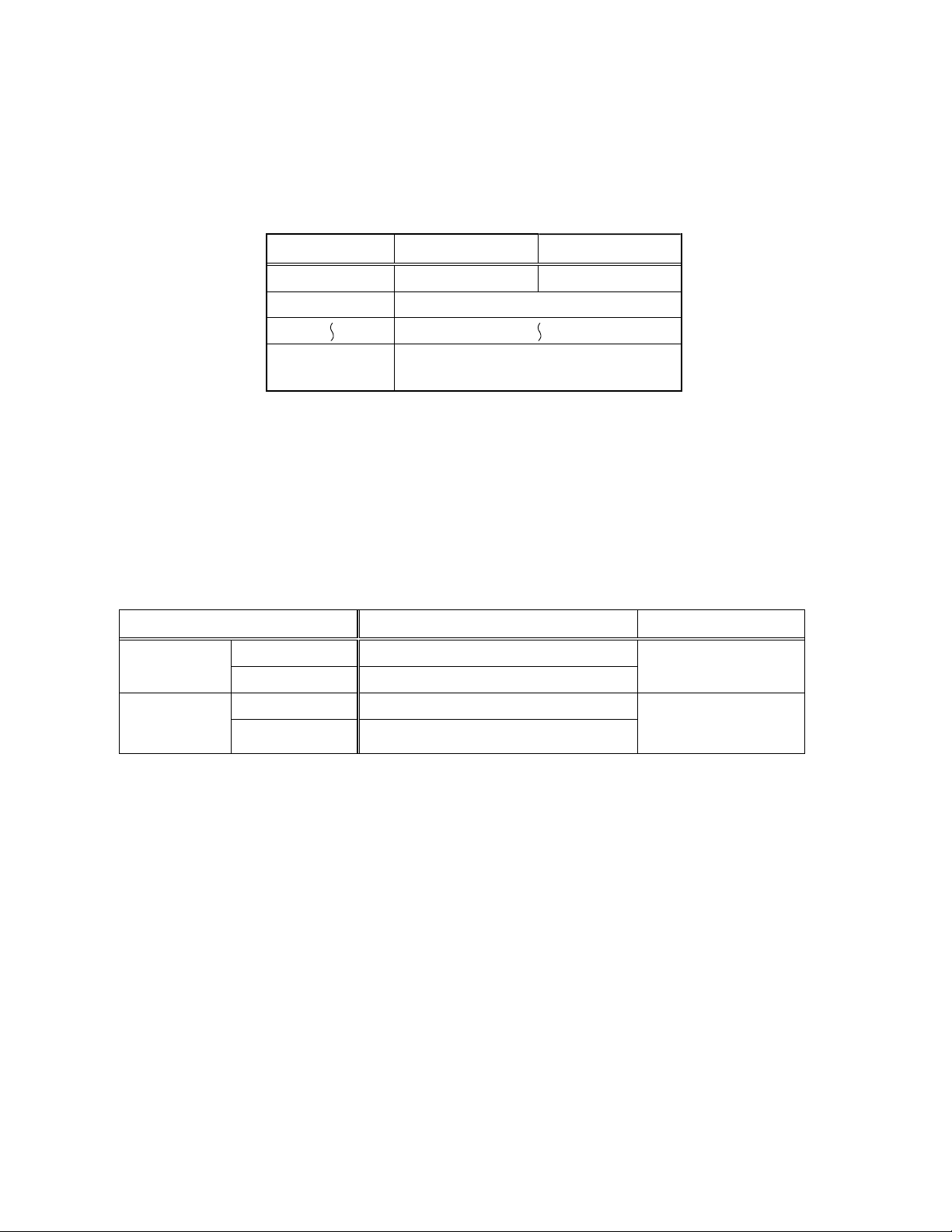
WRITE protection function
There are two states such as the WRITE enable state and the WRITE disable state in the
AK9822/24. In the WRITE disable state the WRITE instruction becomes invalid and is not executed.
When Vcc is applied to the part, the part powers up in the WRITE disable state and the part
becomes the WRITE enable state by inputting the WREN instruction. The WRITE enable state
continues until the WRDS instruction is executed or Vcc is removed from the part.
Execution of a READ instruction is independent of both WREN and WRDS instructions.
Power down function
There are two modes such as the power down mode and the normal mode in the AK9822/24. When
the AK9822/24 is in the power down mode, the D/A converter section is in the standby state. At this
time, the outputs of the D/A converters become "Hi-Z".
When Vcc is applied to the part, the AK9822/24 is in the power down mode. When a AUTO READ
function is executed, the part becomes the nor mal mode. After the AUTO READ function is
executed, the mode of the part can be switched by the PDEN and PDDS instructions. The
AK9822/24 becomes the power down mode by inputting the PDEN instruction. The part is in the
power down mode until the PDDS instruction is executed. When the PDDS instruction is executed,
the part becomes the normal mode.
When returning to the normal mode from the power down mode, the D/A converters output the
voltage value set before entering the power down mode. The relation between the D/A converter
state and the mode are shown in the table 1.
Mode State of D/A converter
Power down mode standby
Normal mode normal
Table 1. The relation between the state of D/A converter and the mode
DAD01E-00 1999/05
- 3 -
ASAHI KASEI [AK9822/24]
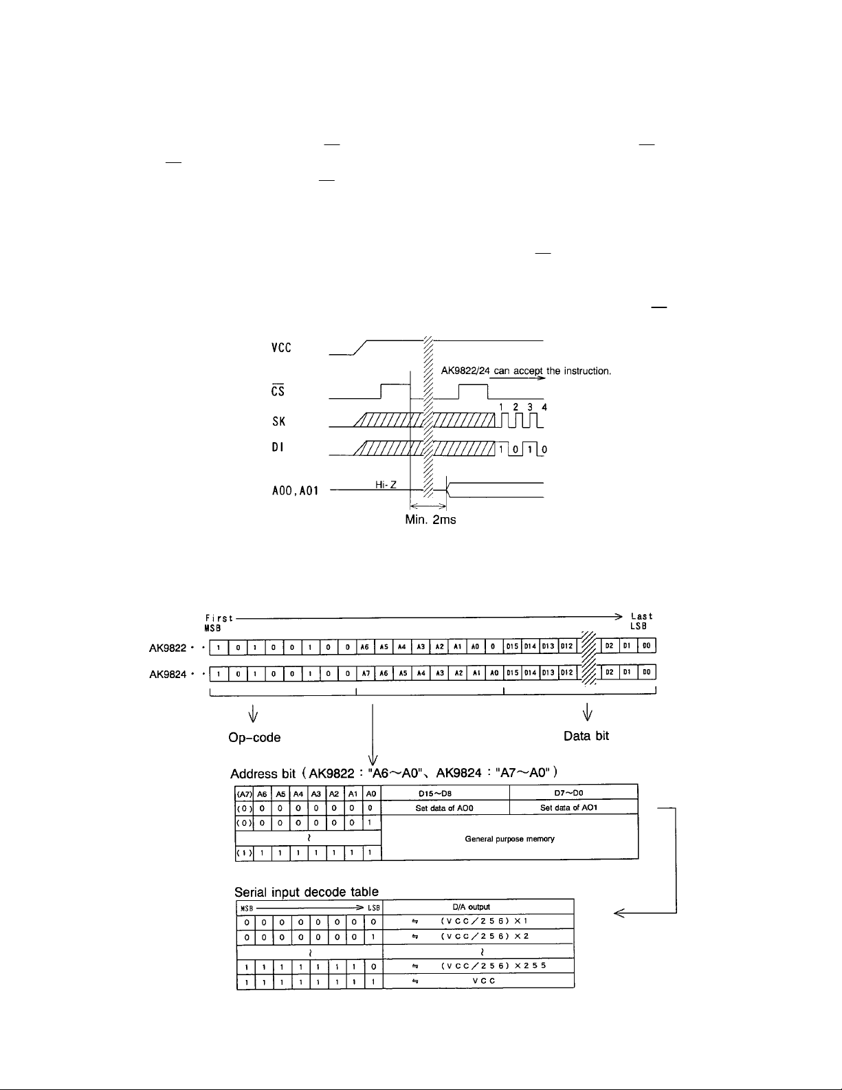
Output of D/A converter
The output of the D/A converters can be set by the WRITE and the CALL instructions.
Upper 8bit data (D15∼D8) of the first address of the internal EEPROM (the address "0")
corresponds to "AO" of the D/A converter output. Lower 8bit data (D7∼D0) of the address "0"
corresponds to "A1". The internal composition of EEPROM is shown in the table2.
Address
D15∼D8 D7∼D0
0 Set data of A0 Set data of A1
1 General purpose memory
127(AK9822)
General purpose memory
/255(AK9824)
Table2. Internal composition of EEPROM
If the WRITE instruction by which the address "0" is specified is executed at the normal mode, the
outputs of the D/A converter of A0 and A1 are set by the specified data.
When the WRITE instruction by which the address "0" is specified is executed at the WRITE enable
state and the normal mode, the data is written in the address "0" of EEPROM and the outputs of the
D/A converter are set. When the WRITE instr uction by which the address "0" is specified is
executed at the WRITE disable state and the normal mode, the data is not written in EEPROM and
the outputs of the D/A converter are set. Table3 shows the relation between EEPROM, D/A
converter and WRITE instruction.
State of AK9822/24 State of address"0" Output of A0 and A1
mode
WRITE enable The data change to the specified data.Power down
WRITE disable The data does not change.
WRITE enable The data change to the specified data.Normal mode
WRITE disable
The data does not change.
The DAC outputs
are "Hi-Z".
The DAC outputs
change to the
specified data.
Table3. Relation between EEPROM, D/A converter and WRITE instruction
If the CALL instruction is executed, the outputs of the D/A converter are set by the data of the
general purpose memory (AK9822:address "1" -"127", AK9824:address "1" -"255"). The CALL
instruction is composed by the op-code and the address.
When the CALL instruction is executed at the normal mode, the D/A converter output of A0 is set by
the upper 8bit data (D15∼D8) of the specified address and the output of A1 is set by the lower 8bit
data (D7∼D0). The CALL instruction is not executed at the power down mode.
DAD01E-00 1999/05
- 4 -
ASAHI KASEI [AK9822/24]
AUTO READ function
AUTO READ function automatically reads the content of EEPROM and sets the output of the D/A
converter of two channels, when Vcc is applied to the part.
When Vcc is applied to the part in CS="L", the AUTO READ function starts by falling CS pin first.
After the CS pin is made a low level, the output of AO0 and AO1 is set within 2ms. At this time, the
input pins (SK, DI) other than the CS pin are not accepted, and the serial data is not output from the
DO pin. If the WREN instruction is executed after the AUTO READ function finished, AK9822/24
becomes the WRITE enable state.
After Vcc is applied to the part, the AUTO READ function is executed only once.
AUTO READ function is executed when Vcc is applied to the part in CS="L".
(note) Because AK9822/24 always executes the AUTO READ function first after Vcc is applied to
the part, AK9822/24 is not able to accept the instruction for the first period of "L" of the CS.
Instruction and Composition of the data
Each instruction consist of op-code, address, and data (8bitÕ2) composed in each 8bit. The
composition of the WRITE instruction is shown as follows.
DAD01E-00 1999/05
- 5 -
ASAHI KASEI [AK9822/24]
Instruction Set
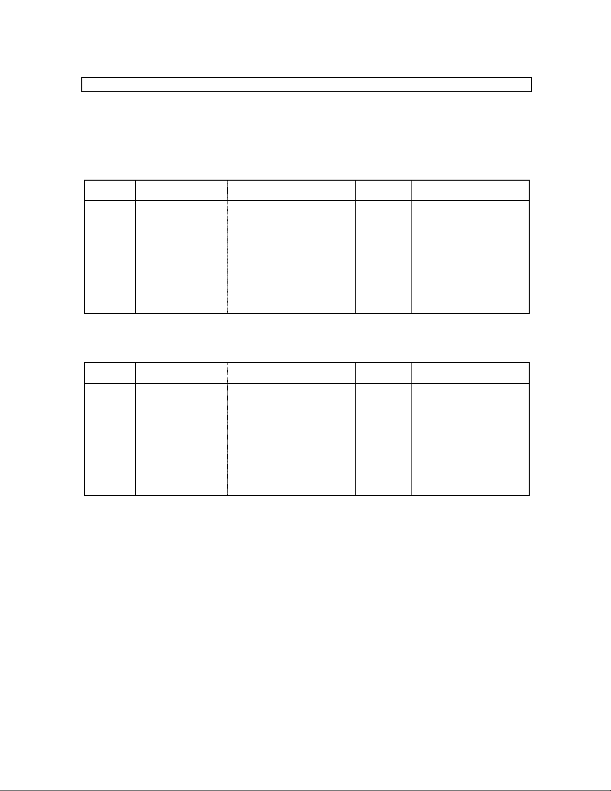
The AK9822/24 has 7 instructions such as READ, WRITE, WREN, WRDS, PDEN, PDDS, CALL.
Each instruction consists of Op-code, address and data. The instruction set is shown in the table4
and table5.
When the instructions are executed consecutively, the CS pin should be brought to a high level for a
minimum of tCS between consecutive instruction cycle.
Instruction Op-code Address Data Comments
READ
WRITE
WREN
WRDS
PDEN
PDDS
CALL
TEST
1 0 1 0 1 0 0 0
1 0 1 0 0 1 0 0
1 0 1 0 0 0 1 1
1 0 1 0 0 0 0 0
1 0 1 0 1 1 0 0
1 0 1 0 0 1 1 0
1 0 1 0 0 0 1 0
1 0 1 0 1 1 1 1
A6 A5 A4 A3 A2 A1 A0 0
A6 A5 A4 A3 A2 A1 A0 0
********
********
********
********
A6 A5 A4 A3 A2 A1 A0 0
********
D15∼D0
D15∼D0
∼
*
∼
*
∼
*
∼
*
∼
*
∼
*
read memory
write memory
write enable
write disable
power down enable
power down disable
set DAC outputs
TEST (note)
(note) User can't use this instruction. *: Don't Care
Table4. Instruction set for AK9822
Instruction Op-code Address Data Comments
READ
WRITE
WREN
WRDS
PDEN
PDDS
CALL
TEST
1 0 1 0 1 0 0 0
1 0 1 0 0 1 0 0
1 0 1 0 0 0 1 1
1 0 1 0 0 0 0 0
1 0 1 0 1 1 0 0
1 0 1 0 0 1 1 0
1 0 1 0 0 0 1 0
1 0 1 0 1 1 1 1
A7 A6 A5 A4 A3 A2 A1 A0
A7 A6 A5 A4 A3 A2 A1 A0
********
********
********
********
A7 A6 A5 A4 A3 A2 A1 A0
********
D15∼D0
D15∼D0
∼
*
∼
*
∼
*
∼
*
∼
*
∼
*
read memory
write memory
write enable
write disable
power down enable
power down disable
set DAC outputs
TEST (note)
(note) User can't use this instruction. *: Don't Care
Table5. Instruction set for AK9824
DAD01E-00 1999/05
- 6 -
 Loading...