

AKM AK7714 Datasheet
[ASAHI KASEI]
[AK7714]
AK7714
20-Bit Audio Codec with DSP and Dela y RAM
General Description
The AK7714 is a highly integrated audio processing IC with 20-bit stereo ADC and 4-channel DAC plus
on-chip DSP with 64-kbit delay RAM. The built-in ADC has a dynamic range of 99 dB with S/(N+D) of 92 dB,
and the DAC has a dynamic range of 98 dB with S/(N+D) of 89 dB, thereby ensuring high performances.
The AK7714 is compatible with each of the sampling frequencies of 48 kHz, 44.1 kHz or 32 kHz, and a
program of 512 steps (when sampling at 44.1 kHz or 32 kHz) can be executed in one sampling time. The
AK7714 is a programmable audio DSP containing RAM for delay. This allows sound field control programs to
be implemented for surround sound, echo 3D, parametric equalizer and the like.
Furthermore, the AK7714 uses a small 100-pin LQFP package, providing the optimum system for the sound
field of car audio equipment which is required to meet space saving requirements.
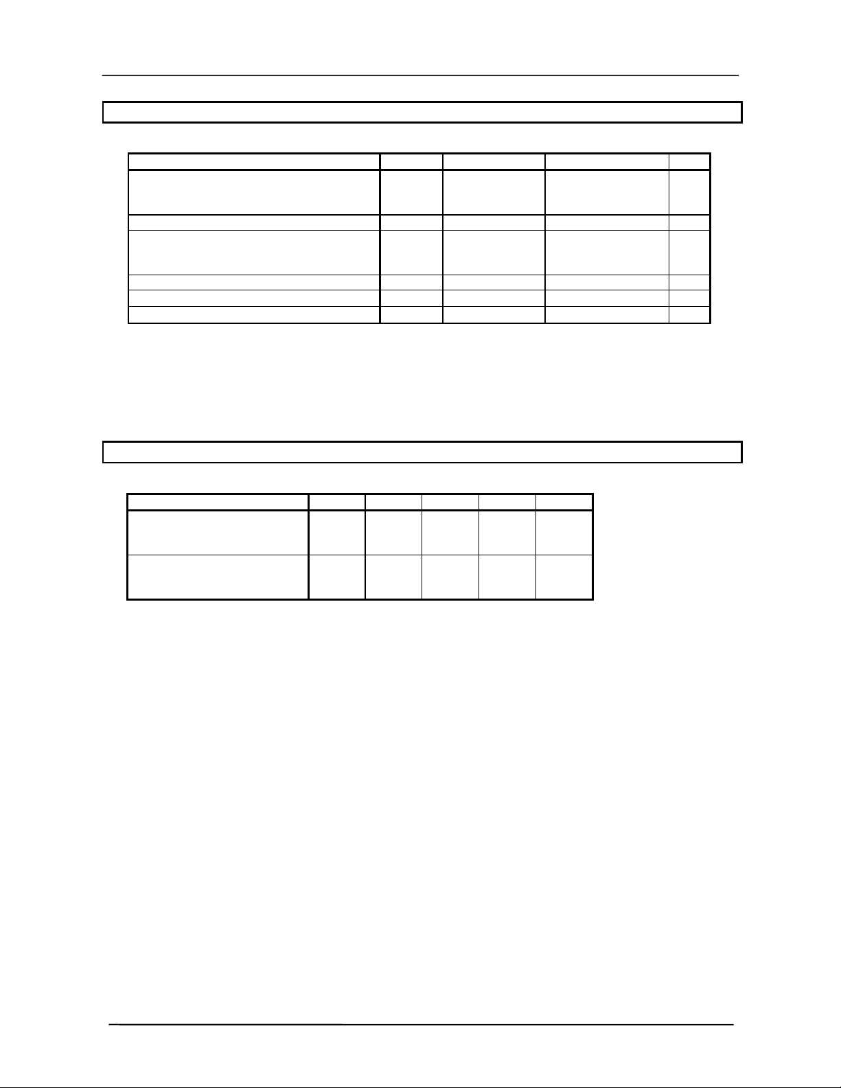
Features
DSP:
Word length: 24-bit (Data RAM)
-
Instruction cycle time: 44.2 ns
-
Multiplier: 24 x 16 40-bit
-
Divider: 24 / 24 16-bit
-
ALU: 34-bit arithmetic operation (Overflow margin: 4 bits)
-
24-bit arithmetic and logic operation
Shift+Register: 1, 2, 3, 4, 8 and 15 bits shifted left
-
1, 2, 3, 4, (6, 14), 8 and 15 bits shifted right
( )Numbers in parentheses are restricted.
Provided with indirect shift function
Program RAM: 448 x 32-bit
-
Coefficient RAM: 384 x 16-bit
-
Data RAM: 128 x 24-bit
-
Internal delay memory: 4096 x 16-bit or 2048 x 24-bit
-
Sampling frequency: 32 kHz to 48 kHz
-
Serial micro controller interface
-
Master clock: 512/384/256 fs (512 fs for sampling at 44.1 kHz or 32 kHz)
-
Master/slave operation
-
Serial signal input port (2 to 6 ch), output port (2 to 6 ch) : 16/20/24-bit
-
ADC: 2 channels
20-bit 64 x Over-sampling delta sigma
-
DR, S/N : 99 dB
-
S/(N+D) : 92 dB
-
Digital HPF (fc = 1 Hz)
-
DAC: 4 channels
20-bit 128 x Over-sampling delta sigma
-
DR, S/N : 98 dB
-
S/(N+D) : 89 dB
-
Others
Power voltage: + 5 V
-
Operating temperature range: -40
-
Package: 100-pin LQFP (0.5 mm pitch)
±±±±
5%
C to +85
°°°°
C
°°°°
M0018-E-00 ‘98/07
- 1 -

[ASAHI KASEI]
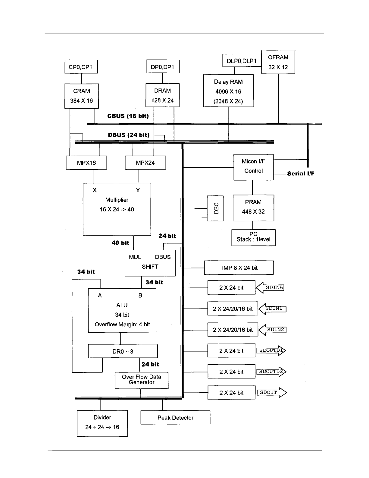
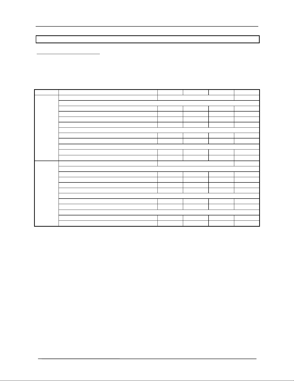
Block diagram
For standard operation (Internal connection mode, C3 t o C7: initial settings)
•
CPCL :L Internal connection mode
•
C3 ∼ C7 :All 0 (Initial settings)
[AK7714]
This block diagram is a simplified illustration of the AK7714; it is not a circuit diagram.
M0018-E-00 ‘98/07
- 2 -
[ASAHI KASEI]
Block Diagram of AK7714 DSP Section
[AK7714]
M0018-E-00 ‘98/07
- 3 -
[ASAHI KASEI]
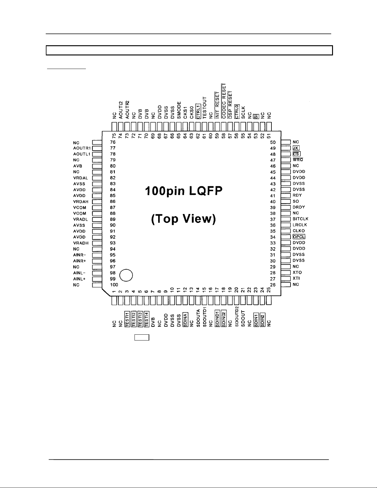
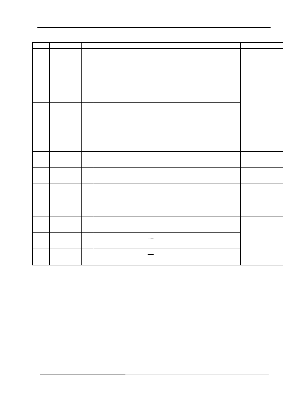
(1) Pin layout
[AK7714]
Description of Input/Output Pins
Note: Items enclosed i n boxes are provided with pulldown funct i ons.
M0018-E-00 ‘98/07
- 4 -
[ASAHI KASEI]
[AK7714]
(2) Pin function
Pin No. Pin name I/O Function Classification
Test pin: Leave open or connect to DVSS. (Pulldown)
3 TESTI1 I
Test pin: Leave open or connect to DVSS. (Pulldown)
4 TESTI2 I
Test pin: Leave open or connect to DVSS. (Pulldown)
5 TESTI3 I
Test pin: Leave open or connect to DVSS. (Pulldown)
6 TESTI4 I
Test
7 DVB -
9DVDD-
10,11 DVSS -
12 SDINA I
14 SDOUTA O
15 SDOUTD1 O
17 SDIND1 I
18 SDIND2 I
20 SDOUTD2 O
21 SDOUT O
+5 V power supply (Silicon substrate potential)
+5 V Digital power supply
Digital ground
DSP Serial data input pin (Pulldown)
OPCL="L": Disabled. Leave open or connect to DVSS.
OPCL="H": Compatible with MSB first 24 bits
ADC Serial data output pin
OPCL="L": Outputs "L".
OPCL="H": Outputs MSB first 20-bit data.
DSP Serial data output pin
OPCL="L": Outputs "L".
OPCL="H": Outputs MSB first 24-bit data.
DAC1 Serial data input pin (Pulldown)
OPCL="L": Disabled. Leave open or connect to DVSS.
OPCL="H": Compatible with MSB first 20 bits
DAC2 Serial data input pin (Pulldown)
OPCL="L": Disabled. Leave open or connect to DVSS.
OPCL="H": Compatible with MSB first 20 bits
DSP Serial data output pin
OPCL="L": Outputs "L".
OPCL="H": Outputs MSB first 24-bit data.
DSP Serial data output pin
Outputs MSB first 24-bit data.
Power supply
Digital section
Serial input/output
data
M0018-E-00 ‘98/07
- 5 -
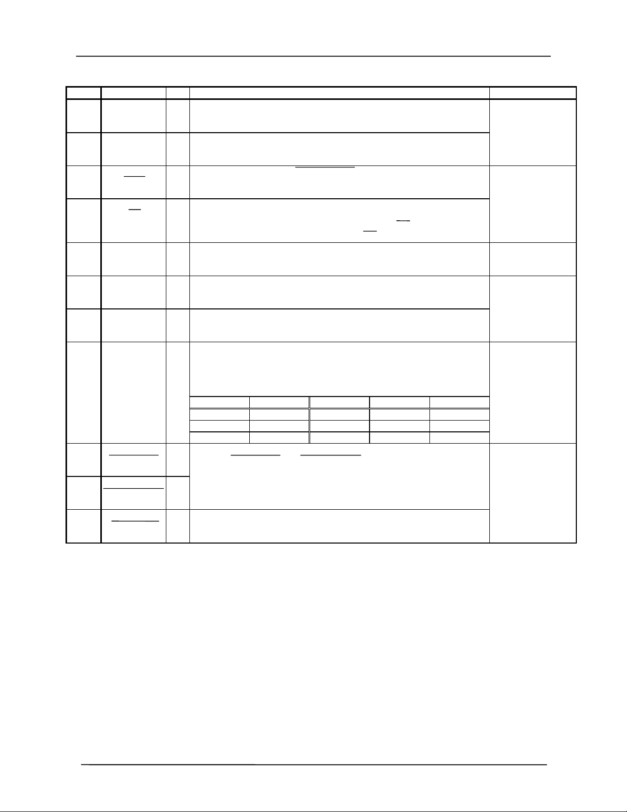
[ASAHI KASEI]
[AK7714]
Pin No. Pin name I/O Function Classification
Digital section
Serial input data
23 SDIN1 I
DSP Serial data input pin (Pulldown)
Compatible with MSB first/LSB first 24, 20 and 16 bits
DSP Serial data input pin (Pulldown)
24 SDIN2 I
Compatible with MSB first/LSB first 24, 20 and 16 bits
27 XTI I
28 XTO O
30,31 DVSS -
32,33 DVDD -
34 OPCL I
35 CLKO O
36 LRCLK I/O
37 BITCLK I/O
39 DRDY O
Master clock input pin
Connect a crystal oscillator between this pin and the XTO pin, or input the
external CMOS clock signal XTI pin. The clock frequency
can be selected by the CKS0 and CKS1 pins.
Crystal oscillator output pin
When a crystal oscillator is used, connect it between the XTI pin and this pin.
When the external clock is used, keep this pin open.
Digital Ground
+5 V Digital Power supply
ADC/DAC connection selector pin (Pulldown)
OPCL="L" (Leave open or connect to DVSS.): Connected
OPCL="H": Disconnected
Clock output pin
Outputs the XTI clock.
Allows the output to be set to "L" using the CTRL0 and CTRL1 pins.
LR channel select Clock pin
SMODE="L": Slave mode: Inputs the fs clock.
SMODE="H": Master mode: Outputs the fs clock.
Serial bit clock pin
SMODE="L": Slave mode: Inputs 64 fs or 48 fs clocks.
SMODE="H": Master mode: Outputs 64 fs clocks.
Output data ready pin for microcomputer interface.
System clock
Power supply
Control
Others
System clock
Microcomputer
interface
Serial data output pin for microcomputer interface (compatible with Hi-Z)
40 SO O
Hi-Z state is obtained when CS =”H".
Data write ready output pin for microcomputer interface (compatible with Hi-Z)
41 RDY O
M0018-E-00 ‘98/07
Hi-Z state is obtained when CS =”H”.
- 6 -
[ASAHI KASEI]
r
[AK7714]
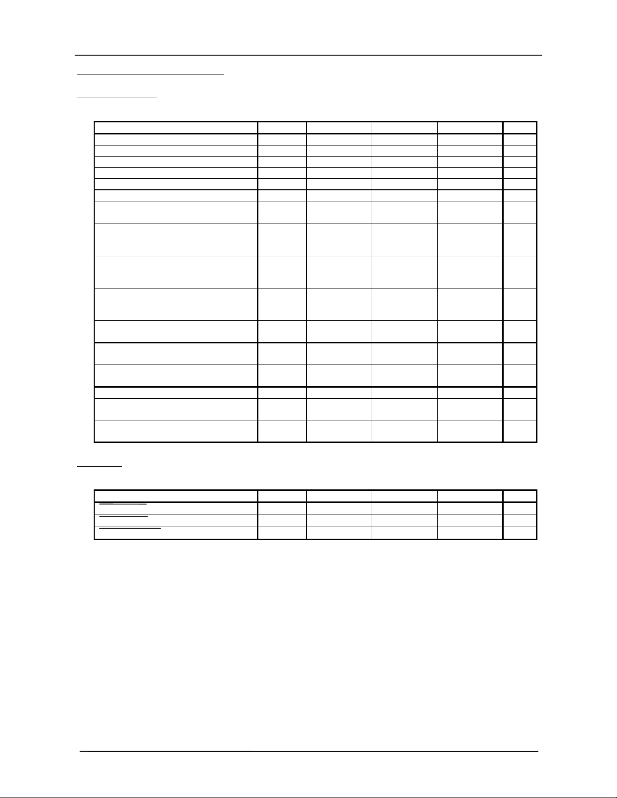
Pin No. Pin name I/O Function Classification
Digital Ground
Power supply
42,43 DVSS -
+5 V Digital power supply
44,45 DVDD -
47 WRQ I
48 CS I
49 JX I
53 SI I
55 SCLK I
56 CTRL0 I
57 DSP RESET I
Microcomputer interface Write Request pin
Microcomputer
interface
Microcomputer interface chip selector input pin (Pulldown)
Also used for SO control in addition to chip selection.
When only one AK7714 is used and SO is not used, CS="L" may be used
unchanged. SO and RDY will be Hi-z when CS ="H".
External condition jump pin (Pulldown) Program control
Microcomputer interface serial data input pin (Pulldown)
Microcomputer
interface
Microcomputer interface serial data clock input pin
Clock output control pin (Pulldown)
Control
Use of CTRL0 and CTRL1 allows the CLKO output and LRCLK/BITCLK
outputs
in the master mode to be fixed to “L” or “H”. See Function Description.
CTRL1 CTRL0 CLKO LRCLK BITCLK
0 0 Output Output Output
1 0 “L” Output Output
1 1 “L” “H”(“L”) “L”
Reset pin
Reset
Normally, DSP RESET and CODEC RESET are simultaneously controlled fo
use.
58 CODEC RESET I
Reset pin (for initialization)
59 INIT RESET I
M0018-E-00 ‘98/07
Used to input “L” to initialize the AK7714 at power-on.
- 7 -
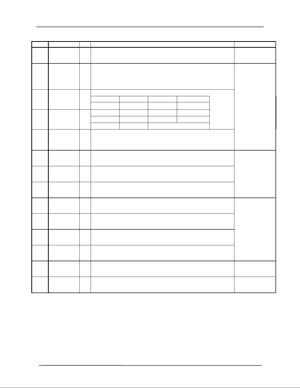
[ASAHI KASEI]
[AK7714]
Pin No. Pin name I/O Function Classification
Test pin: Leave open. Test
61 TESTOUT O
62 CTRL1 I
63 CKS0 I
64 CKS1 I
65 SMODE I
66,67 DVSS -
68 DVDD -
70,71 DVB -
73 AOUTR2 O
Clock output control pin (Pulldown)
Use of CTRL0 and CTRL1 allows the CLKO output and LRCLK/BITCLK
outputs
in the master mode to be fixed to “L” or “H”.
See CTRL0 ( pin 56 ) & Function Description.
Clock selector pin
CKS1 CKS0 XTI DSP
0 0 384fs 384fs
0 1 512fs 512fs
1 0 256fs 256fa
1 1 Test mode (disabled)
Slave/master mode selector pin
Set LRCLK and BITCLK to input or output mode.
SMODE="L": Slave mode (LRCLK and BITCLK are set to input mode.)
SMODE="H": Master mode (LRCLK and BITCLK are set to output mode.)
Digital ground
Power supply pin for digital section 5 V (typ)
+5 V Digital power supply
+5 V Power supply (normally analog) (Silicon substrate potential)
DAC2 Rch analog output pin
Control
Power supply
Analog section
74 AOUTL2 O
77 AOUTR1 O
78 AOUTL1 O
80 AVB -
82 VRDAL I
DAC2 Lch analog output pin
DAC1 Rch analog output pin
DAC1 Lch analog output pin
+5 V power supply (Silicon substrate potential) Power supply
DAC Reference voltage input pin
Analog section
Normally, connect to AVSS (pin 83).
M0018-E-00 ‘98/07
- 8 -
[ASAHI KASEI]
[AK7714]
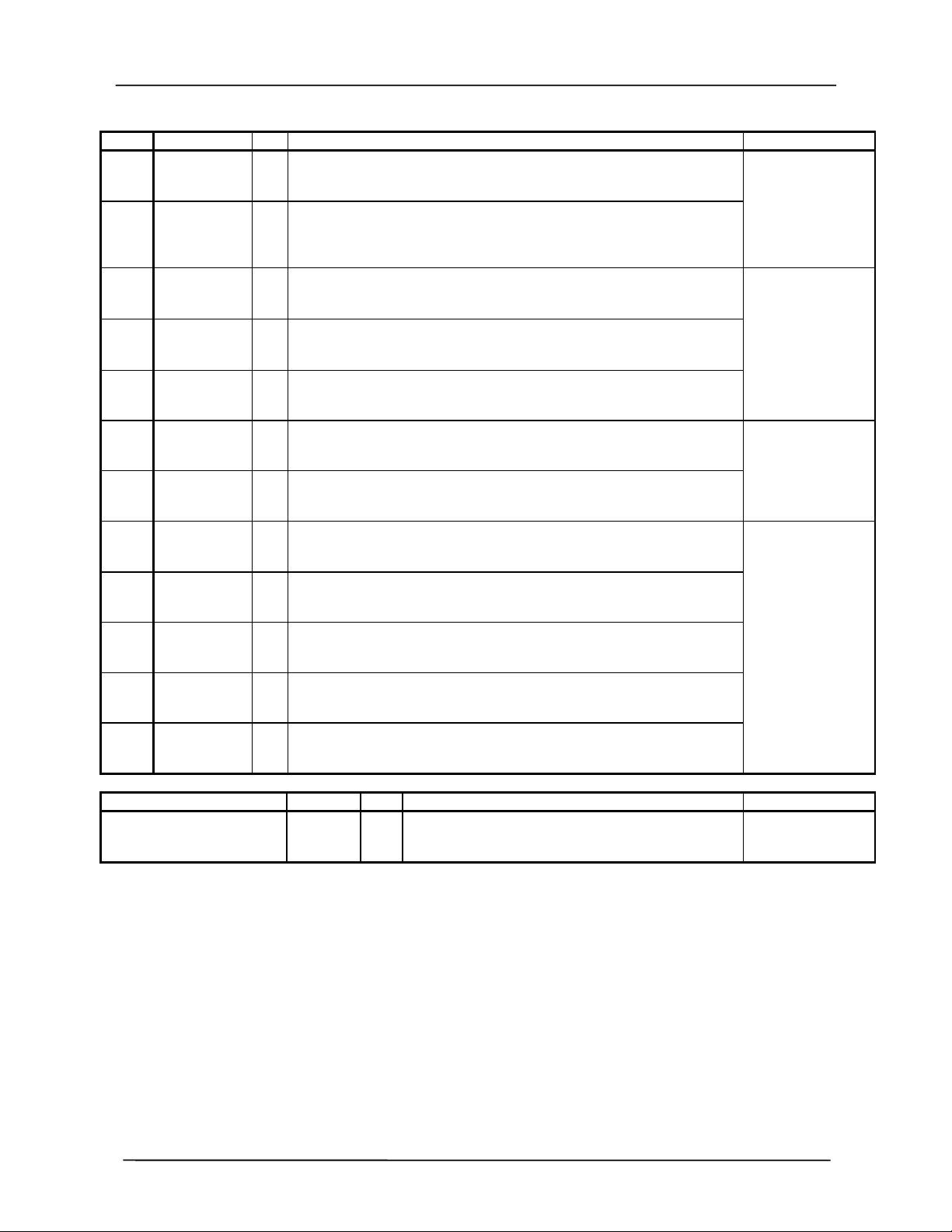
Pin No. Pin name I/O Function Classification
Power supply
83 AVSS -
84,85 AVDD -
Analog ground 0V
Power supply pin for analog section 5 V (typ) (Silicon substrate
potential)
+5 V Analog power supply
86 VRDAH I
87,88 VCOM O
89 VRADL I
90 AVSS -
91,92 AVDD -
93 VRADH I
95 AINR- I
96 AINR+ I
98 AINL- I
DAC Reference voltage input pin
µ
Normally, connect to AVDD (pin 84,85), and connect 0.1
capacitors between this and VRDAL.
Common voltage pin for analog section
µ
Connect 0.1
Do not use for the external circuit.
ADC Reference voltage input pin
Normally, connect to AVSS (pin 90).
Analog Ground 0V
+5 V Analog Power supply (Silicon substrate potential)
ADC Reference voltage input pin
Normally, connect to AVDD (pin 91,92), and connect 0.1
between this and VRADL.
ADC Rch analog inverted input pin
ADC Rch analog non-inverted input pin
ADC Lch analog inverted input pin
F and 10 µF capacitors between this and AVSS.
F and 10 µF
µ
F and 10 µF capacitors
Analog section
Power supply
Analog section
ADC Lch analog non-inverted input pin
99 AINL+ I
Pin No. Pin name I/O Function Classification
1,2,8,13,16,19,22,25,26,29,38
46,50,51,52,54,60,69,72,75,76
79,81,94,97,100
M0018-E-00 ‘98/07
NC -
NC ( No connection )
These pins should be left floating.
- 9 -
NC
[ASAHI KASEI]
Absolute maximum rating
(AVSS, DVSS = 0 V: All voltages indicated are relative to the ground.)
Item Symbol Min Max Unit
Power supply voltage
Analog (AVDD), Boards (DVB and AVB)
Digital (DVDD) (Note 1)
Input current (except for power supply pin ) IIN -10 +10 mA
Analog input voltage
AINL+, AINL-, AINR+, AINR-,
VRADH, VRADL, VRDAH, VRDAL
Digital input voltage (Note 1) VIND -0.3 VA+0.3 V
Operating ambient temperature Ta -40 85
Storage temperature Tstg -65 150
Note: 1. Must not exceed the maximum rating of 6.0 V (namely, VD ≤ (VA+0.3 V) ≤ 6.0 V).
WARNING: Operation at or beyond these limits may result in permanent damage of the device.
Normal operations are not guaranteed under these critical conditions in principle.
VA
VD
VINA
(VA is a power supply to supply silicon substrate potential.)
-0.3
-0.3
-0.3 VA+0.3
6.0
6.0 or (VA+0.3)
[AK7714]
V
V
V
°
C
°
C
Recommended operating conditions
(AVSS, DVSS = 0 V: All voltages indicated are relative to the ground.)
Items Symbol Min Typ Max Unit
Power supply voltage
Board (AVB, DVB), AVDD
DVDD
Reference voltage (VREF)
VRADH, VRDAH
VRADL, VRDAL
Note: 1. Start up VA simultaneously with or earlier than VD, and stop VD simultaneously with or earlier than VA.
2. When starting and stopping the power supply, meet the absolute maximum rating condition: VD ≤ (VA+0.3 V).
It is generally recommended to use at VD ≤ VA. However, the VD must be 4.75 volts or more.
3. The analog input voltage and output voltage are proportional to the VRADH and VRDAH voltages.
VA
VD
VRH
VRL
4.75
4.75
5.0
5.0
VA
0.0
5.25
VA
V
V
V
V
M0018-E-00 ‘98/07
- 10 -
[ASAHI KASEI]
(1) Analog characteristics
(Unless otherwise specified, Ta = 25°C; AVDD, DVDD, AVB, DVB = 5.0 V; VRADH = AVDD, VRADL = AVSS,
VRDAH = AVDD, VRDAL = AVSS; fs = 44.1 kHz; BITCLK = 64 fs ; XTI = 256 fs;
Signal frequency 1 kHz; measuring frequency = 10 Hz to 20 kHz; 20 bits; DSP section in the reset state; ADC
with all ifferential inputs )
ADC
section
DAC
section
Resolution 20 Bits
Dynamic characteristics
S/(N+D) (-0.5 dB) (Note 1) 86 92 dB
Dynamic range (A filter ) (Note 2) 94 99 dB
S/N (A filter ) 94 99 dB
Inter-channel isolation (f =1 kHz) 90 105 dB
DC accuracy
Inter-channel gain mismatching 0.1 0.3 dB
Gain drift 50
Analog input
Input voltage (Note 3)
Input impedance 220
Resolution 20 Bits
Dynamic characteristics
S/(N+D) (0 dB) 83 89 dB
Dynamic range (-60 dB) (A filter) (Note 2) 93 98 dB
S/N (A filter) 93 98 dB
Inter-channel isolation (f = 1 kHz) (Note 4) 90 105 dB
DC accuracy
Inter-channel gain mismatching (Note 4) 0.2 0.5 dB
Gain drift 50
Analog output
Output voltage (Note 5) 2.70 2.95 3.20 Vp-p
Load resistance 5
[AK7714]
Electric characteristics
Parameter Min Typ Max Unit
ppm/°C
±
1.9
±
2.0
±
2.1
Vp-p
Ω
k
ppm/°C
Ω
k
Note: 1. Single end input will result in poorer characteristics.
2. Indicates S/(N+D) when -60 dB signal is input.
3. The full scale for analog input voltage (∆AIN = (AIN+) - (AIN-)) can be represented By
(±FS = ±(VRADH-VRADL) × 0.4).
4. Specified for L and R of each DAC.
5. The full-scale voltage (0 dB) and output voltage are proportional to VRDAH voltage.
Analog output voltage (Typ. @ 0 dB) = 2.95 Vpp*VRDAH/5
M0018-E-00 ‘98/07
- 11 -
[ASAHI KASEI]
[AK7714]
(2) DC characteristics
(VDD = AVDD = DVDD = AVB = DVB = 5.0 V ±5%, Ta = 25°C)
Parameter Symbol Min Typ Max Unit
High level input voltage (Note 1)
Input pins other than XTI and test pins
XTI and test pins
Low level input voltage (Note 1)
Input pins other than XTI and test pins
XTI and test pins
High level output voltage Iout=-100µA
Low level output voltage Iout=100
Input leak current (Note 2)
Input leak current Pulldown pins (Note 3)
Note: 1. The test pins are as follows: TESTI1, TESTI2, TESTI3, TESTI4
2. The pulldown pins are not included.
3. The pulldown pins are as follows (Typ 50 kΩ):
TESTI1, TESTI2, TESTI3, TESTI4, SDINA, SDIND1, SDIND2, SDIN1, SDIN2, OPCL,
CS, JX, SI, CTRL0, CTRL1
Note: Regarding the input/output levels in the text, the low level is represented as "L" or 0, and the high level as "H" or 1.
In principle, "0" and "1" are used for the bus (serial/parallel), such as registers.
µ
A
VIH
VIL
VOH
VOL
Iin
Iid
2.4
70% VDD
VDD-0.5
-10
100
0.6
30% VDD
0.5
10
±
V
V
V
V
µ
A
µ
A
(3) Current consumption
(AVDD = AVB, DVB, DVDD = 5.0 V±5%, Ta = 25°C; master clock (XTI) = 22.5792MHz = 512 fs [fs = 44.1kHz]; when
operating for DAC 4 channel with 1 kHz sinusoidal wave full-scale input to each of ADC 2 ch analog input pins)
Power supply
Parameter Min Typ Max Unit
Power supply current
1) During operation
a) AVDD + AVB + DVB
b) DVDD (Note 1)
c) Total (a+b)
2) When INIT RESET= "L"(reference value)
Note 2
Power consumption
1) During operation
a) AVDD+AVB+DVB
b) DVDD (Note 1)
c) Total(a+b)
2) When INIT RESET ="L" (reference value)
Note 2
Note: 1. Varies slightly according to the frequency used and contents of the DSP program.
Note: 2. This is a reference value in case of using the crystal oscillator.
But, varies slightly according to the types of crystal oscillators.
41
87
128
7
205
435
640
35
162
850
mA
mA
mA
mA
mW
mW
mW
mW
M0018-E-00 ‘98/07
- 12 -

[ASAHI KASEI]
[AK7714]
(4) Digital filt er charact eri stics
Values described below are design values cited as references. These are not for guaranteeing the characteristics.
1) ADC Section:
(Ta = 25°C; AVDD, DVDD, AVB, DVB = 5.0 V ±5%; fs = 44.1 kHz)
Parameter Symbol Min Typ Max Unit
Pass band (-0.02 dB)
(-6.0 dB)
Stop band (Note 1) SB 24.35 kHz
Pass band ripple (Note 2) PR
Stop band attenuation (Notes 3,4) SA 80 dB
Group delay distortion
Group delay (Ts = 1/fs) GD 29.3 Ts
Note: 1. These frequencies scale with the sampling frequency (fs).
2. The pass band is from DC to 19.75 kHz when fs = 44.1 kHz.
3. The stop band is from 27.56 kHz to 2.795 MHz when fs = 44.1 kHz.
4. When fs = 44.1 kHz, the analog modulator samples analog input at 2.8224 MHz.
The input signal is not attenuate dBy the digital filter in the multiple bands (n x 2.8224 MHz ± 20.21 kHz ;
n = 0, 1, 2, 3...) of the sampling frequency.
PB 0
∆
GD
20.00
0
22.05
0.005 dB
±
0 µs
kHz
kHz
2) DAC section
(Ta = 25°C; AVDD, DVDD, AVB, DVB = 5.0 V ±5%; fs = 44.1 kHz)
Parameter Symbol Min Typ Max Unit
Digital filter
Pass band±0.07 dB (Note 1)
(-6.0 dB)
Stop band (Note 1) SB 24.1 kHz
Pass band ripple PR
Stop band attenuation SA 47 dB
Group delay (Ts = 1/fs ) (Note 2) GD - 15.3 Ts
Digital filter + Analog filter
Amplitude characteristics
0 to 20.0 kHz
Note: 1. The pass band and stop band frequencies are proportional to "fs" (system sampling rate), and are represente
PB = 0.4535 fs(@ -0.06 dB) and SB = 0.546 fs, respectively.
2. The caluculating delay time which occurred by digital filtering.
This time is from setting the 20-bit data of both channels on input register to the output of analog signal.
PB 0
- 22.05
0.5 dB
±
20.0
-
0.07 dB
±
kHz
kHz
M0018-E-00 ‘98/07
- 13 -
[ASAHI KASEI]
(5) Switching characteristi cs
1) System clock
(AVDD = AVB, DVB, DVDD = 5.0 V±5%, Ta = 25°C, CL = 20 pF)
Parameter Symbol Min Typ Max Unit
Master clock (XTI)
a) With a crystal oscillator:
256 fs: Frequency fMCLK 11.0 11.2896 12.288 MHz
384 fs: Frequency fMCLK 12.288 16.9344 18.432 MHz
512 fs: Frequency fMCLK 16.384 22.5792 22.5792 MHz
b)With an external clock input:
Duty factor (≤ 18.432 MHz)
( > 18.432MHz )
256 fs: Frequency
: High level width
: Low level width
384 fs: Frequency
: High level width
: Low level width
512 fs: Frequency
: High level width
: Low level width
Clock rise time
Clock fall time
LRCLK Sampling frequency fs 32 44.1
Slave mode: Clock rise time
Slave mode: Clock fall time
BITCLK fBCLK 48 64 fs
Slave mode: High level width
Slave mode: Low level width
Slave mode: Clock rise time
Slave mode: Clock fall time
fMCLK
tMCLKH
tMCLKL
fMCLK
tMCLKH
tMCLKL
fMCLK
tMCLKH
tMCLKL
tCR
tCF
tLR
tLF
tBCLKH
tBCLKL
tBR
tBF
40
45
11.0
30
30
12.288
20
20
16.384
17
17
100
100
50
50
11.2896 12.288 MHz
16.9344 18.432 MHz
22.5792 22.5792 MHz
1
60
55
6
6
48 kHz
10
10
6
6
[AK7714]
%
ns
ns
fs
ns
ns
ns
ns
2) Reset
(AVDD = AVB, DVB, DVDD = 5.0 V ±5%, Ta = 25°C, CL = 20 pF)
Parameter Symbol Min Typ Max Unit
INIT RESET (Note 1) tRST 150 ns
DSP RESET (Note 1) tRST 150 ns
CODEC RESET (Note 1) tRST 150 ns
Note 1. "L" is acceptable when power is turned on.
M0018-E-00 ‘98/07
- 14 -

[ASAHI KASEI]
[AK7714]
3) Audio interface
(AVDD = AVB, DVB, DVDD = 5.0 V ±5%,Ta = 25°C, CL = 20 pF)
Parameter Symbol Min Typ Max Unit
Slave mode
BITCLK frequency fBCLK 48 64 fs
BITCLK low level width tBCLKL 100 ns
BITCLK high level width tBCLKH 100 ns
Delay time from BITCLK"↑" to LRCLK
Delay time from LRCLK to BITCLK "↑"
Delay time from LRCLK to serial data output tLRD 70 ns
Delay time from BITCLK to serial data output tBSOD 70 ns
Serial data input latch hold time tBSIDS 40 ns
Serial data input latch setup time tBSIDH 40 ns
Master mode
BITCLK frequency fBCLK 64 fs
BITCLK duty factor 50
Delay time from BITCLK"↑" to LRCLK
Delay time from LRCLK to BITCLK"↑"
Delay time from LRCLK to serial data output tLRD 70 ns
Delay time from BITCLK to serial data output tBSOD 70 ns
Serial data input latch hold time tBSIDS 40 ns
Serial data input latch setup time tBSIDH 40 ns
tBLRD 40 ns
tLRBD 40 ns
tBLRD 40 ns
tLRBD 40 ns
M0018-E-00 ‘98/07
- 15 -
 Loading...