

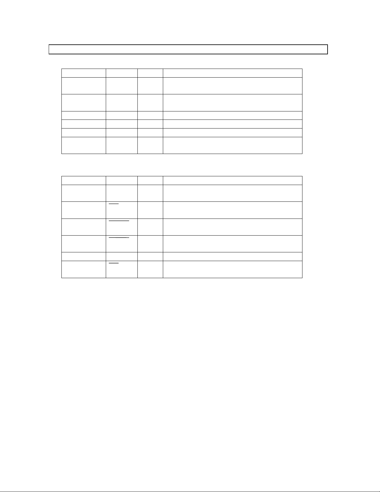
ASAHI KASEI [AK7712A-VT]
AK7712A-VT
Built-in 20-bit ADC/DAC Sophisticated Audio DSP
General Description
The AK7712A is a DSP(Digital Signal Processor) with built-in high performance 20bit 2ch ADC and 4ch DAC, on
purposeto control the sound field. It is possible to calculate 383 steps on 44.1kHz and 48kHz sampling respectively.
In case of 32kHz sampling, it can caluculate up to 511 steps. With a combination of this LSI and external memory
for delay data,it can berealized easily to control the sound field such as Echo, Surround Presence Controller, and
Key-control which are needed forsomething like Karaoke. Parametric Equalizing can be done without external
memory.
Features
[ DSP unit ]
Word length: 24-bit (data RAM)
Instruction cycle time: 54ns(maximum speed)
Multiplier: 24 × 16 → 40-bit
Divider: 16 ÷ 16 → 16-bit
Program RAM: 384 × 32 bit
External memory: DRAM,Pseudo-SRAM and SRAM can be connected (only use for delay data).
Sampling frequency: 32kHz∼48kHz
Automatic clear function of external RAM:
47msec after bringing RST high at fs=48kHz (include internal data RAM)
Microcomputer interface:
synchronized signal type 8-bit serial input 1 channel,
synchronized signal type 24-bit serial output 1 channel
Master clock: 512(511)/384(383)/256(255)fs
The value inside ( ) is maximum calculation steps.
512fs mode is available when 32kHz sampling is chosen.
Conversion of master/slave mode for LRCK and BCLK:
When master mode is selected, the outputs of LRCK and BCLK depend
on the set-up for input format.
Serial input ports(2~4ch), and output ports(2~6ch) : 16/20/24 bit words
[ ADC unit ]
20-bit 64 × Oversampling ∆Σ ADC: 2ch
S/(N+D): 92dB
DR, S/N: 98dB
[ DAC unit ]
20-bit 128 × Oversampling ∆Σ DAC: 4ch
S/(N+D): 86dB
DR, S/N: 97dB
Digital HPF (fc=1Hz)
[ Total ]
Power supply: +5V
Package: 100pin LQFP(0.5mm pitch)
0180-E-02 1997/12
- 1 -

ASAHI KASEI [AK7712A-VT]
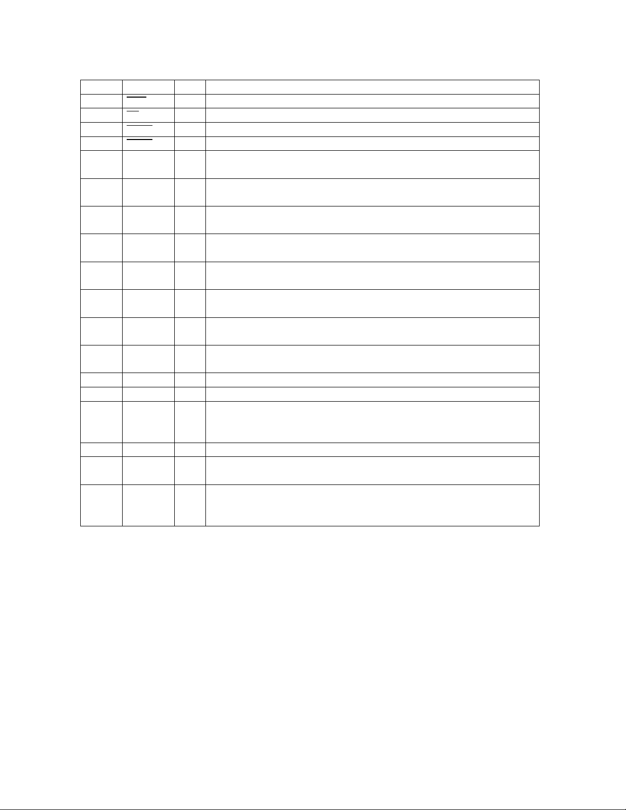
Detail Features
1) Calculate Unit
•
Multiplication: 24-bit × 16-bit→ 40-bit(fixed-point, 2 instruction cycle time)
•
Division: 16-bit ÷ 16-bit→ 16-bit(fixed-point, 17 instruction cycle time)
•
ALU: 34-bit arithmetic operation
24-bit arithmetic logic operation
•
Shift: 1-,2-,3-,4-,6-,8-,15-bit right/left shift
AK7712A has indirect shift function.
(A shift using DBUS data can not use DBUS
as multiplication input.)
•
Register: 34-bit × 4(ACC) [for ALU]
24-bit × 8(TMP) [for DBUS connection]
•
Double precision operation:
24-bit(data)×31-bit(coefficient), 45 × 31, 45 × 16
2) Internal Memory
•
Program RAM: 384 word × 32-bit
•
Data RAM: 128 word × 24-bit
•
Coefficient RAM: 256 word × 16-bit
•
Offset RAM: 40 word × 16-bit (for external memory access)
•
Microcomputer buffer: 16 word × 16-bit
3) External Memory Access (SRAM
•
Objective memory: 256k(32k × 8-bit),1M(128k × 8-bit) × 1 / SRAM
•
Pseudo-SRAM•DRAM)
256k(32k × 8-bit),1M(128k × 8-bit) × 1 / Pseudo-SRAM
256k(64k × 4-bit),1M(256k × 4-bit) × 2 or × 1 / DRAM
(Half volume of 1M DRAM is used as 512k memory.)
•
Treating bit length: 16-bit (24-bit is available, but double time is needed for access.)
•
The number of times to access:
SRAM, 256k Pseudo-SRAM ; 76 at 384fs
: DRAM, 1M Pseudo-SRAM ; 64 at 384fs (32 at one DRAM)
: SRAM, 256k Pseudo-SRAM ; 51 at 256fs
: DRAM, 1M Pseudo-SRAM ; 42 at 256fs (21 at one DRAM)
•
Memory access time:
less than 100nsec
•
Maximum address length:
65535 sampling times (at 1M SRAM)
2.048sec at 32kHz, 1.486sec at 44.1kHz, 1.365sec at 48kHz
4) Input/Output Port
•
Input: 2ch analog input: 20-bit ADC, DR=98dB (16-bit at BCLK=32fs)
[when built-in ADC is connected.]
2ch digital input: MSB justified 20-bit (16bit at BCLK=32fs)
…
MSB first serial input
[when built-in ADC is isolated.]
2ch digital input: MSB justified 16-
•
Output: 4ch analog output: 20-bit DAC, DR=97dB(16-bit at BCLK=32fs)
•
24-bit / LSB justified 16-•24-bit
…
MSB first serial input
[when built-in ADC is connected.]
4ch digital output: MSB justified 20-bit (16bit at BCLK=32fs)
…
MSB first serial output
[when built-in ADC is isolated.]
2ch digital output: MSB justified 16-
•
24-bit/ LSB justified 16-bit
…
MSB first serial output
5) Cascade connection with this LSI is possible.
6) Interface to Microcomputer:
synchronized 8-bit serial input / synchronized 24-bit serial output
7) Calculation Cycle: max 18.432MHz(54nsec) [at 48.0kHz, 384fs, 5V]
8) Master/Slave conversion of LRCK
BCLK is possible.
9) BCLK: 32fs/48fs/64fs (64fs only at master mode)
0180-E-02 1997/12
- 2 -

ASAHI KASEI [AK7712A-VT]
AK7712A Block Diagram
1) ADC,DAC Inside Connection Mode (OPCL: L)
AK7712A Block Diagram
Note: Please use SDIN2,SDDA and SDDA2 with "L" or open.
SDAD,SDOUT2 and SDOUT3 output "L".
0180-E-02 1997/12
- 3 -
ASAHI KASEI [AK7712A-VT]
2) ADC,DAC Outside Connection Mode (built-in ADC,DAC isolation mode) (OPCL:H)
0180-E-02 1997/12
- 4 -
ASAHI KASEI [AK7712A-VT]
AK7712A DSP unit Block Diagram
Data Address
CP0,1 DP0,1
CRAM
256 × 16
CBUS (16-bit)
DBUS (24-bit)
MPX16 MPX24
X Y
Multiply
16 × 24→40
40-bit
DRAM
128 × 24
24-bit
D0a7 AD0a16
Delay Data
16-bit
Micom I/F
Control
D
E
C
PRAM
384 × 32
PC
Stack:1Level
Ext RAM
Control
Interface
OFRAM
40 × 16
Microcomputer Serial
34-bit
MUL DBUS
SHIFT
34-bit
A B
ALU
34-bit
Overflow Margin:4bit
DR0a3
24-bit
Overflow Data
Generator
Division
16 ÷ 16→16
Peak Detector
TMP 8 × 24-bit
2 × 24/16-bit
2 × 20/16-bit
2 × 24/16-bit
2 × 20/16-bit
2 × 20/16-bi
note 1: Normally it's connected to built-in ADC
2: Normally it's connected to built-in DAC1
3: Normally it's connected to built-in DAC2
SDIN1 (24/16-bit)
MSB/LSB justified Serial In
SDIN2 (20/16-bit)
MSB justified Serial In (note 1)
SDOUT1 (24/16-bit)
MSB/LSB justified Serial Out
SDOUT2 (20/16-bit)
MSB justified Serial Out (note 2)
SDOUT3 (20/16-bit)
MSB justified Serial Out (note 3)
0180-E-02 1997/12
- 5 -
ASAHI KASEI [AK7712A-VT]
Ordering Guide
AK7712A-VT -40∼+85°C 100pin LQFP
AKD7712A Evaluation Board
Pin Layout
0180-E-02 1997/12
- 6 -
ASAHI KASEI [AK7712A-VT]
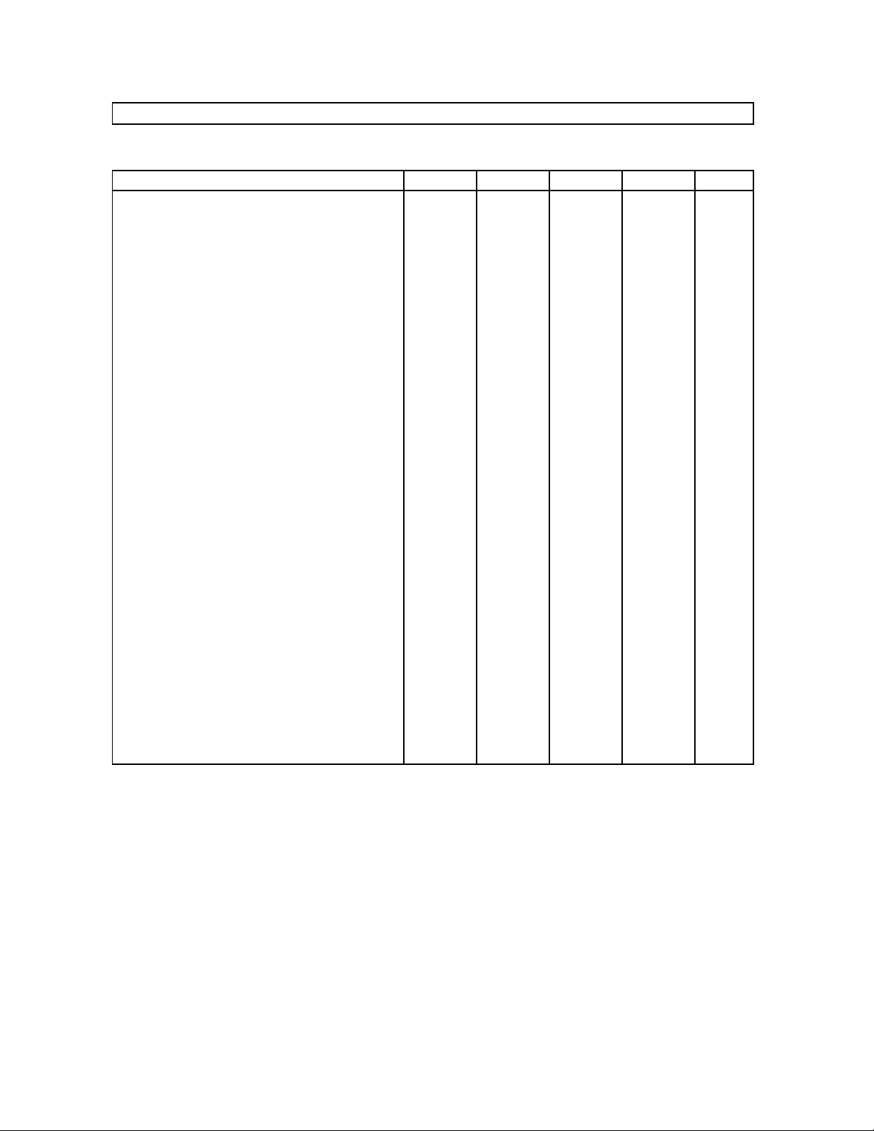
Pin / Function
Power Supply
Pin No. Pin name I/O Function
24, 32, 50,
70, 73
25, 31, 49,
69, 72
87, 97 AVDD - Analog power supply
86, 96 AVSS - Analog ground
79, 99 AVB - Analog substrate power supply
10, 11, 74,
75
External RAM Interface Signal
Pin No. Pin name I/O Function
41∼48,
51∼59
40 WE O Write signal output
39 RESCE O RAS for external DRAM
38 CASRF O CAS for external DRAM
61∼68 IO0∼IO7
60 OE O Output enable signal output
DVDD - Digital power supply
DVSS - Digital ground
DVB - Digital substrate power supply
A16∼A0
O Address output for external RAM
(A0:LSB justified, A16:MSB justified)
for external SRAM/ Pseudo-SRAM/ DRAM
/ Pseudo-SRAM-CE
/ Pseudo-SRAM refresh
I/O Data input/output for external RAM
for external SRAM/ Pseudo-SRAM/ DRAM
0180-E-02 1997/12
- 7 -

ASAHI KASEI [AK7712A-VT]
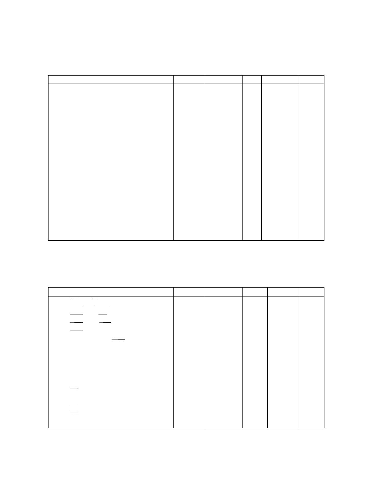
Microcomputer Interface Signal, Controls Signal, Input/Output Data, Reset, etc.
Pin No. Pin name I/O Function
30 WRQ I Command register reset input
for microcomputer interface
33 SCLK I Clock input for serial data input
for microcomputer interface
36 DRDY O Output data ready output
for microcomputer interface
34 SI I Serial data input
for microcomputer interface
37 SO O Serial data output
for microcomputer interface
(Hi-Z state at CS="H")
35 WRDY O Data write ready output
for microcomputer interface
(Hi-Z state at CS="H")
29 CS I Chip select input
for microcomputer interface
0180-E-02 1997/12
- 8 -
ASAHI KASEI [AK7712A-VT]
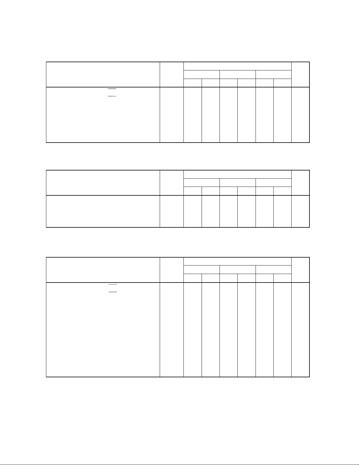
AK7712A Control Signal, Input/Output Data Signal, Reset, etc.
Pin No Pin name I/O Function
6 RST I Reset input ("L" Reset) (note 1)
5 PD I Power down (note 1)
3 PDAD I AD reset control (note 1)
4 PDDA I DA reset control (note 1)
19 SDIN1 I Serial data input 1
•
MSB justified 16-
24-bit / LSB justified 16-•24-bit
18 SDOUT1 O Serial data output 1
•
MSB justified 16-
24-bit / LSB justified 16-bit
12 SDIN2 I Serial data input 2 (OPCL : "H" ) (note 2)
•
MSB justified 16-
20-bi
13 SDAD O Serial data output 2 (OPCL : "H" ) (note 3)
•
MSB justified 16-
20-bit, common set-up with SDIN2
15 SDDA I Serial data input 3 (OPCL : "H" ) (note 2)
MSB justified 16-
•
20-bit, common set-up with SDOUT2
14 SDOUT2 O Serial data output 3 (OPCL : "H" ) (note 3)
•
MSB justified 16-
20-bit
16 SDDA2 I Serial data input 4 (OPCL : "H" ) (note 2)
MSB justified 20-bit (16-bit at BCLK=32fs )
17 SDOUT3 O Serial data output 4 (OPCL : "H") (note 3)
MSB justified 20-bit (16-bit at BCLK=32fs)
21 BCLK I/O Clock input/output for serial data input
22 LRCK I/O L/R channel identify signal input/output
Interface clock select
20 SMODE I
Input/output set-up for each clock pin of LRCK and BCLK
"L":slave mode(21,22 input), "H":master mode(output)
23 CLKO O Master clock output (note 4)
27 XTO O Output for quartz oscillator
When an external clock is input, this pin should be left floating.
26 XTI I Input for quartz oscillator
A crystal can be connected between this pin and XTO, or an external CMOS
clock can be input on this pin.
note:1 About the directions, please refer the paragraph of power down reset control on P.65.
2 Set to "L" or "open" when OPCL is "L".
3 The output is "L" when OPCL is "L".
4 During a timing of changing CONTROL REGISTER, CLKO is instability.
0180-E-02 1997/12
- 9 -
ASAHI KASEI [AK7712A-VT]
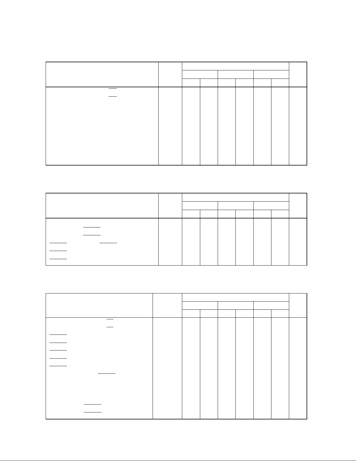
Analog Relational Pins
Pin No. Pin name I/O Function
93 AINL+ I ADC Lch analog non-inverted input
92 AINL- I ADC Lch analog inverted input
91 AINR+ I ADC Rch analog non-inverted input
90 AINR- I ADC Rch analog inverted input
84 AOUTL1 O DAC1 Lch analog output 1
83 AOUTR1 O DAC1 Rch analog output 1
81 AOUTL2 O DAC2 Lch analog output 2
80 AOUTR2 O DAC2 Rch analog output 2
85 VRDAL I Standard voltage input of DAC unit
(normally connected to analog ground)
88 VRDAH I Standard voltage input of DAC unit
(normally connected to 87 pin.
0.1u and 10uF capacitor are connected
between this pin and VRDAL pin.)
95 VRADL I Standard voltage input of ADC unit
(normally connected to analog ground)
98 VRADH I Standard voltage input of ADC unit
(normally connected to 97 pin.
0.1u and 10uF capacitor are connected
between this pin and VRADL pin.)
94 VCOM O Common voltage
(0.1u and 10uF capacitor are connected
between this pin and analog ground.)
0180-E-02 1997/12
- 10 -
ASAHI KASEI [AK7712A-VT]
Test Pin, etc.
Pin No. Pin name I/O Function
77 DZF1 O Zero input find (for DAC1)
76 DZF2 O Zero input find (for DAC2)
1 TSTI1 I Test input 1 ; use as "L" or open
28 TSTI2 I "L": CLKO(23pin) output
"H": CLKO(23pin)→"L"
7 TSTIO1 I/O Test input 1 ; use as "L" or open
8 TSTIO2 I/O Test input 2 ; use as "L" or open
9 TSTIO3 I/O Test input 3 ; use as "L" or open
2 OPCL I ADC,DAC connection choice
"L": connect , "H": separate
71 DZFSET I Zero point find set
"H": DZF output , "L": DZF output→"L"
78, 82,
89, 100
NC - NC pins do not be bonded inside.
0180-E-02 1997/12
- 11 -
ASAHI KASEI [AK7712A-VT]
Absolute Maximum Ratings
(AVSS,DVSS=0V; note 1)
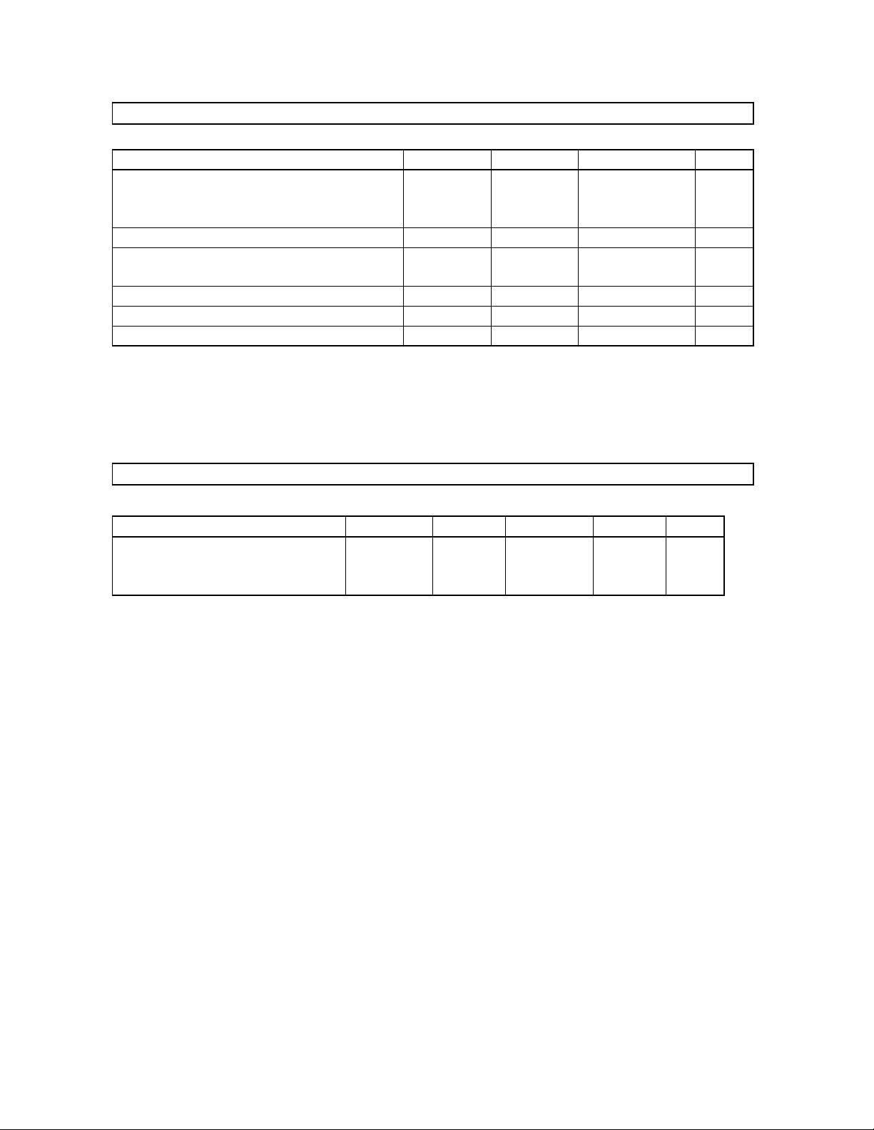
Parameter Symbol min max Unit
DC Power supply: analog power
digital power(DVDD) (note 2)
substrate power(AVB,DVB)
Input current (except power supply) IIN Analog input voltage
AINL+,AINL-,AINR+,AINR-,VREF
Digital input voltage (note 2) VIND -0.3 (VB)+0.3 V
Ambient temperature Ta -40 85
Storage temperature Tstg -65 150
note 1: All the value mean the voltage against the ground pin.
2: Maximum absolute value must be within 6.0V, i.e. VB+0.3V ≤ 6.0V.
Warning: To operate beyond these limits may result in permanent damage to the device.
Normal operation is not guaranteed at these extremes.
VA
VD
VB
VINA
-0.3
-0.3
-0.3
-0.3 (VA)+0.3 V
6.0
(VB)+0.3
6.0
10
±
mA
°
°
V
V
V
C
C
Recommended Operating Conditions
(AVSS,DVSS=0V; note 1)
Parameter Symbol min typ max Unit
Power supply: analog power
digital power (DVDD)
substrate power (AVB,DVB)
(note 2,3,4)
note 1: All the value mean the voltage against the ground pin.
2: The VA and VB should be powered at the same time or earlier than VD.
3: The VA and VB are connected together through the chip substrate and has several ohms resistors.
The VA and VB should be supplied from the same power unit.
4: Analog input/output voltages are proportional to the voltages of VRADH,VRDAH.
* AKM assumes no responsibility for the usage beyond the conditions in this data sheet.
VA
VD
VB
4.75
4.75
4.75
5.0
5.0
5.0
5.25
VB
5.25
V
V
V
0180-E-02 1997/12
- 12 -
ASAHI KASEI [AK7712A-VT]
Analog Characteristics
(Ta=25°C; AVDD,DVDD,AVB,DVB=5.0V; VRADH=AVDD,VRADL=AVSS,VRDAH=AVDD,VRDAL=AVSS;
fs=44.1kHz; BCLK=64fs master mode; MCLK=256fs; input signal frequency=1kHz; 20-bit;
measurement band width=10Hz∼20kHz; DSP unit is reset; ADC differential input; unless otherwise specified.)
Parameter min typ max Units
ADC unit :
Resolution 20 Bits
Dynamic characteristics
S/(N+D) ( -0.5dB ) 86 92 dB
S/N (A-Weight) 94 98 dB
Dynamic range (A-Weight) (note 1) 94 98 dB
Interchannel isolation (f=1kHz) 90 105 dB
DC Accuracy
Interchannel gain mismatch 0.1 0.3 dB
Gain drift - 50 Analog input
1.9
Input voltage (note 2)
Input impedance 220
DAC unit :
Resolution 20 Bits
Dynamic characteristics
S/(N+D) ( 0 dB ) 80 86 dB
S/N (A-Weight) 93 97 dB
Dynamic range (A-Weight) (note 1) 93 97 dB
Interchannel isolation (f=1kHz) (note 4) 90 105 dB
DC Accuracy
Interchannel gain mismatch (note 4) 0.2 0.5 dB
Gain drift - 50 Analog output
Output voltage (note 3) 2.65 2.90 3.15 Vp-p
Load resistance 5
note 1: S/(N+D) with an input signal of -60dB below full-scale.
2: The full-scale of analog input voltage(AIN = (AIN+) - (AIN-) ) equals to
FS = ±(VRADH - VRADL) × 0.4
±
3: The full-scale of output voltage(0dB) is proportional to VRDAH.
Aout(typ. @0dB) = 2.9Vpp × VRDAH/5
4: Between L channel and R channel of each DAC.
±
2.0
±
2.1
±
ppm/°C
Vp-p
k
Ω
ppm/°C
k
Ω
0180-E-02 1997/12
- 13 -
ASAHI KASEI [AK7712A-VT]
Digital Filter Characteristics
This data is not the guaranteed characteristic value but the designed value as a reference.
ADC unit :
(Ta=25°C; VA,VD,VB=5.0V±5%; fs=44.1kHz)
Parameter Symbol min typ max Units
Passband (±0.06dB)
( -6.0 dB) (note 1)
Stopband (note 1) SB 24.35 kHz
Passband ripple (note 2) PR
Stopband attenuation (note 3,4) SR 80 dB
Group delay distortion
Group delay (Ts=1/fs) GD 29.3 Ts
note 1: The frequencies of passband/stopband are proportional to the sampling frequency (fs).
2: Passband is DC to 19.75kHz at fs=44.1kHz.
3: Stopband is 27.56kHz to 2.795MHz at fs=44.1kHz.
4: The analog modulator samples the input at 2.8224MHz for fs=44.1kHz. There is no rejection of
input signals at those band width which are multiples of the sampling frequency(n x 2.8224MHz
±20.21kHz; n=0,1,2,3…).
PB 0
GD
∆
20.00
0
22.05
0.005 dB
±
0us
kHz
kHz
DAC unit :
(Ta=25°C; VA,VD,VB=5.0V±5%; fs=44.1kHz;)
Parameter Symbol min typ max Units
Digital filter
Passband ( -0.2 dB) (note 1)
( -6.0 dB)
Stopband (note 1) SB 24.3 kHz
Passband ripple PR
Stopband attenuation SA 41 dB
Group delay (Ts = 1/fs) (note 2) GD - 14.7 - Ts
Digital filter + analog filter
Amplitude characteristics
0∼20kHz
note 1: The frequencies of passband/stopband are proportional to the sampling frequency (fs);
PB=0.4535fs(@-0.2dB), SB=0.546fs(@-41dB).
2: The calculating delay time is occurred by digital filtering. This is the time from the setting
20-bit data on input register to the output of analog signal. (at fs=44.1kHz)
PB 0
- 22.05
-
0.5 - dB
±
20.0
-
0.05 dB
±
kHz
kHz
0180-E-02 1997/12
- 14 -
ASAHI KASEI [AK7712A-VT]
DC Characteristics
(AVDD=DVDD; AVD,DVB=5.0V±5%; Ta=25°C)
Parameter Symbol min typ max Units
High level input voltage
Low lev e l input voltage
VIH
VIL
70%VDD
-
-
-
-
30%VDD
V
V
High level input voltage
Iout=-20uA
Low lev e l input voltage
Iout= 20uA
Input leak current (note 1)
Input leak current (note 2)
(pull-down pin)
note 1: except pull-up/pull-down pin
2: Pull-down pin(Typ 50kΩ) is as follows; PDAD, PDDA,SDIN2,SDDA,SDDA2,TSTI1,TSTI2,
TSTO1,TSTO2,TSTO3,OPCL pin.
(Ta=25°C; AVDD,DVDD,AVB,DVB=5.0V; Master clock = 18.432MHz, XTI=384fs [fs=48kHz]; Input 1kHz full scale
sine wave input from 2ch analog input pin of ADC and output to 4ch DAC.)
Power supply
Parameter min typ max Units
Power supply current
Normal operation (RST=PD="H")
AVDD + AVB + DVB
DVDD
Power-down mode (RST=PD="L")
AVDD + AVB + DVB+ DVDD (note 3)
VOH
VOL
Iin
Iid
VDD-0.1
-
-
-
47
51
20
-
-
-
100
70
80
250
0.1
±
-
10
-
V
V
uA
uA
mA
mA
uA
Power dissipation
Normal operation
Power-down mode
note 3: This is the value in the conditions that external clock(XTI,BCLK,LRCK) is "L", SCLK is "H".
0180-E-02 1997/12
- 15 -
490
0.1
750
1.25
mW
mW
ASAHI KASEI [AK7712A-VT]
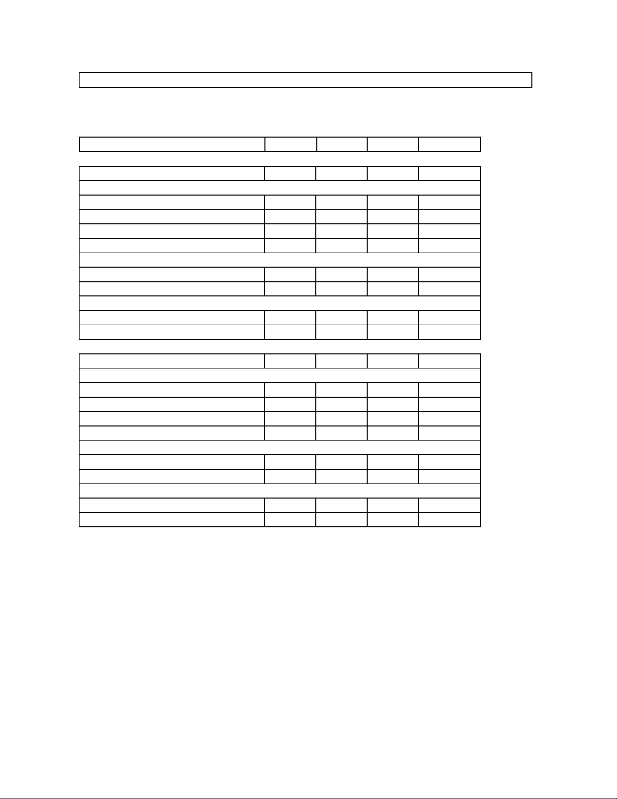
Switching Characteristics
••••
Clock
(Ta=25°C; VA,VD,VB=5.0V±5%; C
=20pF)
L
Parameter Symbol min typ max Units
Control clock frequency
Master clock
Quartz oscillator mode
256fs:
384fs:
512fs:
f
CLK
f
CLK
f
CLK
8.192
12.288
12.288
11.2896
16.9344
16.384
12.288
18.432
18.432
MHz
MHz
MHz
External clock mode
Duty cycle
256fs:
Pulse width Low
Pulse width High
384fs:
Pulse width Low
Pulse width High
512fs:
Pulse width Low
Pulse width High
Audio serial data clock (BCLK)
Channel select clock (LRCK)
Duty cycle
Microcomputer serial data clock (SCLK
Pulse width Low
Pulse width High
f
t
t
f
t
t
f
t
t
f
f
f
t
t
CLK
CLKL
CLKH
CLK
CLKL
CLKH
CLK
CLKL
CLKH
BLK
S
SLK
SLKL
SLKH
40
8.192
30
30
12.288
20
20
12.288
20
20
1.024
32
49
30
30
50
11.2986
16.9344
16.384
2.8224
44.1
50
60
12.288
18.432
18.432
3.072
48
51
12.288
%
MHz
ns
ns
MHz
ns
ns
MHz
ns
ns
MHz
kHz
%
MHz
ns
ns
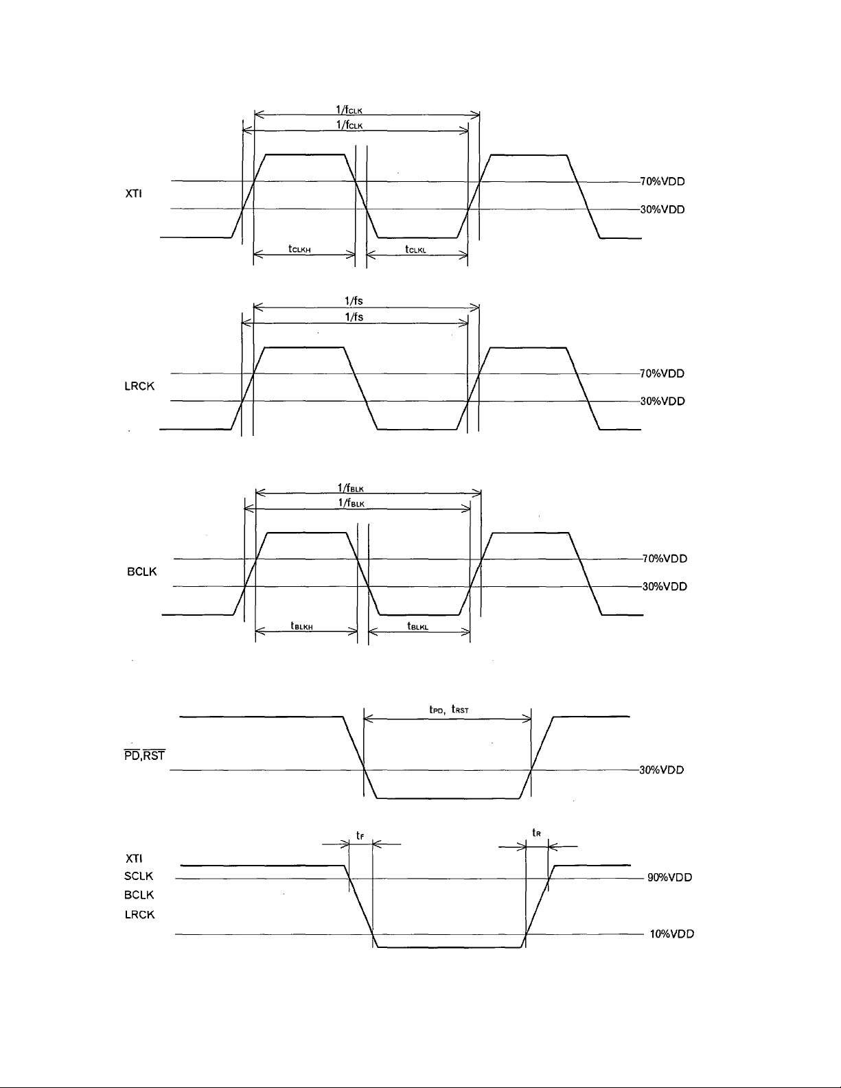
Reset timing
PD pulse width
RST pulse width
t
PD
t
RST
100
100
ns
ns
Clock falling time
[XTI, BICK, LRCK, SCLK] (note)
Clock rising time
[XTI, BICK, LRCK, SCLK] (note)
t
f
10
t
r
10
ns
ns
note : At input of external CMOS clock for XTI.
0180-E-02 1997/12
- 16 -
ASAHI KASEI [AK7712A-VT]
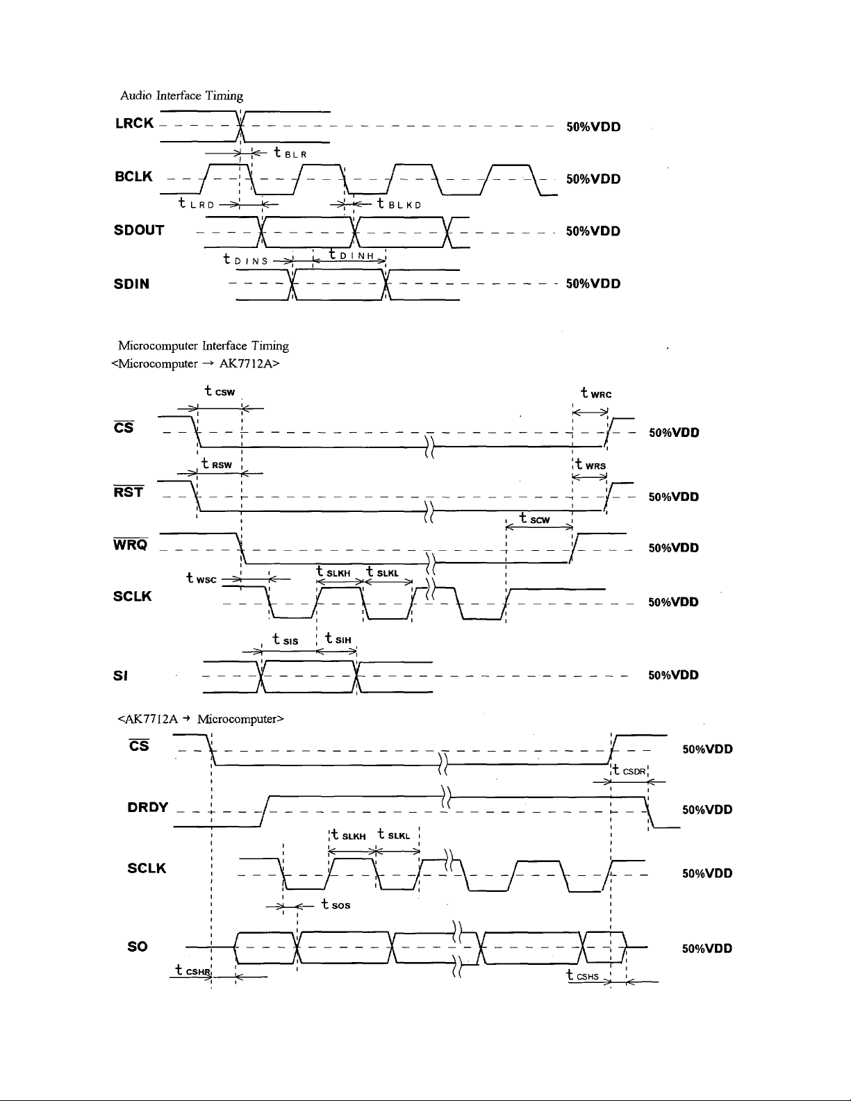
1) Audio Interface Timing
(AVDD=DVDD,AVB,DVB=5.0V±5%,Ta=25°C;
Master clock 16.9344MHz,XTI=384fs[fs=44.1kHz]; CL=20pF)
Parameter Symbol min typ max Units
Slave mode
BCLK cycle
BCLK pulse width Low
pulse width High
Time from BCLK"↓" to LRCK (note 1)
Delay time from LRCK to DOUT(MSB)
Delay time from BCLK"↓" to DOUT
Latch hold time of SDIN
Latch setup time of SDIN
t
t
t
t
t
t
t
t
BLK
BLKL
BLKH
BLR
LRD
BLKD
DINH
DINS
312.5
100.0
100.0
30-t
40
40
BLKH
30+t
70
70
BLKL
ns
ns
ns
ns
ns
ns
ns
ns
Master mode
BCLK cycle
Duty cycle
BCLK pulse width Low
pulse width High
Time from BCLK"↓" to LRCK
Delay time from LRCK to DOUT(MSB)
Delay time from BCLK"↓" to DOUT
Latch hold time of SDIN
Latch set Up time of SDIN
t
t
t
t
t
t
t
t
BLK
BLKL
BLKH
BLR
LRD
BLKD
DINH
DINS
100.0
100.0
-20
40
40
64fs
50
20
70
70
ns
ns
ns
ns
ns
ns
ns
ns
ns
note 1 : This standard value is provided for not to be overlapped the edge of LRCK and BCLK"↑" each other.
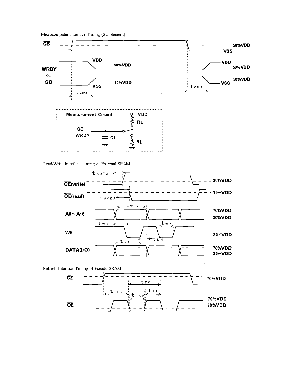
2) Microcomputer Interface Timing
(AVDD=DVDD,AVB,DVB=5.0V±5%,Ta=25°C;
master clock 16.9344MHz,XTI=384fs[fs=44.1kHz];CL=20pF)
Parameter Symbol min typ max Units
From CS"↓" to WRQ"↓"
From RST"↓" to WRQ"↓"
From WRQ"↑" to CS"↑"
From WRQ"↑" to RST"↑"
From WRQ"↓" to SCLK"↓"
From Last SCLK"↑" to WRQ"↑"
SCLK cycle
SCLK pulse width Low
pulse width High
SI latch hold time
SI latch set Up time
From CS"↓" to
t
t
t
t
t
t
t
t
t
t
t
t
CSW
RSW
WRC
WRS
WSC
SCW
SLK
SLKL
SLKH
SIH
SIS
CSHR
166(note1)
cancellation of SO,WRDY "Hi-z" (note2)
From CS"↑" to SO,WRDY"Hi-z" (note2)
From CS"↑" to DRDY"↓"
From SCLK"↓" to SO setup time (note2)
t
t
t
CSHS
CSDR
SOS
note 1 : Master clock cycle × 3
note 2 : See timing chart.
100
100
100
100
100
200
80
80
50
50
100
800
100
40
ns
ns
ns
ns
ns
ns
ns
ns
ns
ns
ns
ns
ns
ns
ns
0180-E-02 1997/12
- 17 -
ASAHI KASEI [AK7712A-VT]
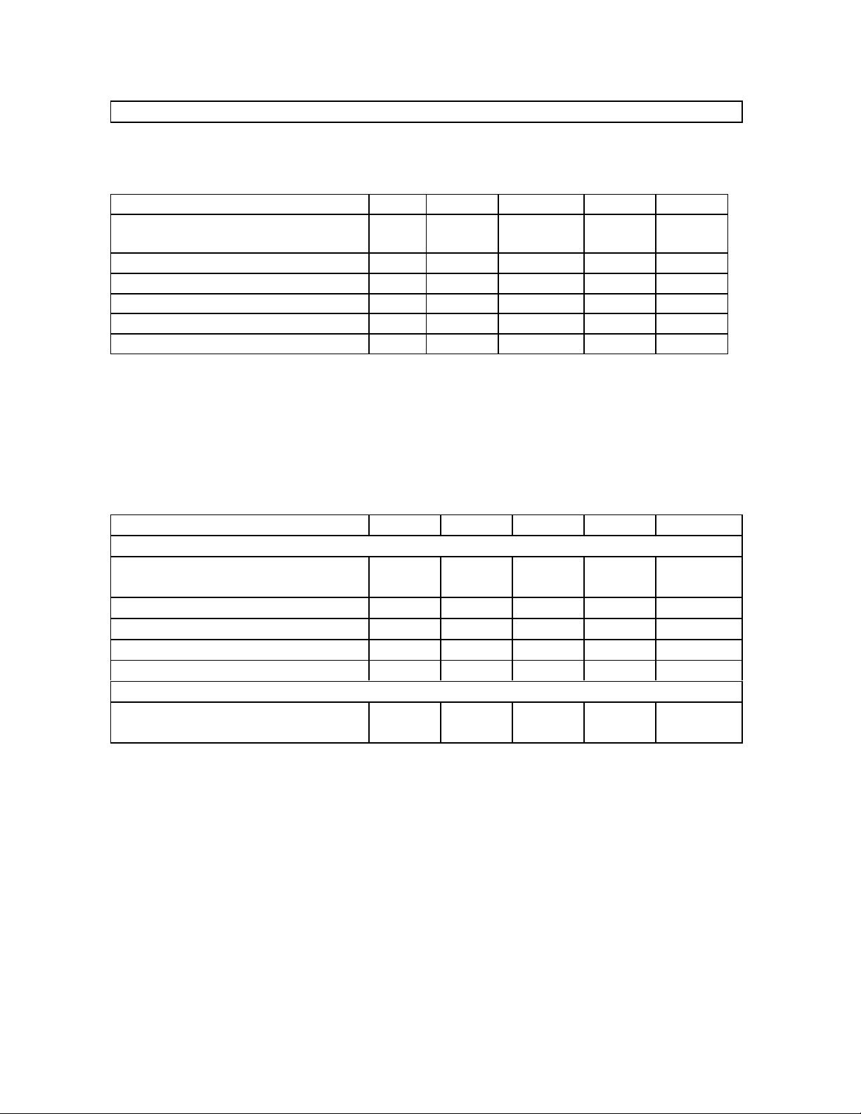
3)Read/Write Interface Timing of External RAM
(AVDD,DVDD,AVB,DVB=5.0V±5%, Ta=25°C, CL=20pF)
XTI(MHz)
18.432 16.934 12.288Parameter Symbol
Units
min max min max min max
Address delay time from OE "↑" (writing)
Address delay time from OE "↓" (reading)
Access time
Address set-up time
Data set time
Data hold time
Pulse width to write
t
t
t
t
t
t
t
AOEW
AOER
WCY
WD
DS
DH
WP
-15
105
10
80
10
60
1570-18
115
12
90
12
70
1880-20
170
15
135
15
90
20
110nsns
ns
ns
ns
ns
ns
4) Refresh Interface Timing of Pseudo SRAM(External RAM)
(AVDD,DVDD,AVB,DVB=5.0V±5%, Ta=25°C, CL=20pF)
XTI(MHz)
18.432 16.934 12.288Parameter Symbol
Units
min max min max min max
Auto refresh cycle
Pulse width of refresh command
Delay time of refresh command
Pre-charge time of refresh
t
FC
t
FAP
t
RFD
t
FP
145
80
100
35
162
90
110
40
210
135
160
60
ns
ns
ns
ns
5) Read/Write Interface Timing of Pseudo SRAM(External RAM) (Static Column Mode)
(AVDD,DVDD,AVB,DVB=5.0V±5%, Ta=25°C, CL=20pF)
XTI(MHz)
18 .432 16.934 12.288Parameter Symbol
min max min max min max
Address delay time from OE "↑" (writing)
Address delay time from OE "↑" (reading)
Column address hold time
SC mode read/write cycle
Address setup time
Pulse width of chip enable
Column address hold time (after write)
Chip enable time
Column address setup time
Pulse width of write command
Data set time
Data hold time
t
t
t
t
t
t
t
t
t
t
t
t
AOEW
AOER
CAH
RSC
AS
CE
AHW
CW
ASW
WP
DW
DH
-15
110
80
10
180
10
95
10
35
50
10
1570-18
1880-20
120
90
12
200
12
105
12
40
60
12
170
135
15
280
15
140
15
60
90
15
Units
20
110nsns
ns
ns
ns
ns
ns
ns
ns
ns
ns
ns
0180-E-02 1997/12
- 18 -
ASAHI KASEI [AK7712A-VT]
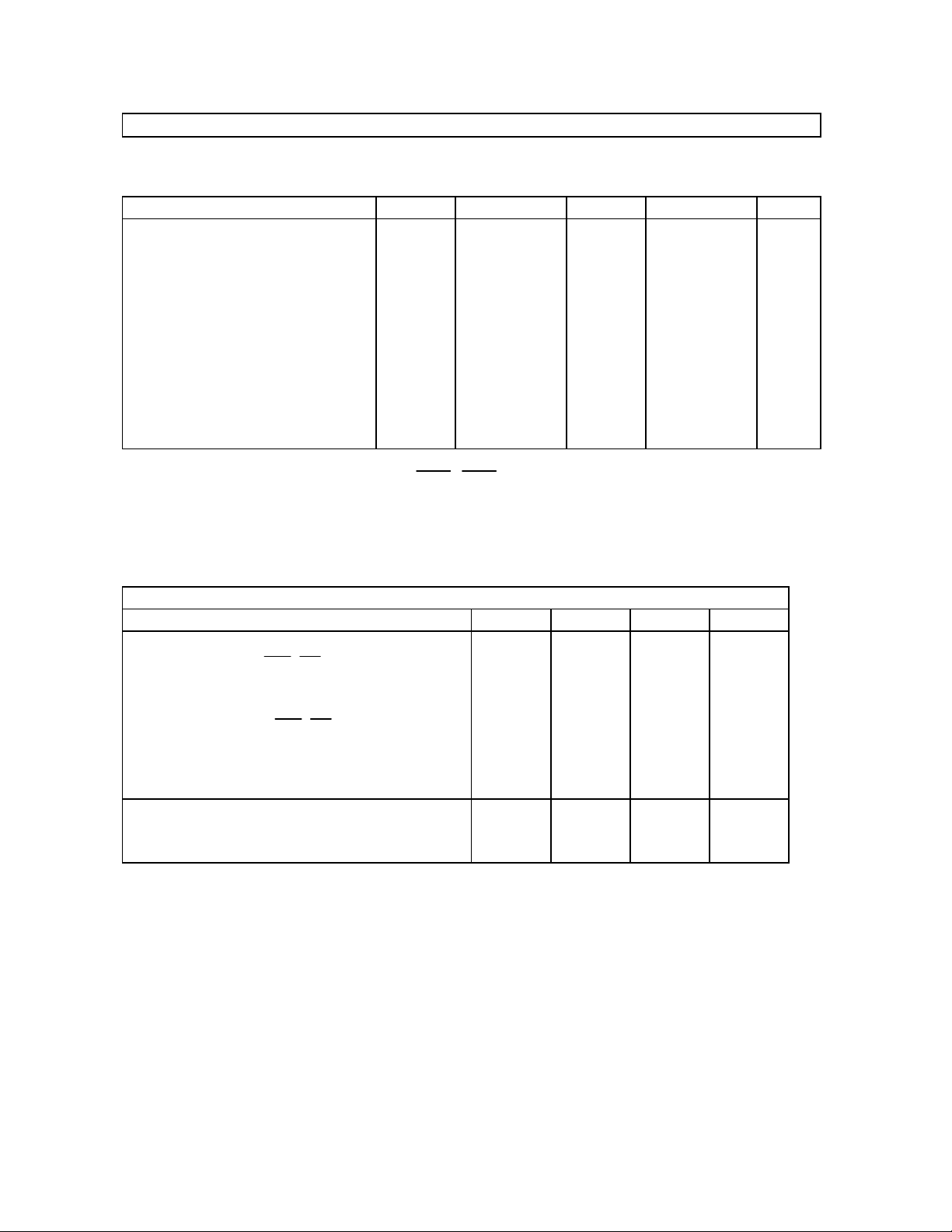
6) Read/write Interface Timing of Pseudo SRAM(External RAM) (normal mode)
(AVDD,DVDD,AVB,DVB=5.0V±5%, Ta=25°C, CL=20pF)
XTI(MHz)
18.432 16.934 12.288Parameter Symbol
Units
min max min max min max
Address delay time from OE "↑" (writing)
Address delay time from OE "↑" (reading)
Hold time of column address
Address setup time
Pulse width of chip enable
Pre-charge time of chip enable
Chip enable time
Pulse width of write command
Data set time
Data hold time
t
t
t
t
t
t
t
t
t
t
AOEW
AOER
CAH
AS
CE
P
CW
WP
DW
DH
-15
110
10
90
40
90
35
100
10
1570-18
120
12
100
50
100
40
110
12
1880-20
170
15
135
60
135
60
160
15
20
110nsns
ns
ns
ns
ns
ns
ns
ns
ns
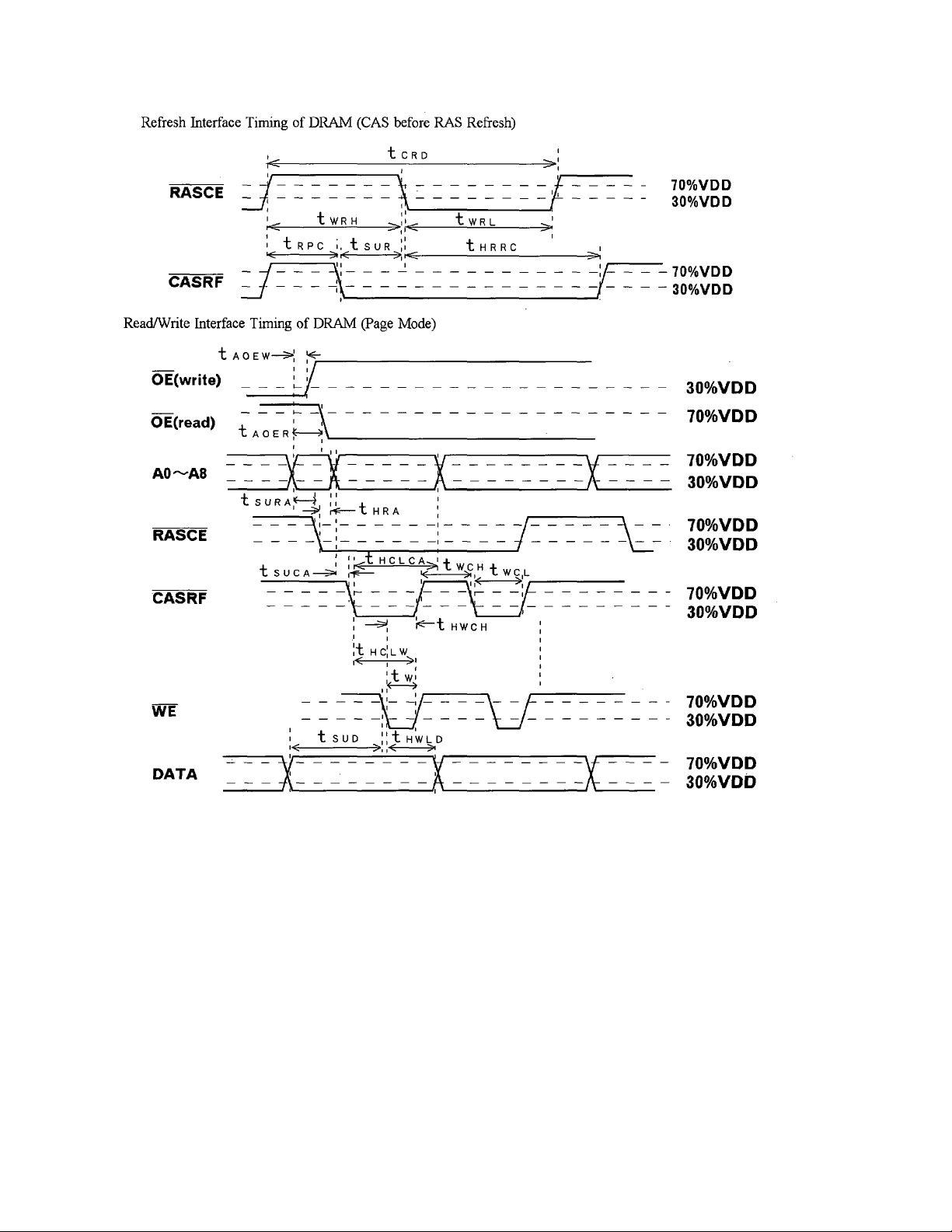
7) Refresh Interface Timing of DRAM(External RAM) (CAS before RAS Refresh)
(AVDD,DVDD,AVB,DVB=5.0V±5%, Ta=25°C, CL=20pF)
18.432 16.934 12.288Parameter Symbol
min max min max min max
Read cycle
Pulse width of RASCE"H"
Pulse width of RASCE"L"
•
RASCE Pre-charge
CASRF hold time
CASRF setup time at auto refresh
CASRF hold time at auto refresh
t
t
t
t
t
t
CRD
WRH
WRL
RPC
SUR
HRRC
240
105
105
80
10
200
8) Read/Write Interface Timing of DRAM(External RAM) (Page Mode)
(AVDD,DVDD,AVB,DVB=5.0V±5%, Ta=25°C, CL=20pF)
18.432 16.934 12.288Parameter Symbol
min max min max min max
Address delay time fromOE "↑" (write)
Address delay time fromOE "↓" (read)
RASCE preceded address setup time
RASCE followed address hold time
CASRF preceded address setup time
CASRF followed address hold time
CASRF hold time after write
Write hold time after CASRF
Write pulse width
Data setup time
Data hold time after write
Pulse width of CASRF"H"
Pulse width of CASRF"L"
t
AOEW
t
AOER
t
SURA
t
HRA
t
SUCA
t
HCLCA
t
HWCH
t
HCLW
t
W
t
SUD
t
HWLD
t
WCH
t
WCL
-15
10
12
10
45
40
55
40
0
60
22
54
1570-18
XTI(MHz)
260
120
120
90
12
220
XTI(MHz)
12
14
12
45
43
65
43
0
70
24
62
1880-20
360
170
170
130
15
320
15
18
15
60
60
90
60
100
32
90
0
Units
ns
ns
ns
ns
ns
ns
Units
20
110nsns
ns
ns
ns
ns
ns
ns
ns
ns
ns
ns
ns
0180-E-02 1997/12
- 19 -
ASAHI KASEI [AK7712A-VT]
Timing Waveform
0180-E-02 1997/12
- 20 -
ASAHI KASEI [AK7712A-VT]
0180-E-02 1997/12
- 21 -
ASAHI KASEI [AK7712A-VT]
0180-E-02 1997/12
- 22 -
ASAHI KASEI [AK7712A-VT]
Read/Write Interface Timing of Pseudo SRAM (Static Column Mode)
0180-E-02 1997/12
- 23 -
ASAHI KASEI [AK7712A-VT]
0180-E-02 1997/12
- 24 -
ASAHI KASEI [AK7712A-VT]
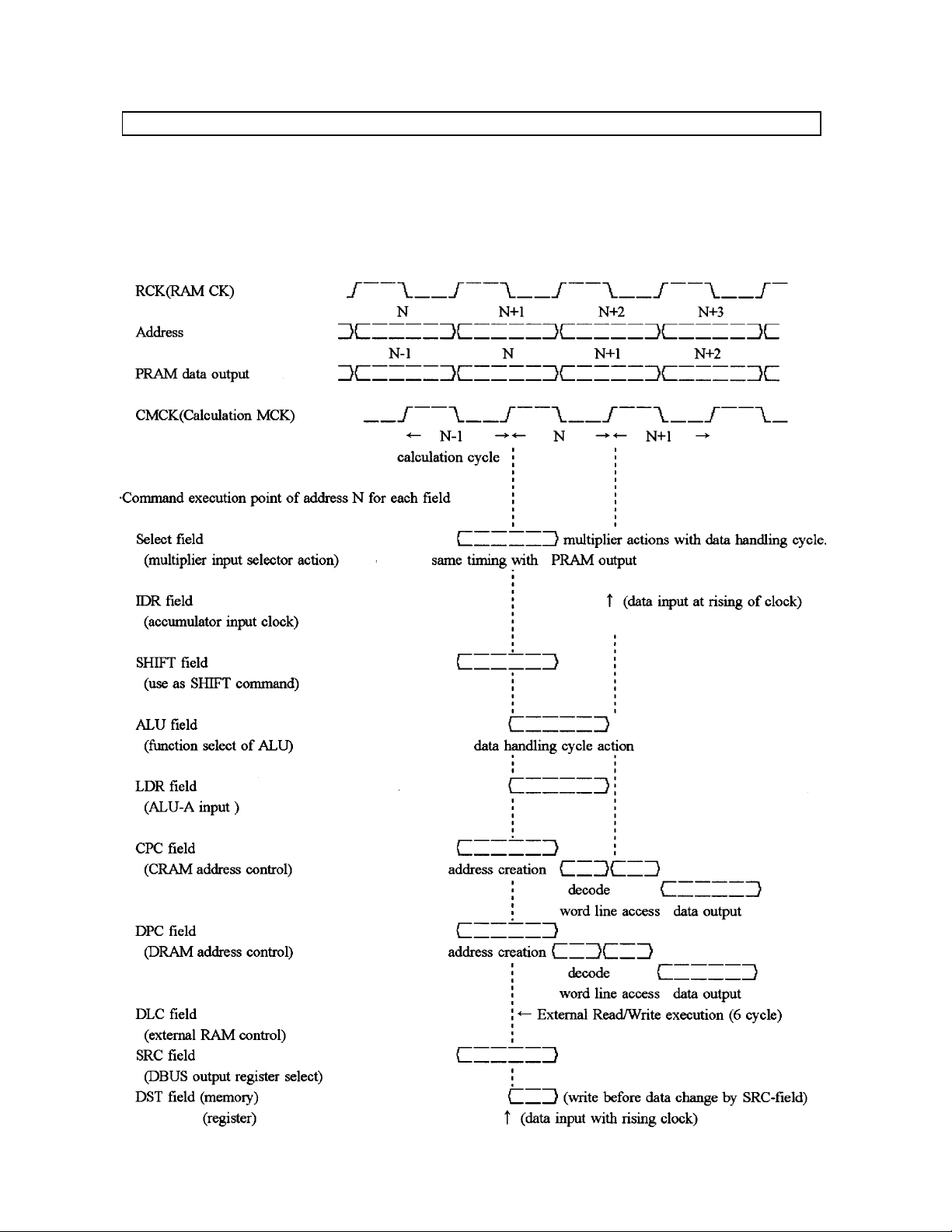
Function Manual
DSP unit : Execution Timing of Each Command
Each Blocks(PRAM,DRAM,CRAM,Calculation unit,etc.) actions on pipeline. On controlling of this pipeline, each
stages(command fetch, command decode and execution) are handled in parallel, The operations for each block is
executed by 32-bit holizontal code. Therefore each operations are executed equivalently in one machine cycle. The
following is the executing timing of each command.
0180-E-02 1997/12
- 25 -
ASAHI KASEI [AK7712A-VT]
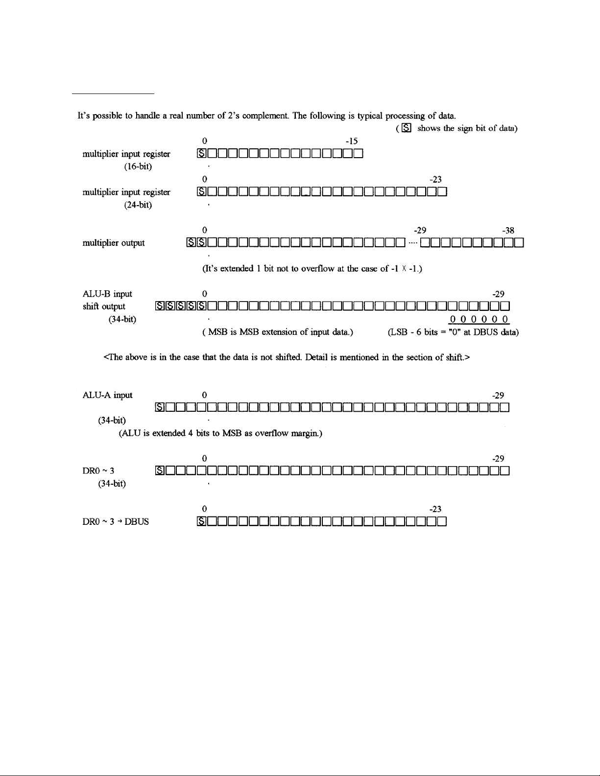
Calculation Function
1) Arithmetic System
0180-E-02 1997/12
- 26 -
ASAHI KASEI [AK7712A-VT]
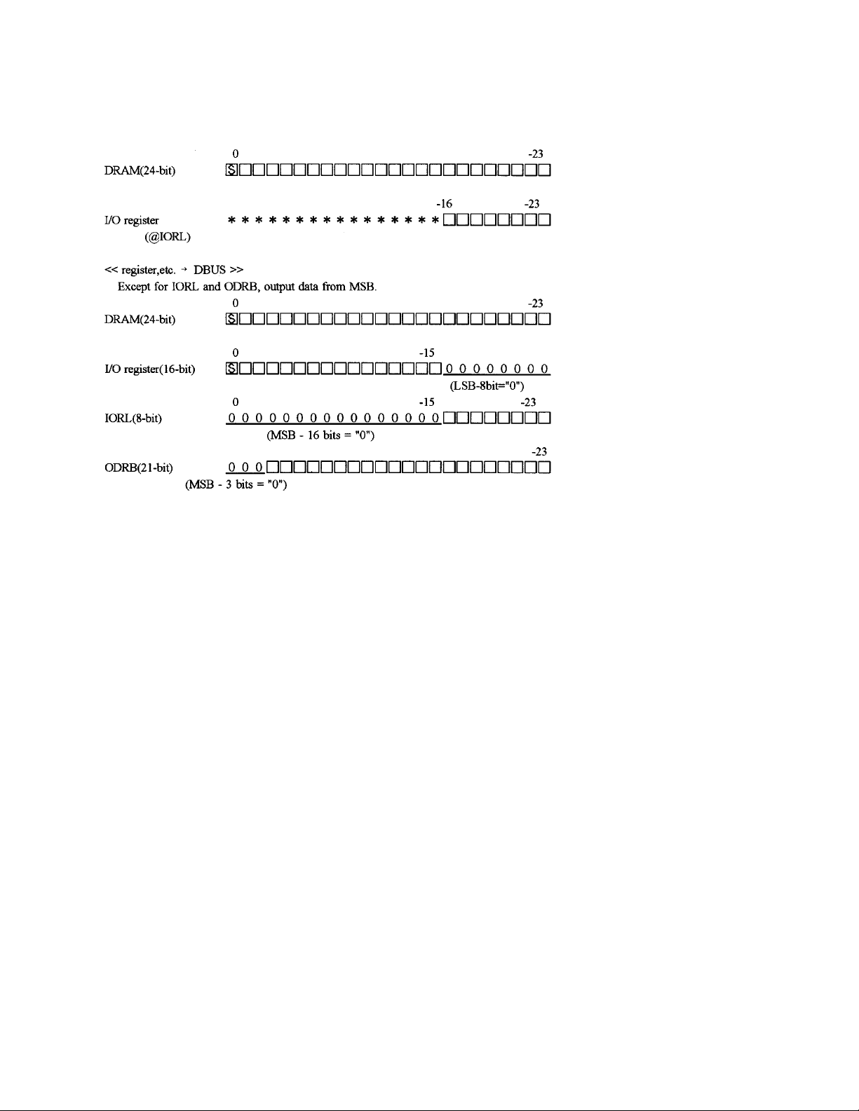
<< DBUS → register,etc. >>
Except for @IORL, take data from MSB.
0180-E-02 1997/12
- 27 -
 Loading...