

AKM AK6480AM, AK6480AF, AK6440AM, AK6440AF, AK6420AM Datasheet
...
ASAHI KASEI [AK6420A/40A/80A]
AK6420A / 40A / 80A
2K / 4K / 8Kbit Serial CMOS EEPROM
Features
ADVANCED CMOS EEPROM TECHNOLOGY
Wide Vcc (1.8V ∼ 5.5V) operation
AK6420A
AK6440A
AK6480A
ONE CHIP MICROCOMPUTER INTERFACE
• •
2048 bits: 128 × 16 organization
• •
4096 bits: 256 × 16 organization
• •
8192 bits: 512 × 16 organization
- Interface with one chip microcomputer's serial communication port directly
LOW POWER CONSUMPTION
- 0.75mA Max (Read operation)
- 0.8
A Max (Standby mode)
µ
HIGH RELIABILITY
-Endurance : 100K cycles
-Data Retention : 10 years
SPECIAL FEATURES
- High speed operation ( f
MAX
- Automatic write cycle time-out with auto-ERASE
- Automatic address increment (READ)
- Ready/Busy status signal
- Software and Hardware controlled write protection
IDEAL FOR LOW DENSITY DATA STORAGE
- Low cost, space saving, 8-pin package (SOP, SSOP)
=1MHz: Vcc=2.5V )
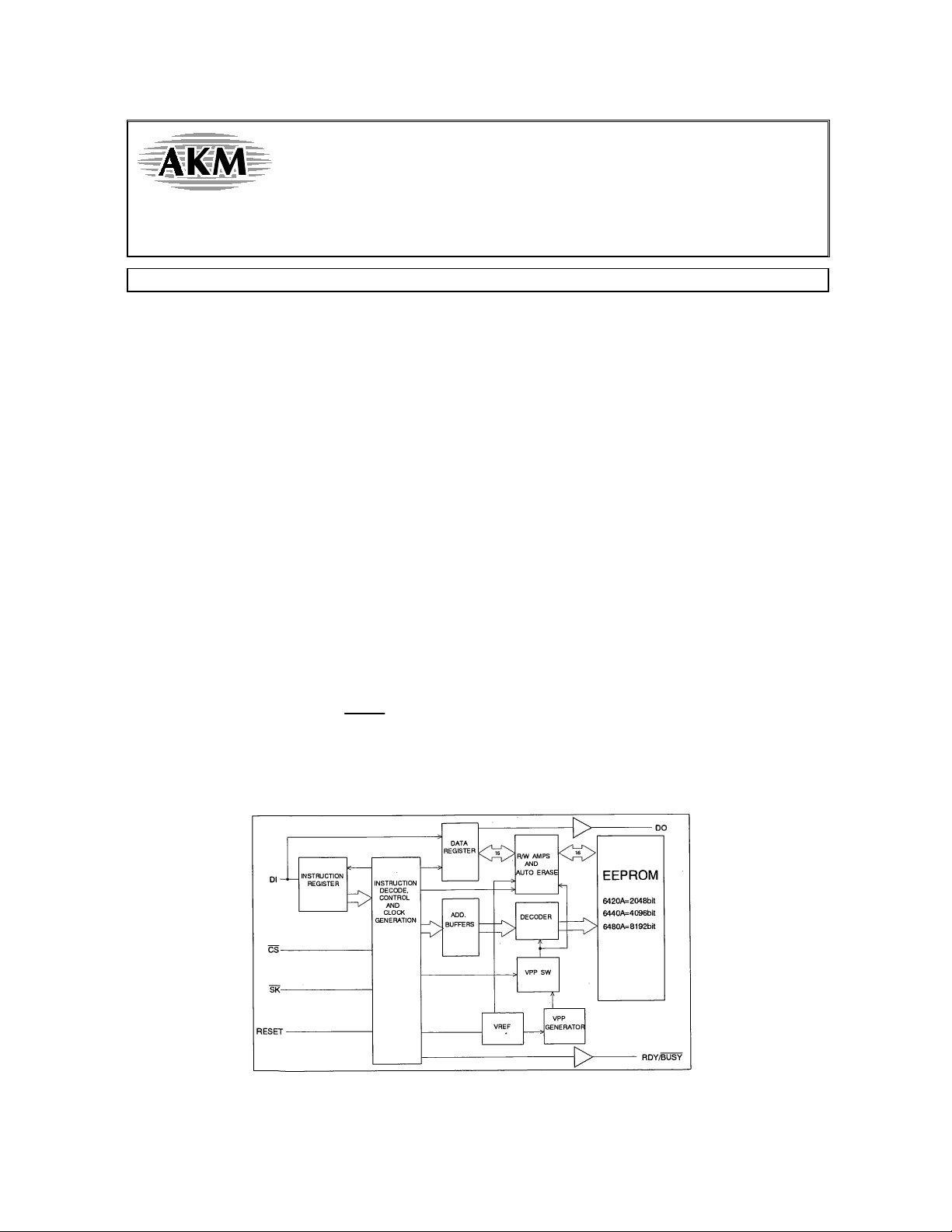
Block diagram
DAS01E-00 1999/05
- 1 -
ASAHI KASEI [AK6420A/40A/80A]
General Description
The AK6420A/40A/80A is a 2048/4096 /8192bit, serial, read/write, n on-v olatile memory de vice fabricated using an
advanced CMOS EEPR OM technolog y. The AK6420A has 2048bits of memory organized into 128 registers of 16
bits each. The AK6440A has 4096bits of memory organized into 256 registers of 16 bits each. The AK6480A h as
8192bits of memory organized into 512 registers o f 16 bits each. The AK6420A/40A/80A can oper ate f ull function
under wide operating v oltage range f rom 1.8V t o 5.5V. The charge up circui t is integ r ated f or high v oltage gene ra tion
that is used f or write oper ation.
The AK6420A/40A/80A can connect to the serial comm unication port of popular one chip mi crocomputer dir ectly ( 3
line negative clock synchronous interf ace). At write operation, AK6420A/40A/80A takes in the write data f rom data
input pin (DI) to a regi ster synchronou sly with rising edge of input pul se of serial clo ck pin (SK). And at read operation,
AK6420A/40A/80A takes out the read data from a register to data output pin (DO) synchronousl y with falling edge of
SK.
The AK6420A/40A/80A has 4 instructions such as READ, WRITE, WREN (write enab le) and WRDS (write disable).
Each instruction is organized b y op-code b loc k (8bits), address b lo c k (8bits) a nd data (8bi ts × 2). When input lev el of
SK pin is high le vel and input level of chip select (CS) pin is ch anged from hi gh level to low level, AK6420A/40A/80A
can receive the instructions .
Special features of the AK64 20A/40A/80A incl ude : automatic write time-out with auto-ERASE, Ready/Busy status
signal output and ultr a-low standb y po wer mode wh en deselected (CS=high).
•
Software and Hardw are co ntrolled w rite protection
The AK6420A/40A/80A has 2 (hardwa re and softw are) write prote ction function s.
After power on o r after execution of WRDS (write disab le) instruction, execution of WRITE instructi on will be disab led.
This write protection condition continue s until WREN instruction is ex e cuted or V cc is remov ed from the pa rt.
Execution of READ i nstruction is in dependent of both WREN and WRDS instructions.
Reset pin should be low le v el when WRITE instruction is executed. When the Reset pin is high level, the WR ITE
instruction is not ex e cuted.
•
Ready/Busy status signal
During the automatic write time-out pe riod (BUSY statu s), the AK6420A/40A/80A can 't ac cept the othe r instructions .
The AK6420A/40A/80A has 2 function s to kno w the Busy status f rom e x terior.
The RDY/BUSY pin indicates the Busy status regardless of the CS pin statu s. The RDY/BUSY pin outputs the low
level regardless of the CS pin status during Busy status. Except the above status, this pin outputs high level.
Also the DO pin indicates the Busy statu s. When input le vel of SK pin i s low level and input le v el of CS pin is changed
from high lev el to lo w l e v el, the AK6420A/40A/80A i s in t he statu s output mode and the DO pi n indicates the
Ready/Busy status. The Ready/Busy status outputs on DO pin u ntil CS pin i s changed f rom low level to high le v el, o r
first bit ("1") of op- code of next instruction is giv en to t he part. E xcept w hen the d e vice is i n the status outpu t mode or
outputs data, the DO pin i s in the high impedan ce state .
Ty pe of Products
Model Memory size Temp.Range Vcc Package
AK6420AF
AK6420AM
AK6440AF
AK6440AM
AK6480AF
AK6480AM
2Kbits
4Kbits
8Kbits
-40°C∼85°C
-40°C∼85°C
-40°C∼85°C
-40°C∼85°C
-40°C∼85°C
-40°C∼85°C
1.8V ∼ 5.5V
1.8V ∼ 5.5V
1.8V ∼ 5.5V
1.8V ∼ 5.5V
1.8V ∼ 5.5V
1.8V ∼ 5.5V
8pin Plastic SOP
8pin Plastic SSOP
8pin Plastic SOP
8pin Plastic SSOP
8pin Plastic SOP
8pin Plastic SSOP
DAS01E-00 1999/05
- 2 -
ASAHI KASEI [AK6420A/40A/80A]
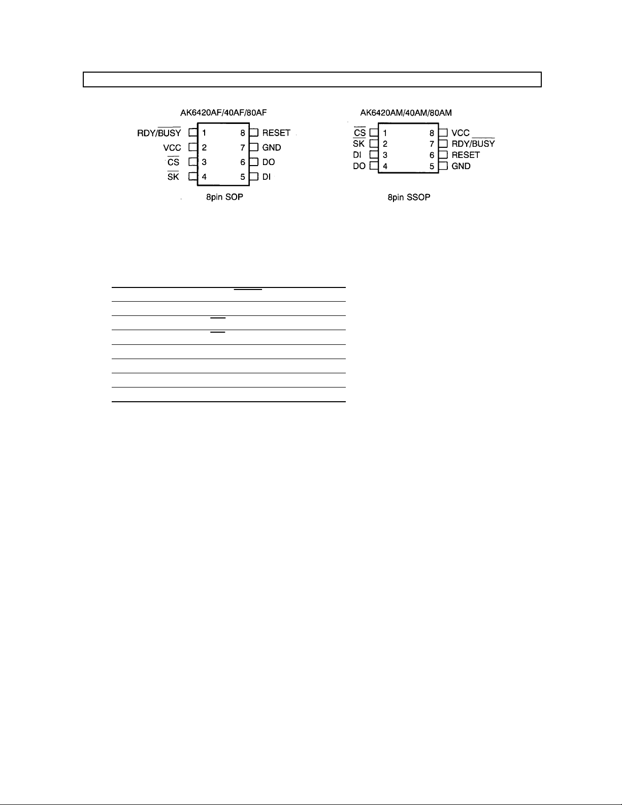
Pin arrangement
Pin Function
Pin No. Pin name I/O
SOP / SSOP
1 / 7 RDY/BUSY O
2 / 8 Vcc
3 / 1 CS I
Note
I : Input pin
O: Output pin
4 / 2 SK I
5 / 3 DI I
6 / 4 DO O
7 / 5 GND
8 / 6 RESET I
DAS01E-00 1999/05
- 3 -

ASAHI KASEI [AK6420A/40A/80A]
Pin Description
CS (Chip Select)
When SK is high level and CS is changed from high level to low level, AK6420A/40A/80A can receive the
instructions. CS should be kept low level while receiving op-code, address and data and while outputting data.
If CS is changed to high level during the above period, AK6420A/40A/80A stops the instruction execution.
When SK is low and CS is changed from high level to low level, AK6420A/40A/80A will be in status output
mode. The CS need not be low level during the automatic write time-out period (BU SY status).
SK (Serial Clock)
The SK clock pin is the synchronous clock input for input/output data. At write operation, AK6420A/40A/80A
takes in the write data from data input pin (DI) synchronously with rising edge of input pulse of serial clock pin
(SK). And at read operation, AK6420A/40A/80A takes out the read data to data output pin (DO)
synchronously with falling edge of SK. The SK clock is not needed during the automatic write time-out period
(BUSY status), the status output period and when the device isn't selected (CS = high level).
DI (Data Input)
The op-code, address and write data is input to the DI pin.
DO (Data Output)
The DO pin outputs the read data and status signal and will be high impedance except for this timing.
RDY/BUSY (Ready/Busy status)
This pin outputs the internal programming status. When the AK6420A/40A/80A is in the automatic write timeout period, this pin outputs the low level (BUSY status), and outputs the high level except for this timing.
RESET (Reset)
The AK6420A/40A/80A stops executing the write instruction when the RESET pin is high level. The RESET
pin should be low level while the write instruction input period and the automatic write time-out period. If the
RESET pin is high level while the automatic write time-out period, the AK6420A/40A/80A stops execution of
internal programming and the device returns to ready status. In this case the word data of the specified
address will be incomplete. When inputting the new instruction after RESET, the CS should be set to high
level. The read, write enable and write disable instructions are not affected by RESET pin status.
Vcc (Power Supply)
GND (Ground)
DAS01E-00 1999/05
- 4 -
ASAHI KASEI [AK6420A/40A/80A]
Functional Description
The AK6420A/40A/80A has 4 instructions such as READ, WRITE, WREN (write enable) and WRDS (write
disable). Each instruction is organized by op-code block (8bits), address block (8bits) and data (8bits × 2).
When input level of SK pin is high level and input level of chip select (CS) pin is changed from high level to low
level, AK6420A/40A/80A can receive the instructions.
When the instructions are executed consecutively, the CS pin should be brought to high level for a minimum of
250ns(Tcs) between consecutive instruction cycle.
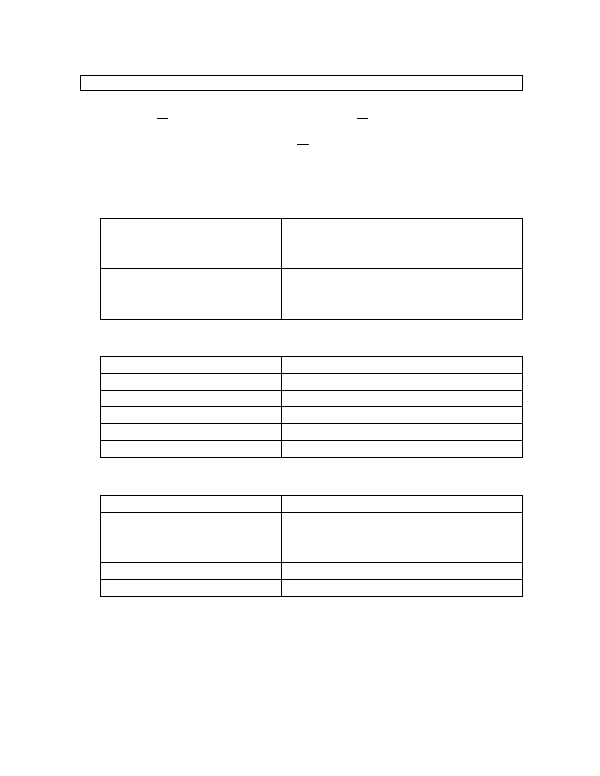
Instruction Set For 6420A
Instruction Op-Code Address Data
READ 1 0 1 0 1 0 0 0 A6 A5 A4 A3 A2 A1 A0 0 D15 -D0
WRITE 1 0 1 0 0 1 0 0 A6 A5 A4 A3 A2 A1 A0 0 D15 -D0
WREN 1 0 1 0 0 0 1 1
WRDS 1 0 1 0 0 0 0 0
( WRAL ) 1 0 1 0 1 1 1 1
эээХээХээХээХээХээХээХээХ
эээХээХээХээХээХээХээХээХ
эээ ХээХээХээХээХээХээХээХ
D15 -D0
Instruction Set For 6440A
Instruction Op-Code Address Data
READ 1 0 1 0 1 0 0 0 A7 A6 A5 A4 A3 A2 A1 A0 D15 -D0
WRITE 1 0 1 0 0 1 0 0 A7 A6 A5 A4 A3 A2 A1 A0 D15 -D0
WREN 1 0 1 0 0 0 1 1
WRDS 1 0 1 0 0 0 0 0
( WRAL ) 1 0 1 0 1 1 1 1
Instruction Set For 6480A
эээ ХээХээХээХээХээХээХээХ
эээ ХээХээХээХээХээХээХээХ
эээ ХээХээХээХээХээХээХээХ
D15 -D0
Instruction Op-Code Address Data
READ 1 0 1 0 1 0 0 A8 A7 A6 A5 A4 A3 A2 A1 A0 D15 -D0
WRITE 1 0 1 0 0 1 0 A8 A7 A6 A5 A4 A3 A2 A1 A0 D15 -D0
WREN 1 0 1 0 0 0 1 1
WRDS 1 0 1 0 0 0 0 0
( WRAL ) 1 0 1 0 1 1 1 1
(Note) The WRAL instruction is used for factory function test only. User can't use this instruction .
эээ ХээХээХээХээХээХээХээХ
эээ ХээХээХээХээХээХээХээХ
эээ ХээХээХээХээХээХээХээХ
D15 -D0
:don't care
Õ
DAS01E-00 1999/05
- 5 -
 Loading...