

AKM AK61584 Datasheet
ASAHI KASEI
[AK61584]
Features
- Provides Dual Analog PCM Line Interface
for short-haul,T1 and E1 applications
- Jitter Tolerance: Compliant with AT&T62411
TR-NWT-000499 Category
- Transmitter Pulse Shape: Compliant with
AT&T62411,CB119, TR-NWT-000499,
ITU-T G.703
- Jitter Transfer: AT&T62411, ITU-T G.736
- Operating mode fully software configurable.
No external quartz crystal
- Support of JTAG boundary scan
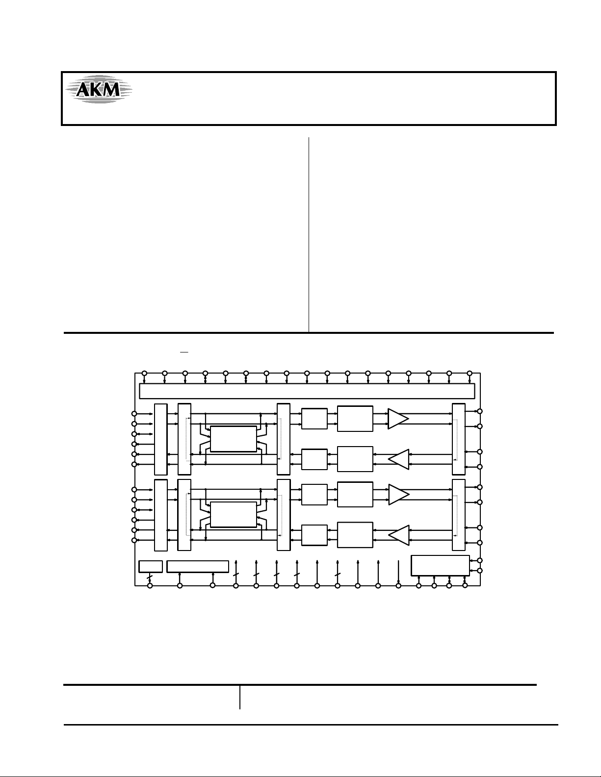
Serial Port
Hardware mode
IPOL (Note) CS INT SCLK
RLOOP2ATTEN0ATTEN1RLOOP1LLOOP1LLOOP2TAOS1TAOS2
I
,II ITU-T G.823
is required.
SDO SDI SPOL
AK61584
Dual Low Power T1/E1 Line Interface
- Low Power Consumption
- 3.3Volt operation
- Small Plastic Package 64pin LQFP(
1.4mm
)
10*10*
General Description
The AK61584 is a universal line interface for T1/E1 applications, designed for high-volume cards where low power,
high density and universal operation is required. One board
design can support all T1/E1 modes.
The AK61584 is a low-power CMOS device available
in 3.3 Volt.
CON01 CON02 CO N11 CON12 CON 21 CON22 COD ER1 CODER2 CLKE
TDATA1)TPOS 1
(
RDATA1)RPOS1
(
TDATA2)TPO S2
(
RDATA2)RPOS2
(
TCLK1
(AIS1)TNEG1
RCLK1
(BPV1)RNEG 1
TCLK2
(AIS2)TNEG2
RCLK2
(BPV2)RNEG2
ENCODER DECORDER
ENCODER DECORDER
JTAG
4
CONTROL
REMOTE LOOPBACK
JITTER
ATTENUATOR
REMOTE LOOPBACK
JITTER
ATTENUATOR
CLOCK GENERATOR
2
REFCLK 1XCLK TV+ TGND RV+ RGND DV+ DGND AV+ AG ND BGREF PD1 PD2 LOS1 LOS2
2
LOCAL LOOPBACK1
TAOS
LOS&
AIS
DETECT
LOCAL LOOPBACK1
TAOS
LOS&
AIS
DETECT
22
PULSE
SHAPING
CIRCUITRY
CLOCK&
DATA
RECOVERY
PULSE
SHAPING
CIRCUITRY
CLOCK&
DATA
RECOVERY
3
DRIVER
DRIVER
CONTROL
Note) In host mode, this pin must be tied to GND.
LOCAL LOOPBACK2
TTIP1
TRING1
RTIP1
RRING1
LOC AL LOO PBACK2
TTIP2
TRING2
RTIP2
RRING2
RESET
MODE
Preliminary Product Information
This document contains information for a new product. AKM
reserves the right to modify this product without notice.
0185-E-00 98/04
-1-

ASAHI KASEI
Table of Contents
Block Diagram................................................................................ 1
Specifications
General Description
Pin Description..............................................................................32
[AK61584]
Absolute Maximum Ratings............................................ 3
Recommended Operating Conditions .............................. 3
Digital Characteristics..................................................... 4
Analog Specifications
Receiver.............................................................. 4
Jitter Attenuator.................................................. 4
Transmitter ......................................................... 5
Switching Characteristics
T1 Clock/Data .................................................... 6
E1 Clock/Data .................................................... 6
Serial Port........................................................... 8
JTAG.................................................................. 9
Overview........................................................................10
Operating Options..........................................................11
Overview of Applications...............................................12
Transmitter.....................................................................13
Receiver.........................................................................15
Jitter Attenuator..............................................................16
Coder Mode...................................................................17
Reference Clock.............................................................17
Loopbacks......................................................................17
Power Down ..................................................................17
Reset..............................................................................18
Power-On Reset.............................................................18
Control...........................................................................18
Registers ........................................................................21
Host-Mode Register Access ...........................................23
Arbitrary Waveform Generation.....................................24
Power Supply.................................................................24
JTAG Boundary Scan.....................................................24
0185-E-00 98/04
-2-
ASAHI KASEI
[AK61584]
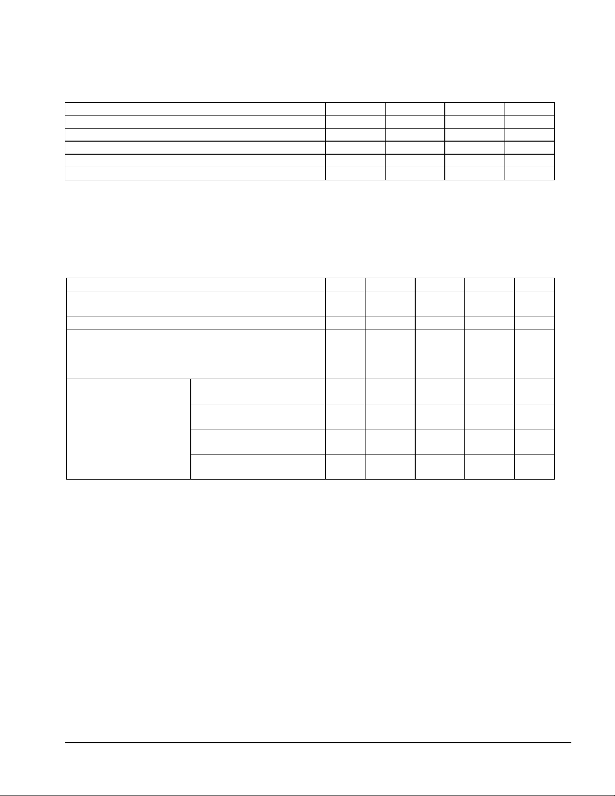
ABSOLUTE MAXIMUM RATINGS
Parameter Symbol Min Max Units
DC Supply(TV+1,TV+2,RV+1,RV+2,AV+,DV+)(Note 1) - 6.0 V
Input Voltage Any Pin Vin RGND-0.3 (RV+)+0.3 V
Input Current Any Pin (Note 2) Iin -10 10 mA
Ambient Operating Temperature TA -40 85
Storage Temperature Tstg -65 150
o
C
o
C
WARNING:Operations at or beyond these limits may result in permanent damage to the device.
Normal operation is not guaranteed at these extremes.
Notes: 1. Referenced to RGND1,RGND2,TGND1,TGND2,AGND,DGND at 0V.
2. Transient currents of up to 100 mA will not cause SCR latch-up.
RECOMMENDED OPERATING CONDITIONS
Parameter Symbol Min Typ Max Units
DC Supply(TV+1,TV+2,RV+1,RV+2,AV+,DV+)
(Note 3) 3.135 3.3 3.465 V
Ambient Operating Temperature TA -40 25 85
Power Consumption T1 (Notes 4 and 5)
(Each Channel) T1
(Notes 4 and 6)
E1,75ohm (Notes 4 and 5)
E1,120ohm (Notes 4 and 5)
REFCLK Frequency T1 1XCLK=1 1.544-
T1 1XCLK=0 12.352E1 1XCLK=1 2.048E1 1XCLK=0 16.384-
PC -
100ppm
100ppm
100ppm
100ppm
292
-
-
-
167
180
170
380
220
210
200
1.544 1.544+
100ppm
12.352 12.352+
100ppm
2.048 2.048+
100ppm
16.384 16.384+
100ppm
Notes: 3. TV+1,TV+2,AV+,DV+,RV+1,RV+2 should be connected together.TGND1,TGND2,RGND1,
RGND2,DGND1,DGND2,DGND3 should be connected together.
4. Power consumption while driving line load over operating temperature range. lncludes IC and load.
Digital input levels are within 10% of the supply rails and digital outputs are driving a 50 pF
capacitive load.
5. Assumes 100% ones density and maximum line length at 3.465V.
6. Assumes 50% ones density and 300ft. line length at 3.3V.
o
MW
MW
MW
MW
MHz
MHz
MHz
MHz
C
0185-E-00 98/04
-3-
ASAHI KASEI
[AK61584]
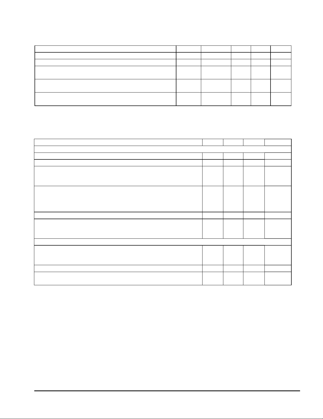
DIGITAL CHARACTERISTICS (TA=-40 to 85
o
C;power supply pins within +/-5% of nominal)
Parameter Symbol Min Typ Max Units
High-Level input Voltage (Note 7) VIH (DV+)-0.5 - - V
Low-Level input Voltage (Note 7) VIL - - 0.5 V
High-Level Output Voltage (Note 8)
VOH (DV+)-0.3 - - V
IOUT=-40uA
Low-Level Output Voltage (Note 8)
VOL - - 0.4 V
IOUT=1.6mA
Input Leakage Current
- - +/-10 uA
(Digital pins except INT, J_TMS, and J_TDI)
Notes: 7. Digital inputs are designed for CMOS logic levels.
8. Digital outputs are TTL compatible and drive CMOS levels into a CMOS load.
ANALOG SPECIFICATIONS (TA=-40 to 85
o
C;power supply pins within +/-5% of nominal)
Parameter Min Typ Max Units
Receiver
Input Impedance between RTIP/RRING - 20k - ohm
Sensitivity Below DSX-1(0 dB=2.4V) -13.6 - - DB
Loss of signal threshold, Short Haul
T1
E1
Data Decision Threshold T1,DSX-1 (Note 9)
(Note 10)
E1 (Note 11)
(Note 12)
60
55
45
40
-
-
0.23
0.15
65
-
50
-
70
75
55
60
-
-
V
V0p
0p
% of
Peak
Allowable Consecutive Zeros before LOS 160 175 190 bits
Receiver Input Jitter 10 Hz and below (Note 13)
Tolerance(DSX-1,E1) 2 kHz
10 kHz-100 kHz
300
6.0
0.4
-
-
-
-
-
-
UIpp
UIpp
UIpp
Jitter Attenuator
Jitter Attenuation Curve Corner Frequency (Note 14 and 15)
T1
E1
-
-
4
5.5
-
-
Hz
Hz
Attenuation at 10 kHz Jitter frequency (Note 14 and 15) - 60 - dB
Attenuator Input Jitter Tolerance (Note 14)
28 43 - UIpp
(Before Onset of FIFO Overflow or Underflow Protection)
Notes: 9. For input amplitude of 1.2Vpk to 4.14Vpk
10. For input amplitude of 0.5Vpk to 1.2Vpk, and 4.14Vpk to 5.0Vpk
11. For input amplitude of 1.07Vpk to 4.14Vpk
12. For input amplitude of 4.14Vpk to 5.0Vpk
13. Jitter tolerance increases at lower frequencies. See Figure 11.
14. Not production tested. parameters guaranteed by design and characterization.
15. Attenuation measured with sinusoidal input jitter equal to 3/4 of measured jitter tolerance.
Circuit attenuates jitter at 20 dB/decade above the corner frequency. See Figure 16. Output jitter
can increase significantly when more than 28 UI’s are input to the attenuator. See discussion in
jitter Attenuator section.
0185-E-00 98/04
-4-

ASAHI KASEI
[AK61584]
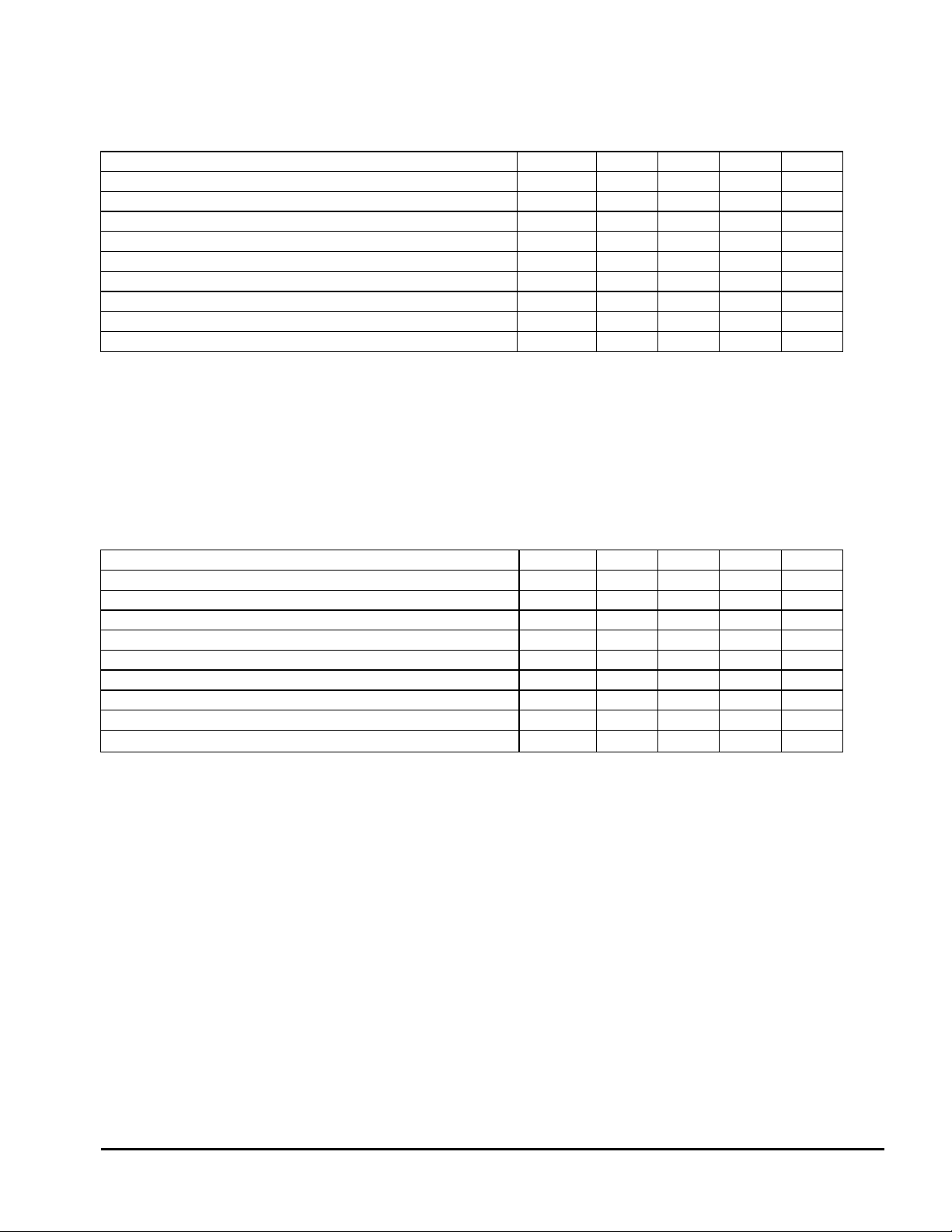
ANALOG SPECIFICATIONS (TA=-40 to 85
o
C;power supply pins within +/-5% of nominal)
Parameter Min Typ Max Units
Transmitter
AMI Output Pulse Amplitudes (Note 16)
E1,75ohm (Note 17)
E1,120ohm (Note 18)
T1,DSX-1 (Note 19)
2.14
2.7
2.4
2.37
3.0
3.0
2.6
3.3
3.6
V
0p
V0p
V0p
Recommended Transmitter Output Load (Note 16)
T1,
E1,75ohm
E1,120ohm
-
-
-
25
43
68.9
-
-
-
ohm
ohm
ohm
Jitter Added
by the Transmitter 8kHz – 40kHz
10Hz – 40kHz
Broad Band (Note 20)
Power in 2 kHz band about 772 kHz (Notes 14 and 21)
-
-
-
0.013
0.016
0.027
-
-
-
UI
pp
UIpp
UIpp
12.6 15 17.9 dBm
(DSX-1 only)
Power in 2 kHz band about 1.544 MHz (Notes 14 and 21)
-29 -38 - dB
(referenced to power in 2 kHz band at 772 kHz) (DSX-1 only)
Positive to Negative Pulse Imbalance (Notes 14 and 21)
T1,DSX-1
E1,amplitude at center of pulse interval
E1,width at 50% of nominal amplitude
-5
-5
-
0.2
-
-
0.5
+5
+5
dB
%
%
Transmitter Return Loss (Notes 14, 21, and 22)
51 kHz - 102 kHz
102 kHz - 2.048 MHz
2.048 MHz - 3.072 MHz
8
14
10
-
-
-
-
-
-
dB
dB
dB
E1 Short Circuit Current (Note 23) - - 50 mArms
E1 and DSX-1 Output Pulse Rise/Fall Times (Note 24) - 25 - ns
E1 Pulse Width (at 50% of peak amplitude) - 244 - ns
E1 Pulse Amplitude E1, 75ohm
for a space
E1,120ohm
-0.237
-0.3
-
-
0.237
0.3
0p
V
V0p
Notes: 16. Using a transformer that meets the specifications in Table 2.
17. Measured across 75ohm at the output of the transmit transformer for CON2/1/0=0/0/0.
18. Measured across 120ohm at the output of the transmit transformer for CON2/1/0=0/0/1.
19. Measured at the DSX-1 Cross-Connect for line length settings CON2/1/0=0/1/0, 0/1/1,
1/0/0, 1/0/1, and 1/1/0 after the length of #22 ABAM cable specified in Table 1.
20. Input signal to TCLK is jitter free.
21. Typical performance with a 0.47 uF capacitor in series with primary of transmitter output transformer.
22. Return loss = 20 log
Z
23. Transformer secondaries shorted with 0.5ohm resistor.
24. At transformer secondary. From 10% to 90% of amplitude.
=cable impedance.
0
ABS ((z1+z0)/(z1-z0)) where z1 = impedance of the transmitter, and
10
0185-E-00 98/04
-5-
ASAHI KASEI
[AK61584]
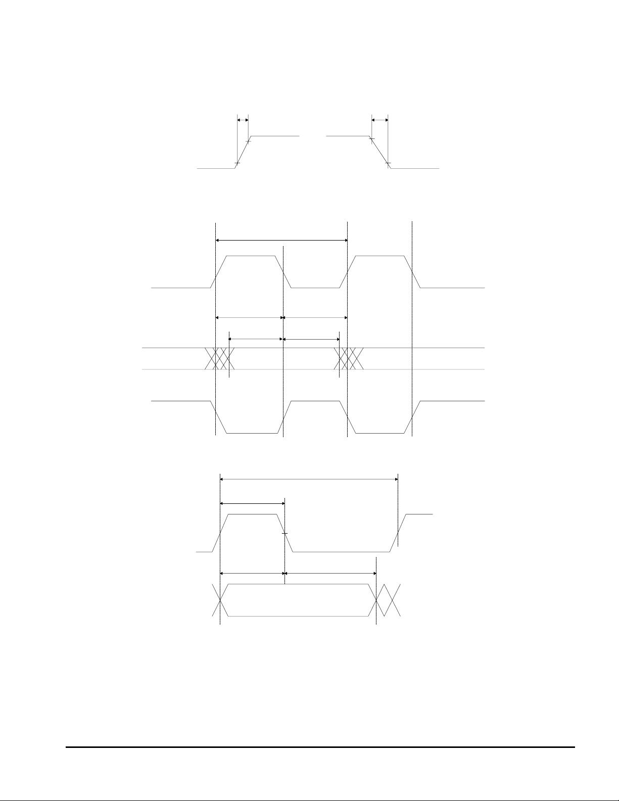
SWITCHING CHARACTERISTICS-T1 CLOCK/DATA (TA = -40 to 85
pins within +/-5% of nominal; Inputs: Logic 0=0V, logic 1=DV+)(See Figures 1,2, and 3)
o
C;power supply
Parameter Symbol Min Typ Max Units
TCLK Frequency (Note 25) ftclk - 1.544 - MHz
TCLK Duty Cycle tpwh2/tpw2 30 50 70 %
RCLK Duty Cycle (Note 26) tpwh1/tpw1 45 50 55 %
Rise Time All Digital Outputs (Note 27) tr --65ns
Fall Time All Digital Outputs (Note 27) tr --65ns
TPOS/TNEG to TCLK Falling Setup Time tsu2 25 - - ns
TCLK Falling to TPOS/TNEG Hold Time th2 25 - - ns
RPOS/RNEG to RCLK Rising Setup Time tsu1 - 274 - ns
RCLK Rising to RPOS/RNEG Hold Time th1 - 274 - ns
Notes: 25. Max value of 8.192 MHz describes the maximum burst rate of a gapped input clock(TCLK).
For the gapped clock to be tolerated by the AK61584, the jitter attenuator must be switched to
transmit path of the line interface. The maximum gap size is defined in the Analog Specification table.
26. RCLK duty cycle may be outside the spec limits when jitter attenuator is in the receive path,
and when the jitter attenuator is employing the overflow/underflow protection mechanism.
27. At max load of 50pF .
SWITCHING CHARACTERISTICS-E1 CLOCK/DATA (TA = -40 to 85
pins within +/-5% of nominal; Inputs: Logic 0=0V, Logic 1=DV+)(See Figures 1, 2, and 3)
o
C;power supply
Parameter Symbol Min Typ Max Units
TCLK Frequency (Note 25) ftclk - 2.048 - MHz
TCLK Duty Cycle tpwh2/tpw2 30 50 70 %
RCLK Duty Cycle (Note 26) tpwh1/tpw1 45 50 55 %
Rise Time All Digital Outputs (Note 27) tr --65ns
Fall Time All Digital Outputs (Note 27) tr --65ns
TOPS/TNEG to TCLK Falling Setup Time tsu2 25 - - ns
TCLK Falling to TOPS/TNEG Hold Time th2 25 - - ns
RPOS/RNEG to RCLK Rising Setup Time tsu1 - 194 - ns
RCLK Rising to RPOS/RNEG Hold Time th1 - 194 - ns
0185-E-00 98/04
-6-
ASAHI KASEI
[AK61584]
Any Digital O ut put
Figure 1. Signal Rise and Fall Characteristics
RCLK
(for CLK E =hig h)
RPOS
RNEG
(RDATA)
RCLK
(for CLK E =lo w )
tr
90%
10%
tpwl1
tsu 1
tf
90%
10%
tpw1
tpw h 1
th1
Figure 2. Recoverd Clock and Data Switching Characteristics
tpw 2
tpwh2
TCLK
tsu 2
th2
TPOS/TNEG
(TDATA)
Figure 3. Transmit Clock and Data Switching Characteristics
0185-E-00 98/04
-7-
ASAHI KASEI
[AK61584]
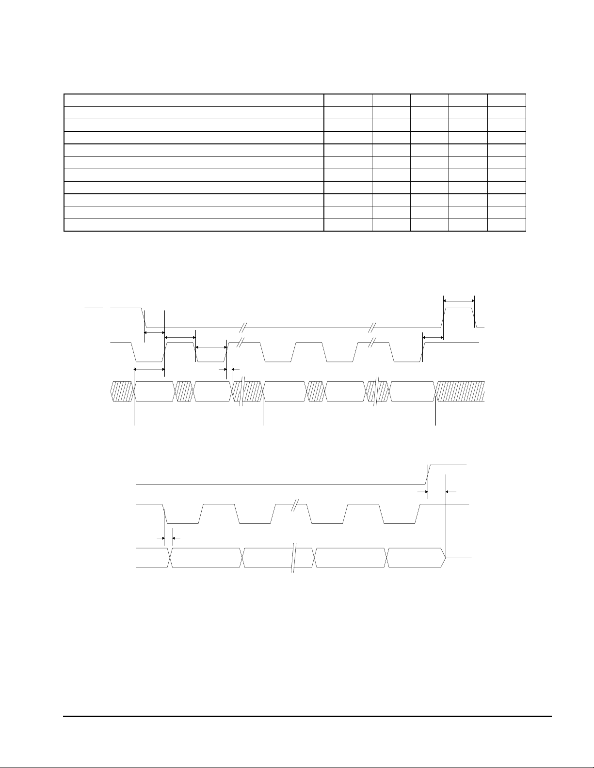
SWITCHING CHARACTERISTICS -SERIAL PORT (TA = -40 to 85
DV+,TV+,RV+ = nominal +/-0.3V; Inputs: Logic 0 = 0V, Logic 1 = RV+)
o
C;
Parameter Symbol Min Typ Max Units
SDI to SCLK Setup Time tdc 25 - - ns
SCLK to SDI Hold Time tcdh 25 - - ns
SCLK Low Time tcl 50 - - ns
SCLK High Time tcl 50 - - ns
SCLK Rise and Fall Time tr,tf --15ns
CS to SCLK Setup Time tcc 20 - - ns
SCLK to CS Hold Time (Note 28) tcch 20 - - ns
CS Inactive Time tcwh 100 - - ns
SCLK to SDO Valid (Note 29) tcdv --50ns
CS to SDO High Z tcdz -50-ns
Notes: 28. If SPOL=0, then CS should return high no sooner than 20ns after the 16‘th falling edge of SCLK
during a serial port read.
29. Output load capacitance = 50 pF.
tcwh
CS
tcc
tch
tcl
tcch
SCLK
SDI
SCLK
SPOL= 0
CS
SDO
tdc
LSB
CONTROL BYTE
tcdh
LSB
MSB
DATA BYTE
Figure 4. Serial Port Write Timing Diagram
tcdv
Figure 5. Serial Port Read Timing Diagram
tcdz
High-Z
0185-E-00 98/04
-8-
ASAHI KASEI
[AK61584]
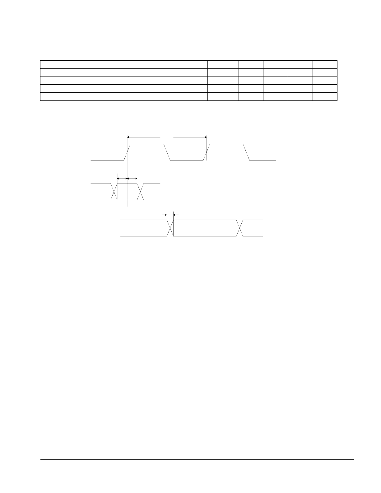
SWITCHING CHARACTERISTICS -JTAG (TA = -40 to 85
TV+,RV+ = nominal +/-0.3V; Inputs: Logic 0 = 0V, Logic 1 =RV+)
o
C;
Parameter Symbol Min Typ Max Units
Cycle Time tcyc 200 - - ns
J_TMS/J_TDI to J_TCK rising setup time tsu 50 - - ns
J_CLK rising to J_TMS/J_TDI hold time th 50 - - ns
J_TCLK falling to J_TDO valid tdv --50ns
tcyc
J_TCK
tsu
th
J_TM S
J_TDI
tdv
J_TD O
Figure 6. JTAG Swithing Characteristics
0185-E-00 98/04
-9-
ASAHI KASEI
[AK61584]
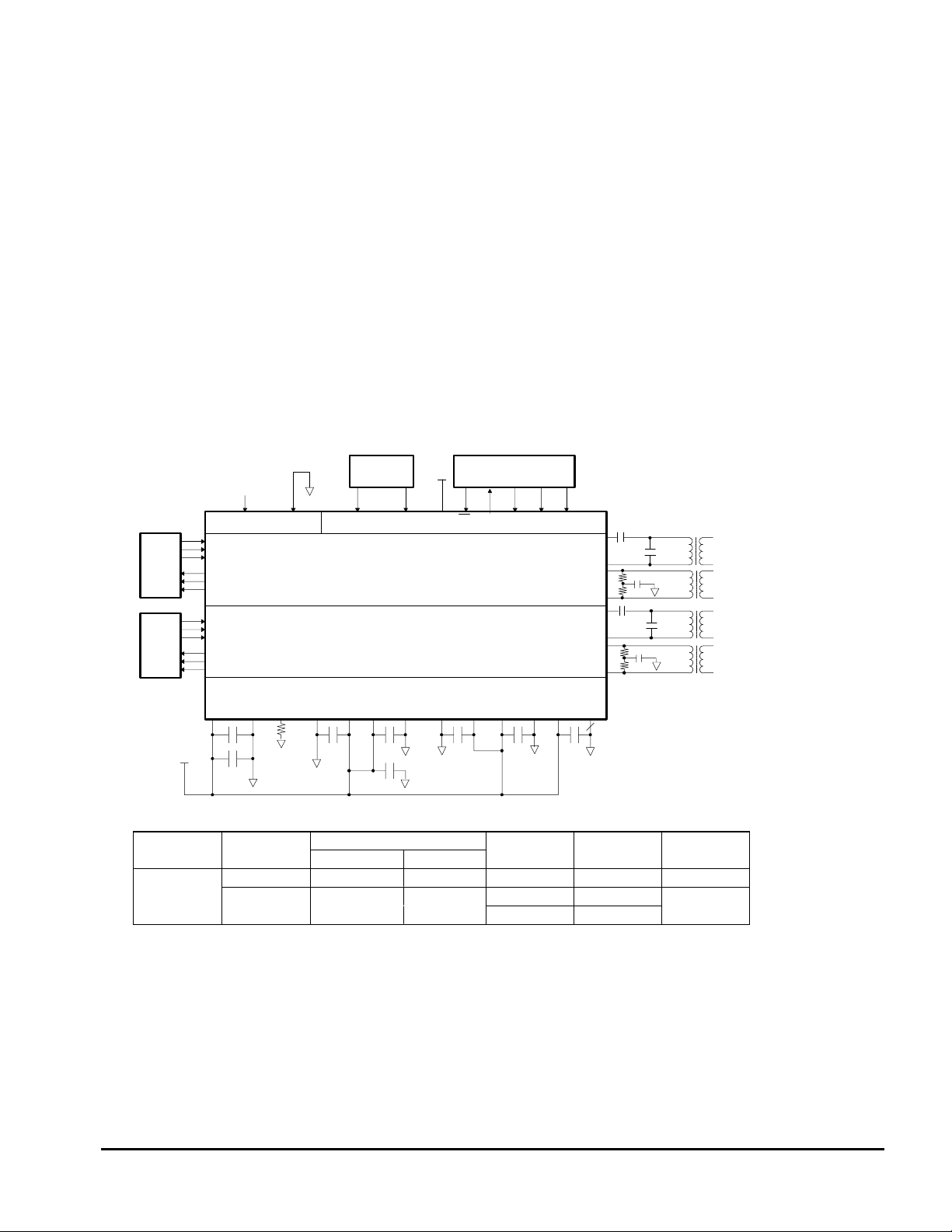
OVERVIEW
The AK61584 is a universal line interface for
T1/E1 applications, designed for high-volume cards
where low power, high density and universal operation is required. One board design
can support
all T1/E1 short-haul modes. The T1 and E1 modes
can be selected entirely via software.
As shown in Figure 1, the AK61584 provides all
the functions needed for a line interface
including a
line driver, a receiver and jitter attenuator.
The line driver generates waveforms compatible
with E1 (ITU-T G.703),T1 short haul (DSX-1).
Framer
Framer
12.352MHz
REFCLK
TCLK1
TPOS1
TNEG1
RCLK1
RPOS1
RNEG1
TCLK2
TPOS 2
TNEG2
RCLK2
RPOS2
RNEG2
Clock
Clock
1XCLK
Control
IPOL RESET
Channel 1
Channel 2
Power Supply
VCC
MODE INTCSSCLK
Control
The driver internally matches the impedance of the
load, providing excellent return loss. The benefit of
the internal impedance matching is a 50 percent
reduction in power consumption compared to implementing return loss with external resistors. With
external
resistors a driver has to drive the equiva-
lent of two line loads.
The receiver contains clock and data recovery circuits.
The jitter attenuator meets AT&T 62411 requirements without the use of an external quartz crystal.
The attenuator does require an external reference
clock.
Micro Controller
serial port
SDI
SDO
TRING1
RRING1
TRING2
RRING2
TTIP1
RTIP1
TTIP2
RTIP2
R1
R2
R3
R4
0.47uF
470pF
(E1)
0.47uF
0.47uF
470pF
(E1)
0.47uF
T1
transmit
1:N
T2
receive
1:N
T3
transmit
1:N
T4
receive
1:N
Vcc
AV+
AGND
+
0.1uF
1uF
BGREF
R3
5kohm
TGND2 TV+2 TV+1
0.1uF
0.1uF
+
22uF
TGND1
RGND2
0.1uF
RV+2
RV+1
RGND1
0.1uF
DV+
DGND
3
0.01uF
Vcc Data Rate REFCLK Frequency MHz Cable R1-R4 Transformers
Volts MHz 1XCLK=1 1XCLK=0 ohm ohm T1-T4
1.544 1.544 12.352 100 12.5 1:2
3.3 2.048 2.048 16.384 75 21.5 1:1.32
120 34.4
Figure 7 - Typical Connection Diagram
( Host Mode)
0185-E-00 98/04
-10-

ASAHI KASEI
[AK61584]
OPERATING OPTIONS
The following are the major operating options which
are supported by the AK61584:
Control
Control of the AK61584 is via either host mode (seri-
al port) or hardware mode (individual control lines).
Hardware mode offers significantly fewer programmability options than the host mode.
T1/E1
The AK61584 supports T1 short-haul (DSX-1), and
E1 operation. The configuration pins (CON <0:2>)
and register bits control transmitted pulse shapes,
transmitter source impedance, and receiver slicing
level. Both channels must be operated at the same
rate (both T1 or both E1).
The pulse shapes are fully pre-defined by circuitry in
the AK61584, and are fully compliant with appropriate standards when used with our application guidelines in standard installations.
T1/E1 framing device. Alternatively, a coder mode
can be selected. In coder mode, an internal
B8ZS/AMI/HDB3 coder can be used on those systems which don't need T1/E1
framers (typically
high-speed multiplexers). In host mode, the choice of
transmit encoder is independent of the choice of receiver decoder.
Reference Clock
The AK61584 requires a T1 or E1 reference clock.
This clock can be either a 1-X clock (i.e.,1.544 MHz
or 2.048MHz). or can be a 8-X clock (i.e., 12.352
MHz or 16.384 MHz). In systems which want software selection of data rate, the
1-X clock option is
typically chosen, and the reference clock is tied to the
transmit clock. In systems with a jittered transmit
clock, an external oscillator should drive the reference
clock input, and a 8-X rate can be used to minimize
the physical size of the oscillator. In either case, any
jitter present on the reference clock will not be filtered
by the jitter attenuator, and the reference clock should
have 100 ppm or better frequency accuracy.
Power Down
The transmitter impedance changes with the line
length options in order to match the impedance of the
load (75-ohm for E1 coax, 100-ohm for T1, 120- ohm
for E1 Shielded twisted pair).
receiver slicing level is set at 65% for DSX-1
The
short-haul, and at 50% for all other applications.
Line Codes
The AK61584 supports a transparent mode where
the line code is encoded and decode by an external
Either one of the two line interfaces may be independently powered down.
Jitter Attenuator
The jitter attenuator may be placed in the receiver
path, the transmit path or bypassed entirely.
0185-E-00
98/04
-11-
ASAHI KASEI
OVERVIEW OF APPLICATIONS
This section summarizes a typical application of the
AK61584 in various environments, and discusses
what AK61584 options would normally be selected
in that application. See Figure 8.
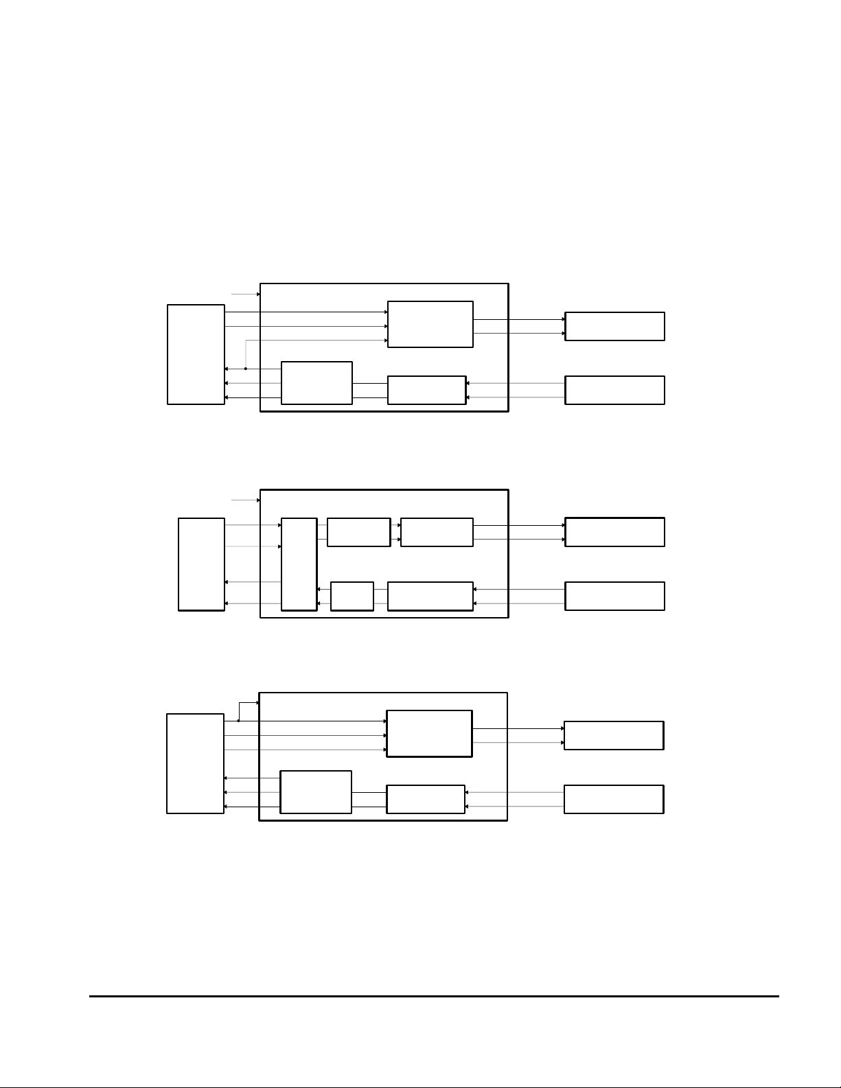
AT&T 62411 APPLICATION
(Systems with a single T1 line)
12.352MHz ±32ppm
TPOS
TNEG
CS2180B
FRAMER
CIRCUIT
TCLK
RCLK
RPOS
RNEG
REFCLK
JITTER
ATTENUATOR
AK61584
AT&T 62411 Customer Premises Application
AT&T 62411 applies at the T1 interface between
the customer premises and the carrier, and must be
implemented by the customer premises equipment.
LINE DRIVER
LINE RECEIVER
TTIP
TRING
RTIP
RRING
[AK61584]
TRANSMIT
TRANSFORMER
RECEIVE
TRANSFORMER
12.352MHz ±100ppm
TDATA
TCLK
(gapped)
MUX
RCLK
RDATA
CS2180B
FRAMER
CIRCUIT
Figure 8. Configuration Examples for Various Applicatons
ASYNCHRONOUS MUX APPLICATION
(for example, VT 1.5 card for SONET or SDH mux)
REFCLK
AMI
B8ZS
HDB3
CODER
(including 62411 systems with multiple T1 lines)
REFCLK
JITTER
ATTENUATOR
AK61584
JITTER
ATTENUATOR
AIS
DETECT
SYNCHRONOUS APPLICATION
AK61584
LINE DRIVER
LINE RECEIVER
LINE DRIVER
LINE RECEIVER
TTIP
TRING
RTIP
RRING
TTIP
TRING
RTIP
RRING
TRANSMIT
TRANSFORMER
RECEIVE
TRANSFORMER
TRANSMIT
TRANSFORMER
RECEIVE
TRANSFORMER
0185-E-00
-12-
98/04
 Loading...