

AKM AK6003A Datasheet
ASAHI KASEI [AK6003A]
AK6003A
Software Write Protect I2C bus 2Kbit EEPROM
Features
ADVANCED CMOS EEPROM TECHNOLOGY
READ/WRITE NON-VOLATILE MEMORY
WIDE VCC OPERA TION Vcc = 1.8V 5.5V
2048 bits, 2568 organization
2CTM
I
SERIAL INTERFACE
LOW POWER CONSUMPTION
- 0.8A Max. Standby
HIGH RELIABILITY
- Endurance : 100K cycles
- Data Retention : 10 years
16 byte page write mode
Software Write Protection (lower 128 bytes)
Hardware Write Protection (entire array)
Automatic write cycle time-out with auto-ERASE
IDEAL FOR LOW DENSITY DATA STORAGE
- Low cost, space saving, 8-pin package (TSSOP)
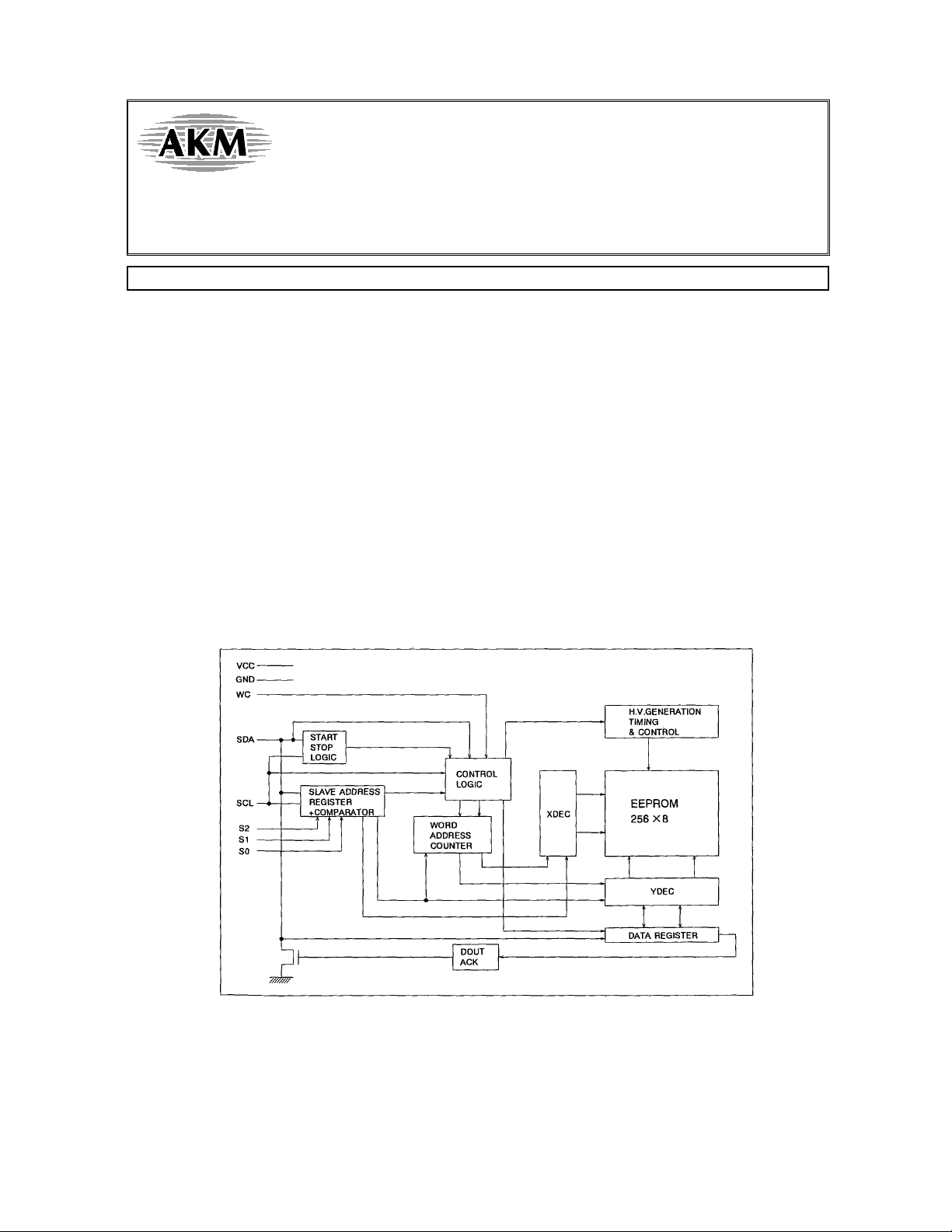
Block Diagram
2CTM
I
is a registered trademark of Philips Corporation.
DAI03E-01 1999/10
- 1 -
ASAHI KASEI [AK6003A]
General Description
The AK6003A is a 2048-bit serial CMOS E2PROM divided into 256 registers of 8 bits each.
The AK6003A can operate full function under wide operating voltage range from 1.8V to 5.5V. The
charge up circuit is integrated for high voltage generation that is used for write operation.
The AK6003A conforms to all specifications in the 2 wire protocol and is controlled by serial clock
(SK) and serial data (SDA) line.
Some devices can be connected to the same bus. Each device connected to the bus is software
addressable by a unique address, and can operate as either a transmitter or receiver. In addition to
transmitters and receivers, devices can also be considered as masters or slaves when performing
data transfers (see Table1). The master is the device which initiates a data transfers on the bus and
generates the clock signals to permit that transfer. At that time, the device addressed is considered
as the slave.
TERM DESCRIPTION
Transmitt er The device which sends the data to the bus
Receiver The device which receives the data from the bus
Master The device which initiates a transfer, generates clock signals and terminates
a transfer
Slave The device addressed by a master
Table 1. Definitions
Write protection
Hardware Write Protection
If WC pin is High level, WRITE operations onto the entire array will not be executed. If the WC pin is
Low level, the AK6003A will be enabled to perform WRITE operation.
As the WC pin is internally pulled down to GND, the AK6003A will be enabled to perform WRITE
operation if the WC pin is left floating.
Software Write Protection
The software write protect register is programmed by sending a software write protect command
and the software write protection is enabled.
If the software write protection is enabled, Write operations onto the lower half of the array($00$7F)
will not be executed permanently. Once the software write protect register has been programmed,
the write protection can not be reversed. The software write protection can not be reversed even if
the AK6003A is powered down.
If the WC pin is high level, WRITE operations onto the entire array will not be executed regardless of
the status of the software protection.
Type of Products
Model Memory size Temp.Range Vcc Package
AK6003AV 2Kbits -40C85C1.8V
5.5V 8pin Plastic TSSOP
DAI03E-01 1999/10
- 2 -
ASAHI KASEI [AK6003A]
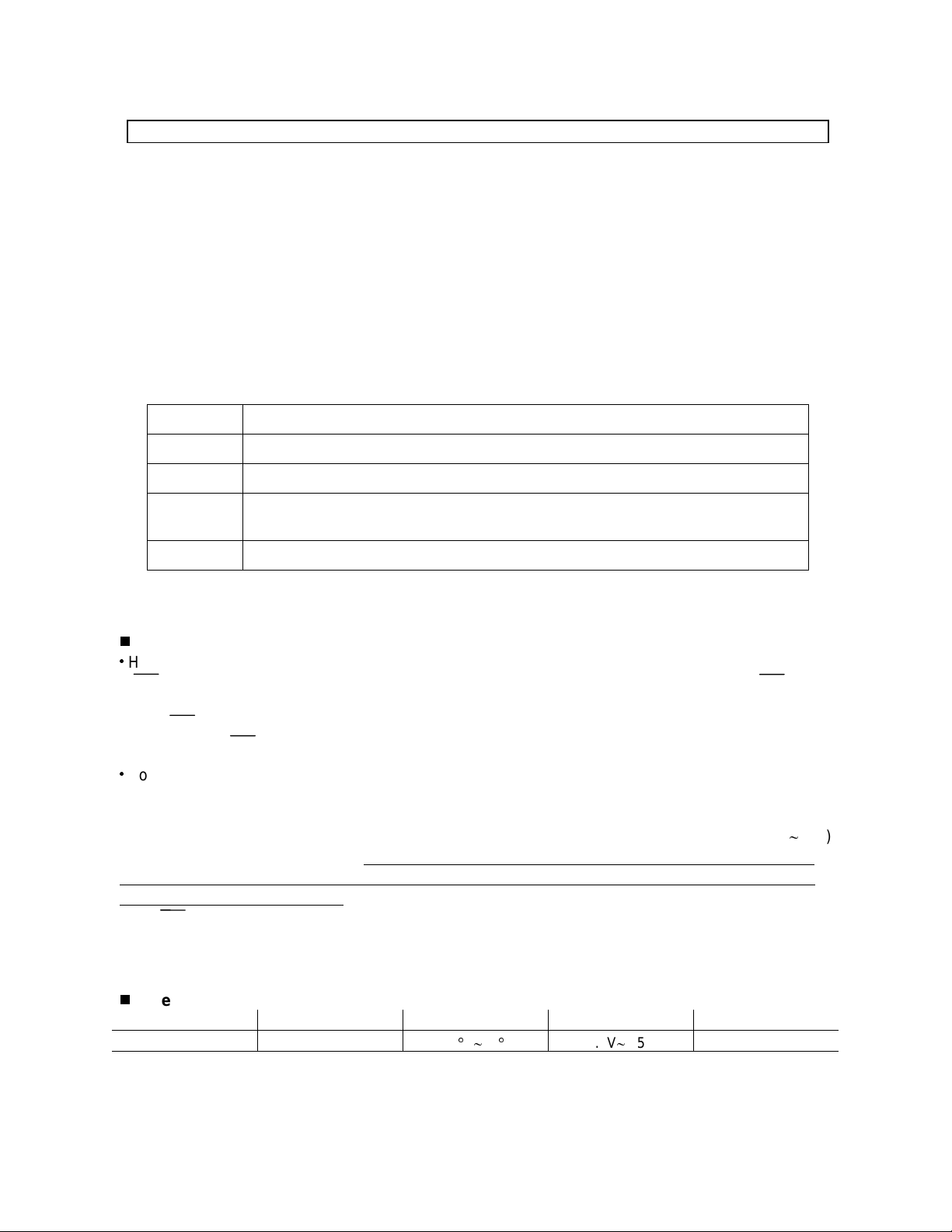
Pin arrangement
Pin Name Function
S0,S1,S2 Device Address Inputs
SCL Clock Input
SDA Data Input / Output
WC Write Control
Vcc Power Supply
GND Ground
DAI03E-01 1999/10
- 3 -
ASAHI KASEI [AK6003A]
DATA TRANSFER
All commands are preceded by a START condition. After the START condition, a slave address is
sent. After the AK6003A recognizes the START condition, the devices interfaced to the bus wait for
the slave address to be transmitted over the SDA line. If the transmitted slave address matches an
address of one of the device, the designated slave pulls the SDA line to LOW (ACKNOWLEDGE) .
The data transfer is always terminated by a STOP condition generated by the master.
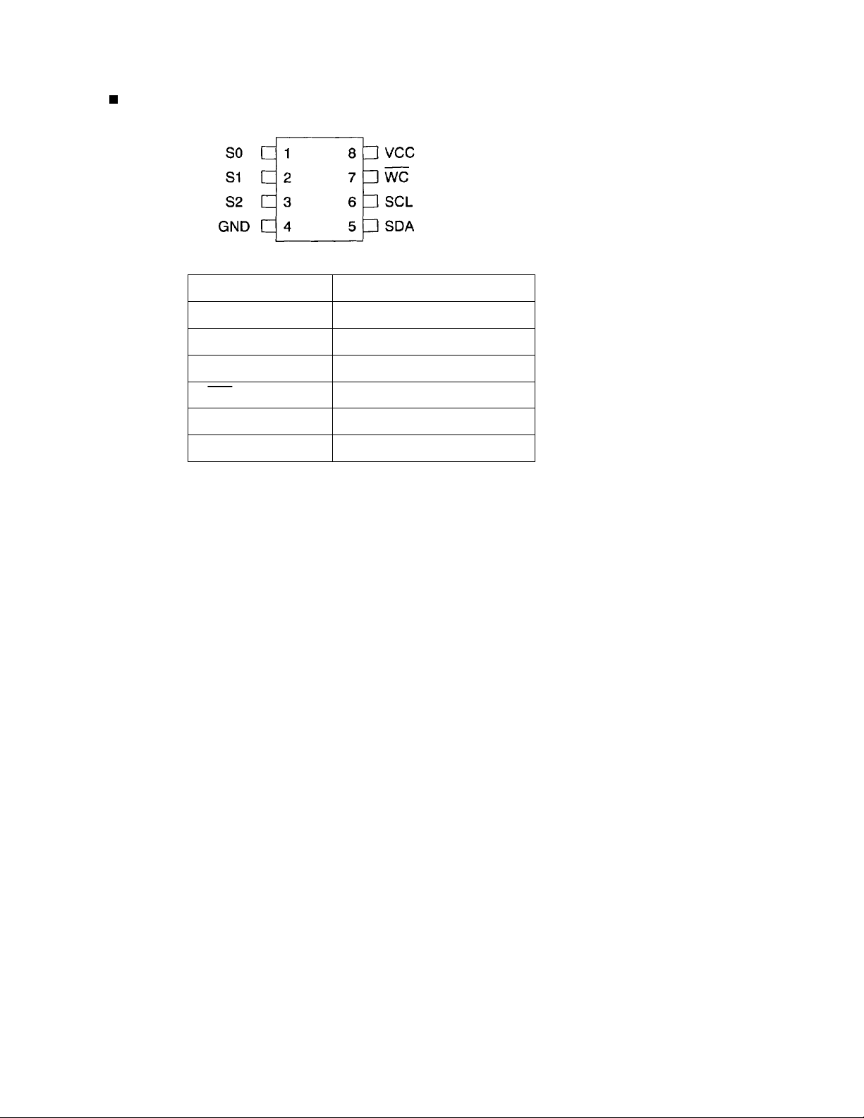
[ Data validity ]
The data on the SDA line must be stable during the HIGH period of the clock. The HIGH or LOW
state of the data line can only change when the clock signal on the SCL line is LOW.
Figure1. Data transfer
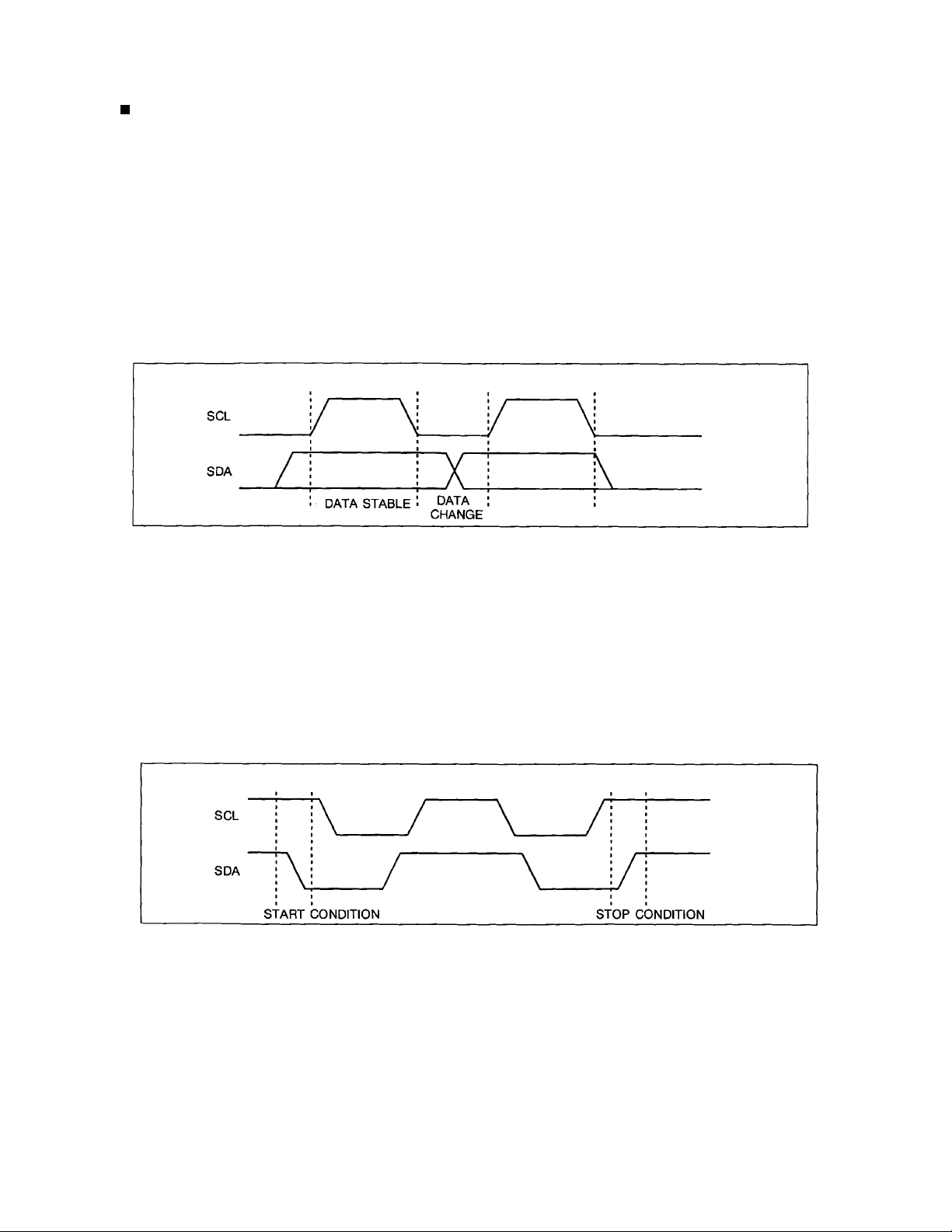
[ START and STOP condition]
A HIGH to LOW transition on the SDA line while SCL is HIGH defines a START condition. All
commands are preceded by the START condition.
A LOW to HIGH transition on the SDA line while SCL is HIGH defines a STOP condition. All
communications are terminated by the STOP condition. After a read sequence, the STOP condition
will place the EEPROM in a standby power mode.
Figure2. Start and STOP Definition
DAI03E-01 1999/10
- 4 -
ASAHI KASEI [AK6003A]
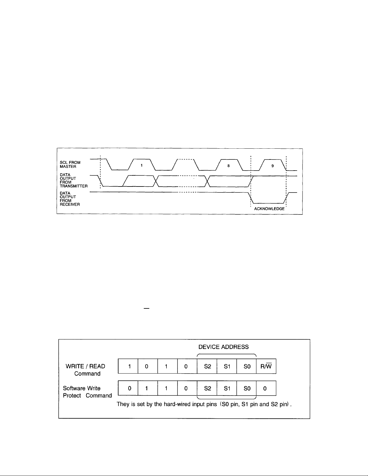
[ACKNOWLEDGE]
ACKNOWLEDGE is a software convention used to indicate successful data transfers. The
transmitting device will release the bus after transmitting eight bits. During the next clock (ninth
clock), the receiver will pull the SDA line to LOW to acknowledge that it received the eight bits of
data.
The AK6003A will respond with an acknowledge after recognition of a start condition and its slave
address. If both the device and a write operation have been selected, the AK6003A will respond
with an acknowledge after the receipt of each subsequent eight bit word.
In the read mode the AK6003A slave will transmit eight bits of data, release the SDA line and
monitor the line for an acknowledge. If an acknowledge is detected and no STOP condition is
generated by the master, the slave will continue to transmit data. If an acknowledge is not detected,
the slave will terminate further data transmissions and await the STOP condition to return to the
standby power mode.
Figure3. Acknowledge Response from Receiver
[SLAVE ADDRESS]
After the START condition, a SLAVE ADDRESS is sent. If the transmitted slave address matches an
address of one of the device, the designated slave pulls the SDA line to LOW .
The most significant four bits of the slave address are "1010" or "0110". The next three bits are S0,
S1 and S2 device address bits. These three bits identify the specific device on the bus. They is set
by the hard wired input pins (S0 pin, S1 pin and S2 pin). Therefore a total of eight devices can be
connected to the same bus.
The last bit of the slave address (R/W bit) defines whether a write or read condition is requested by
the master. A "1" indicates that the read operation is to be executed. A "0" indicates that the write
operation is to be executed.
Figure4. Slave Address
DAI03E-01 1999/10
- 5 -

ASAHI KASEI [AK6003A]
Pin Descriptions
(Serial Clock)
SCL
The SCL input is used to clock all data into and out of the device.
(Serial Data)
SDA
The SDA is a bidirectional pin used to transfer data into and out of the device.
It is an open drain output and may be wire-ORed with any number of open drain or open collector
outputs.
S0, S1, S2
The S0, S1 and S2 are device address inputs that are used to set three bits of the slave address. A
total of eight devices can be connected to the same bus.
WC (Write Control)
If the WC is High level, WRITE operations will not be executed. If the WC is Low level, the AK6003A
will be enabled to perform WRITE operation.
As the WC is internally pulled down to GND, the AK6003A will be enabled to perform WRITE
operation if the WC is left floating.
WC must not change from the start condition input to the stop condition input.
(Power Supply)
VCC
GND
(Device Address)
(Ground)
DAI03E-01 1999/10
- 6 -
 Loading...