

AKM AK5354 Datasheet
ASAHI KASEI [AK5354]
AK5354
Low Power 20bit ∆Σ ADC with PGA
FEATURES
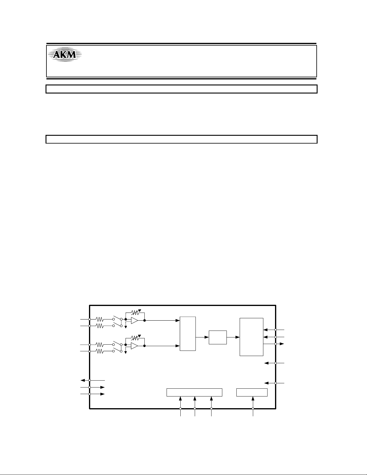
The AK5354 is a low voltage 20bit A/D converter for digital audio system. The AK5354 also includes
Analog input PGA, therefore is suitable for microphone application and etc. As digital power supply of the
AK5354 corresponds to 1.8V, the interface with microprocessor can operate at low voltage. Analog
signal input of the AK5354 is single-ended, therefore, any external filters are not required. As the
package is 16pin TSSOP, the AK5354 is a suitable for minimizing system.
FEATURES
1. Resolution : 20bits
2. Recording Functions
• 2-Stereo Inputs Selector
• Analog Input PGA
• Monaural Mixing
• Digital HPF for DC-offset cancellation (fc=3.4Hz@fs=44.1kHz)
3. ADC Characteristics
• Input Level : 1.5Vpp@VA=2.5V (= 0.6 x VA)
• S/(N+D) : 84dB
• DR, S/N : 89dB
4. 3-wire Serial Control I/F
5. Master Clock : 256fs/384fs
6. Audio Data Format : MSB First, 2’s compliment
• 20bit MSB justified or I
8. Power Supply
• VA : 2.1 ∼ 3.3V (typ. 2.5V)
• VD : 1.8 ∼ 3.3V (typ. 2.5V)
9. Power Supply Current
• IPGA + ADC : 7mA
10. Ta = -40 ∼ 85°C
11. Package : 16pin TSSOP
2
S
LIN1
LIN2
RIN1
RIN2
VCOM
VA
VSS
IPGA
ADC
HPF
Control Register I/F Clock Divider
CSN CCLK CDTI MCLK
Audio I/F
Controller
LRCK
BCLK
SDTO
VD
PDN
MS0054-E-01 2001/01
- 1 -
ASAHI KASEI [AK5354]
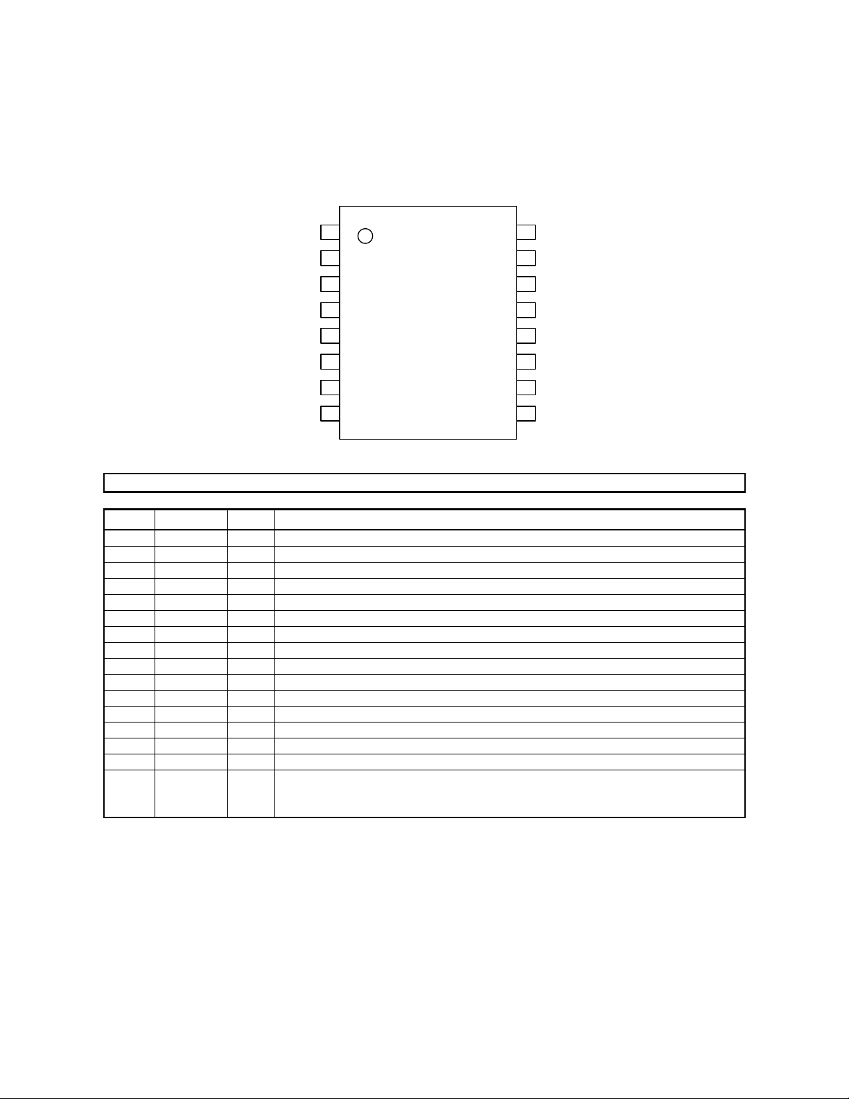
n Ordering Guide
AK5354VT -40 ∼ +85°C 16pin TSSOP (0.65mm pitch)
AKD5354 Evaluation Board for AK5354
n Pin Layout
LIN1
RIN1
LIN2
RIN2
VCOM
VSS
VA
VD
No. Pin Name I/O Function
1 LIN1 I Lch #1 Input Pin
2 RIN1 I Rch #1 Input Pin
3 LIN2 I Lch #2 Input Pin
4 RIN2 I Rch #2 Input Pin
5 VCOM O ADC Common Voltage Output Pin
6 VSS - Ground Pin
7 VA - Analog Power Supply Pin, +2.5V
8 VD - Digital Power Supply Pin, +2.5V
9 SDTO O Audio Serial Data Output Pin
10 BCLK I Audio Serial Data Clock Pin
11 MCLK I Master Clock Input Pin
12 LRCK I Input/Output Channel Clock Pin
13 CDTI I Control Data Input Pin
14 CCLK I Control Clock Input Pin
15 CSN I Chip Select Pin
Reset & Power Down Pin
16 PDN I
“L” : Reset & Power down
“H” : Normal operation
1
2
3
4
Top View
5
6
7
8
PIN/FUNCTION
16
15
14
13
12
11
10
9
PDN
CSN
CCLK
CDTI
LRCK
MCLK
BCLK
SDTO
Note: All digital input pins should not be left floating.
MS0054-E-01 2001/01
- 2 -

ASAHI KASEI [AK5354]
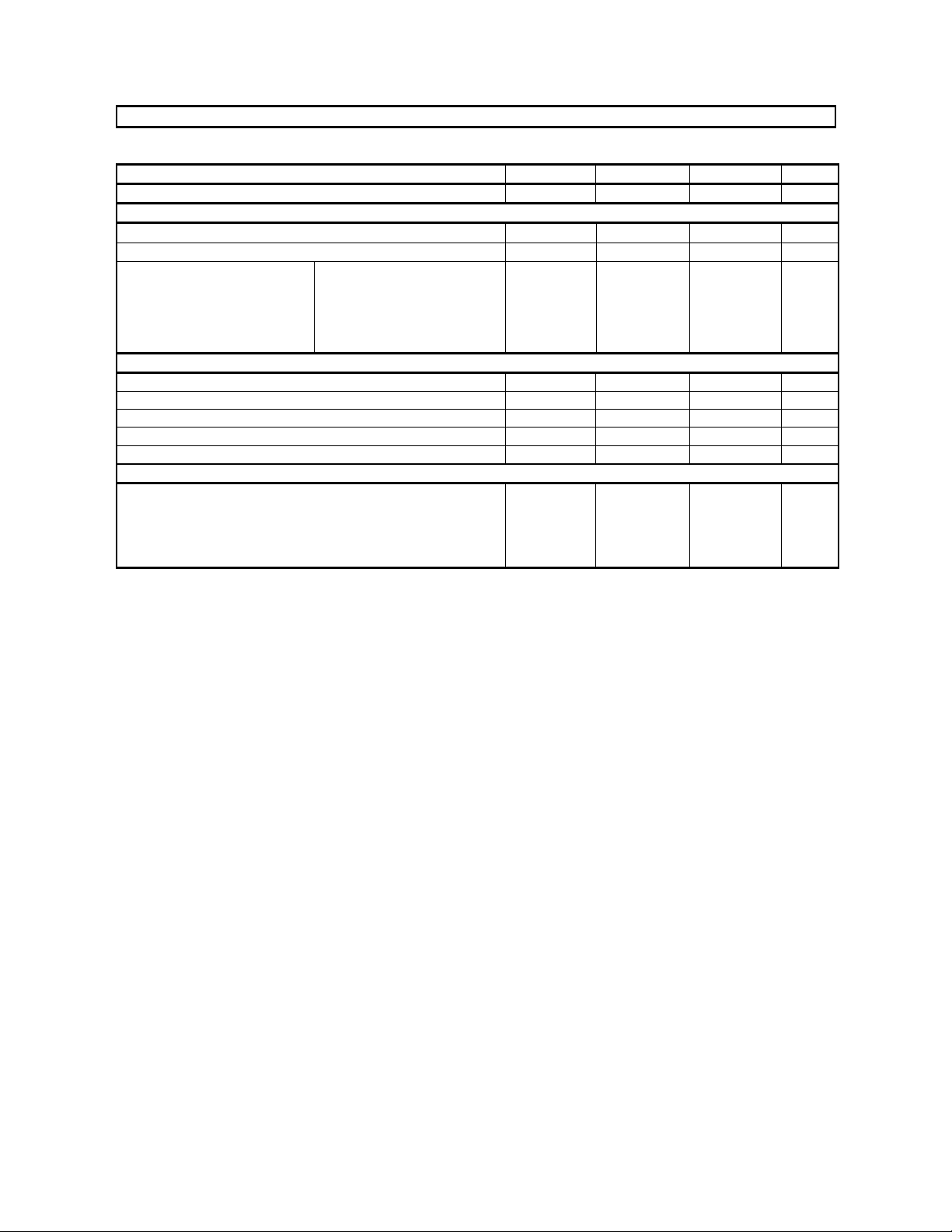
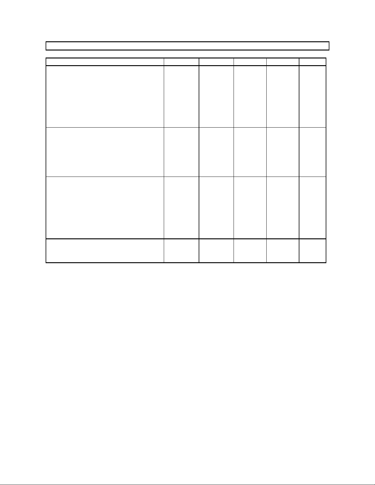
ABSOLUTE MAXIMUM RATINGS
(VSS=0V; Note 1)
Parameter Symbol min max Units
Power Supply Analog
Digital
Input Current (Any Pin Except Supplies) IIN Analog Input Voltage (LIN2-1, RIN2-1 pins) VINA -0.3 VA+0.3 V
Digital Input Voltage VIND -0.3 VD+0.3 V
Ambient Temperature (power applied) Ta -40 85
Storage Temperature Tstg -65 150
Note: 1. All voltages with respect to ground.
WARNING: Operation at or beyond these limits may results in permanent damage to the device.
Normal operation is not guaranteed at these extremes.
VA
VD
-0.3
-0.3
4.6
4.6
±10
V
V
mA
°C
°C
RECOMMENDED OPERATING CONDITIONS
(VSS=0V; Note 1)
Parameter Symbol min typ max Units
Power Supply Analog (VA pin)
Digital (VD pin)
VA
VD
2.1
1.8
2.5
2.5
3.3
VA
V
V
Note: 1. All voltages with respect to ground.
WARNING: AKM assumes no responsibility for the usage beyond the conditions in this data sheet.
MS0054-E-01 2001/01
- 3 -
ASAHI KASEI [AK5354]
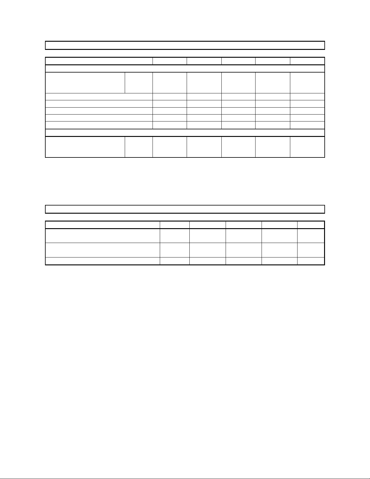
ANALOG CHARACTERISTICS
(Ta=25°C; VA, VD=2.5V; fs=44.1kHz; Signal Frequency=1kHz; Measurement frequency=10Hz ∼ 20kHz;
unless otherwise specified)
Parameter min typ max Units
Resolution 20 bits
Input PGA Characteristics (IPGA):
Input Voltage (LIN1, LIN2, RIN1, RIN2) (Note 2) 1.35 1.5 1.65 Vpp
Input Impedance 6.3 9 15
Step Width
ADC Analog Input Characteristics: (Note 3)
S/(N+D) (-0.5dBFS Input) 74 84 dB
D-Range (EIAJ) 82 89 dB
S/N (EIAJ) 82 89 dB
Interchannel Isolation 90 100 dB
Interchannel Gain Mismatch 0.2 0.5 dB
Power Supplies
Power Supply Current: VA+VD
Normal Operation (PDN=“H”)
IPGA+AD (PM0=1, PM1=1)
Power Down (PDN=“L”) (Note 4)
+28dB ∼ -8dB
-8dB ∼ -16dB
-16dB ∼ -32dB
-32dB ∼ -40dB
-40dB ∼ -52dB
0.1
0.1
0.1
0.5
1
2
-
-
2
4
7
10
1
2
4
-
-
10
100
kΩ
dB
dB
dB
dB
dB
mA
µA
Note: 2. Analog input voltage (full-scale voltage: IPGA = 0dB) scale with VREF. (IPGA = ADC = 0.6 x VREF)
Note: 3. ADC is input from LIN1/RIN1 or LIN2/RIN2 and it measures included in IPGA. The value of IPGA is set 0dB.
Internal HPF cancels the offset of IPGA and ADC.
Note: 4. In case of power-down mode, all digital input pins including clocks pins (MCLK, BCLK and LRCK) are held
VD or VSS. PDN pin is held VSS.
MS0054-E-01 2001/01
- 4 -
ASAHI KASEI [AK5354]
FILTER CHARACTERISTICS
(Ta=25°C; VA=2.1 ∼ 3.3V, VD=1.8 ∼ 3.3; fs=44.1kHz)
Parameter Symbol min typ max Units
ADC Digital Filter (Decimation LPF):
Passband (Note 5)
Stopband (Note 5) SB 27.0 kHz
Passband Ripple PR
Stopband Attenuation SA 65 dB
Group Delay (Note 6) GD 17.0 1/fs
Group Delay Distortion
ADC Digital Filter (HPF):
Frequency Response (Note 5) -3dB
Note:5. The passband and stopband frequencies scale with fs (sampling frequency).
For examples, PB=0.454 x fs(@ADC: -1.0dB), PB=0.454 x fs(@DAC: -0.1dB).
Note: 6. The calculating delay time which occurred by digital filtering. This time is from the input of analog signal to
setting the 20bit data of both channels to the output register for ADC and include group delay of HPF.
±0.1dB
-1.0dB
-3.0dB
-0.5dB
-0.1dB
PB 0
∆GD
FR 3.4
20.0
21.1
0
10
22
17.4 kHz
kHz
kHz
±0.1
dB
µs
Hz
Hz
Hz
DC CHARACTERISTICS
(Ta=25°C; VA=2.1 ∼ 3.3V, VD=1.8 ∼ 3.3V)
Parameter Symbol min Typ max Units
High-Level Input Voltage
Low-Level Input Voltage
High-Level Output Voltage (Iout=-80µA)
Low-Level Output Voltage (Iout=80µA)
Input Leakage Current Iin - -
VIH
VIL
VOH
VOL
75%VD
-
VD-0.4
-
-
-
--
-
25%VD
0.4
± 10 µA
V
V
V
V
MS0054-E-01 2001/01
- 5 -
ASAHI KASEI [AK5354]
SWITCHING CHARACTERISTICS
(Ta=25°C; VA=2.1 ∼ 3.3V, VD=1.8 ∼ 3.3V; CL=20pF)
Parameter Symbol min typ max Units
Control Clock Frequency
Master Clock (MCLK) 256fs: Frequency
Pulse Width Low
Pulse Width High
384fs: Frequency
Pulse Width Low
Pulse Width High
Channel Clock (LRCK) Frequency
Duty Cycle
Audio Interface Timing
BCLK Period
BCLK Pulse Width Low
Pulse Width High
BCLK “↓” to LRCK
LRCK Edge to SDTO (MSB)
BCLK “↓” to SDTO
Control Interface Timing
CCLK Period
CCLK Pulse Width Low
Pulse Width High
CDATA Setup Time
CDATA Hold Time
CSN “H” Time
CSN “↓” to CCLK “↑”
CCLK “↑” to CSN “↑”
Reset / Calibration Timing
PDN Pulse Width
PDN “↑” to SDTO (Note 7)
fCLK
tCLKL
tCLKH
fCLK
tCLKL
tCLKH
fs
tBLK
tBLKL
tBLKH
tBLR
tDLR
tDSS
tCCK
tCCKL
tCCKH
tCDS
tCDH
tCSW
tCSS
tCSH
tPW
tPWV
2.048
28
28
3.072
23
23
8
45
312.5
130
130
-tBLKH+50 tBLKL-50
200
80
80
50
50
150
50
50
150
11.2896
16.9344
44.1
4128
12.8
19.2
50
55
80
80
MHz
ns
ns
MHz
ns
ns
kHz
%
ns
ns
ns
ns
ns
ns
ns
ns
ns
ns
ns
ns
ns
ns
ns
1/fs
Note: 7. These cycles are the numbers of LRCK rising from PDN pin rising.
MS0054-E-01 2001/01
- 6 -
 Loading...