

AKM AK5353VT Datasheet
ASAHI KASEI [AK5353]
L
AK5353
96kHz 24Bit ∆Σ ADC with Single–ended Input
GENERAL DESCRIPTION
The AK5353 is a stereo A/D Converter with wide sampling rate of 4kHz∼96kHz and is suitable for
multimedia audio system. The AK5353 achieves high accuracy and low cost by using Enhanced dual bit
∆Σ techniques. The AK5353 requires no external components because the analog inputs are singleended. The audio interface has two formats (MSB justified, I
Karaoke, surround.
FEATURES
o Stereo ∆Σ ADC
o On-Chip Digital Anti-Alias Filtering
o Single-ended Input
o Digital HPF for DC-Offset cancel
o S/(N+D): 84dB@5V, 80dB@3V for 48kHz
o DR: 96dB@5V, 92dB@3V for 48kHz
o S/N: 96dB@5V, 92dB@3V for 48kHz
o Sampling Rate Ranging from 4kHz to 96kHz
o Master Clock:
256fs/384fs/512fs (∼48kHz)
256fs/384fs (∼96kHz)
o Low Power Dissipation: 70mW
o Small 16pin TSSOP Package
o Power Supply: 2.7∼5.5V (∼48kHz)
4.5∼5.5V (∼96kHz)
o Ta=-40∼85°C
o Input level: TTL/CMOS selectable
o Output format: 24bit MSB justified / I
2
S) and can correspond to many systems like
2
S selectable
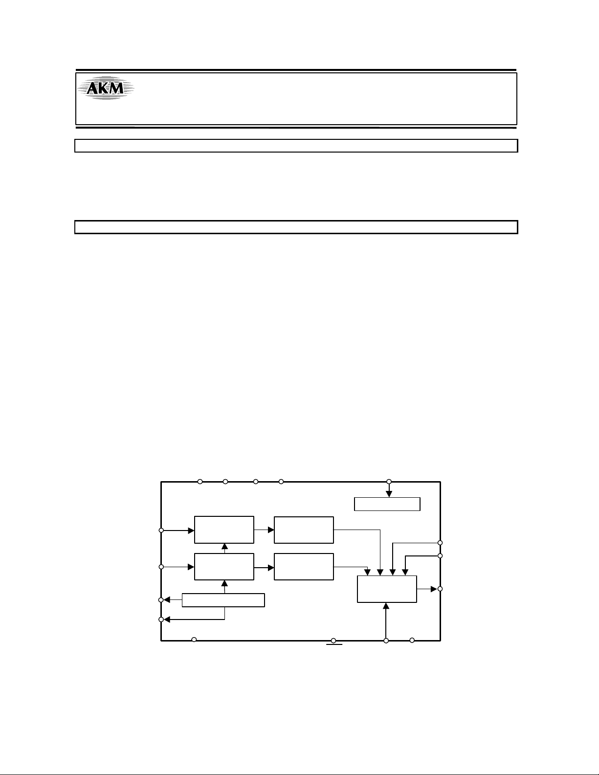
MCLK
Clock Divider
Serial I/O
Interface
DIF
LRCK
SCLK
SDTO
TTL
AIN
AINR
VCOM
VREF
AGNDVA
∆Σ
Modulator
∆Σ
Modulator
Voltage Reference
TST
DGNDVD
Decimation
Filter
Decimation
Filter
PD
M0067-E-00 1999/06
- 1 -
ASAHI KASEI [AK5353]
n Ordering Guide
AK5353VT -40∼+85°C 16pin TSSOP
AKD5353 Evaluation Board
n Pin Layout
AINL
VREF
VCOM
AGND
VA
VD
DGND
1AINR
2
3
4
Top
16
15
14
13
TST
TTL
DIF
PDN
View
5
6
7
8
12
11
10
SCLK
MCLK
LRCK
9
SDTO
M0067-E-00 1999/06
- 2 -
ASAHI KASEI [AK5353]
PIN/FUNCTION
No. Pin Name I/O Description
1 AINR I Rch Analog Input Pin
2 AINL I Lch Analog Input Pin
3 VREF O Voltage Reference Output Pin
Normally connected to AGND with a 0.1uF ceramic capacitor
in parallel with an electrolytic capacitor less than 4.7uF.
4 VCOM O Common Voltage Output Pin
Normally connected to AGND with a 0.1uF ceramic capacitor
in parallel with an electrolytic capacitor less than 4.7uF.
5 AGND - Analog Ground Pin, 0V
6VA 7VD -
Analog Power Supply Pin, +2.7∼+5.5V
Digital Power Supply Pin, +2.7∼+5.5V
8 DGND - Digital Ground Pin, 0V
9 SDTO O Serial Data Output Pin
Data bits are presented MSB first, in 2 s complement format.
This pin is L in the power-down mode.
10 LRCK I Left/Right Channel Select Pin
The fs clock is input to this pin.
11 MCLK I Master Clock Input Pin
SCLK I Serial Data Input Pin
12
Output data is clocked out on the falling edge of SCLK.
13 PDN I Power-Down Pin
When L , the circuit is in power-down mode.
The AK5353 should always be reset upon power-up.
14 DIF I Serial Interface Format Pin
L : MSB justified, H : I
2
S
15 TTL I Digital Input Level Select Pin
L : CMOS level (VA,VD=2.7∼5.5V), H : TTL level (VA,VD=4.5∼5.5V)
16 TST I Test Pin (Internal pull-down pin)
This pin should be left floating.
Note: All input pins except pull-down pins should not be left floating.
M0067-E-00 1999/06
- 3 -

ASAHI KASEI [AK5353]
ABSOLUTE MAXIMUM RATINGS
(AGND, DGND=0V; Note 1)
Parameter Symbol min max Units
Power Supplies Analog (VA pin)
Digital (VD pin)
|AGND-DGND|
Input Current (any pins except for supplies) IIN Analog Input Voltage (AINL, AINR pins) VINA -0.3 VA+0.3 V
Digital Input Voltage VIND -0.3 VD+0.3 V
Ambient Temperature Ta -40 85
Storage Temperature Tstg -65 150
Note:1. All voltages with respect to ground.
2. AGND and DGND must be connected to the same analog ground plane.
WARNING: Operation at or beyond these limits may results in permanent damage to the device.
Normal operation is not guaranteed at these extremes.
VA
VD
∆GND
-0.3
-0.3
-
6.0
6.0
0.3
±10
V
V
V
mA
°C
°C
RECOMMENDED OPERATING CONDITIONS (fs=48kHz)
(AGND, DGND=0V; Note 1)
Parameter Symbol min typ max Units
Power Supplies
(Note 3)
Sampling Rate fs 4 48 kHz
Analog
Digital
VA
VD
2.7
2.7
5.0
5.0
5.5
VA
V
V
Note:1. All voltages with respect to ground.
3. The power up sequence between VA and VD is not critical.
RECOMMENDED OPERATING CONDITIONS (fs=96kHz)
(AGND, DGND=0V; Note 1)
Parameter Symbol min typ max Units
Power Supplies
(Note 3)
Sampling Rate fs 4 96 kHz
Note:1. All voltages with respect to ground.
3. The power up sequence between VA and VD is not critical.
*AKM assumes no responsibility for the usage beyond the conditions in this datasheet.
Analog
Digital
VA
VD
4.5
4.5
5.0
5.0
5.5
VA
V
V
M0067-E-00 1999/06
- 4 -
ASAHI KASEI [AK5353]
ANALOG CHARACTERISTICS
(Ta=25°C; VA,VD=5V; fs=48kHz; I/F format=Mode 0; Signal Frequency =1kHz;
Measurement band width=20Hz∼20kHz; unless otherwise specified)
Parameter min typ max Units
ADC Analog Input Characteristics: Analog source impedance=470Ω (BW=40Hz∼40kHz at fs=96kHz)
Resolution 24 Bits
S/(N+D) (-1dBFS) (Note 4) fs=48kHz, VA=5V
fs=48kHz, VA=3V
fs=96kHz, VA=5V
DR (-60dBFS) (Note 5) fs=48kHz, VA=5V, A-weighted
fs=48kHz, VA=3V, A-weighted
fs=96kHz, VA=5V
S/N fs=48kHz, VA=5V, A-weighted
fs=48kHz, VA=3V, A-weighted
fs=96kHz, VA=5V
Interchannel Isolation 78 90 dB
DC Accuracy
Interchannel Gain Mismatch 0.1 0.3 dB
Gain Drift 100 150
Input Voltage (Note 6) 2.7 3.0 3.3 Vpp
Input Resistance (Note 7) 40 60
Power Supply Rejection (Note 8) - 30 dB
Power Supplies
Power Supply Current
Normal Operation (PDN= H )
VA+VD (Note 9)
Power-Down Mode (PDN= L )
VA+VD
76
76
90
86
90
86
84
84
-
-
-
84
96
92
93
96
92
93
14
10
21
100
dB
dB
dB
dB
dB
dB
dB
dB
dB
ppm/°C
kΩ
mA
µA
Note:4. The ratio of the rms value of the signal to the rms sum of all the spectral components less than 20kHz bandwidth,
including distortion components.
5. S/(N+D) which is measured with an input signal of -60dB below full-scale.
6. This value is the full scale(0dB) of the input voltage.
Input voltage is proportional to VA. (Vin=0.6xVA)
7. 40kΩ(typ) and 25kΩ(min) at fs=96kHz.
8. PSR is applied to VA,VD with 1kHz, 50mVpp.
9. VA=11mA; VD=3mA@48kHz,5V, 1.5mA@48kHz,3V, 6mA@96kHz,5V (typ).
M0067-E-00 1999/06
- 5 -
ASAHI KASEI [AK5353]
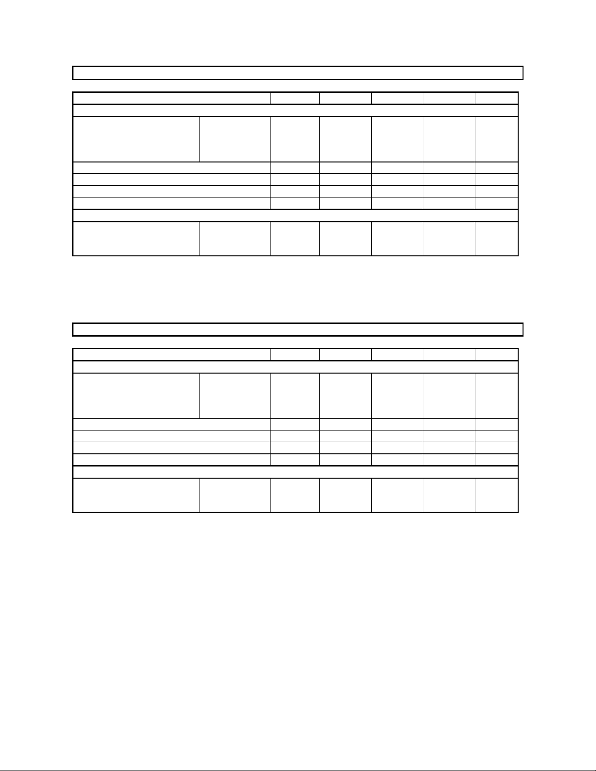
FILTER CHARACTERISTICS (fs=48kHz)
(Ta=25°C; VA,VD=2.7∼5.5V; fs=48kHz)
Parameter Symbol min typ max Units
Digital Fi l te r (Decimation LPF)
Passband (Note 10)
Stopband (Note 10) SB 29.4 kHz
Stopband Attenuation SA 65 dB
Group Delay Distortion
Group Delay (Note 11) GD - 17.0 - 1/fs
Digital F i l t e r (HPF)
Frequency Response: -3 dB
Note:10. The passband and stopband frequencies scale with fs.
11. The calculating delay time which occurred by digital filtering. This time is from the input of analog signal
to setting the 24bit data of both channels to the output register for ADC.
±0.1dB
-0.2dB
-1.0dB
-3.0dB
-0.5dB
-0.1dB
PB 0
∆GD
FR -
18.9
-
-
-
-
-
20.0
21.8
23.0
0
4
11
24
-
-
-
-
-
-
kHz
kHz
kHz
kHz
µs
Hz
Hz
Hz
FILTER CHARACTERISTICS (fs=96kHz)
(Ta=25°C; VA,VD=4.5∼5.5V; fs=96kHz)
Parameter Symbol min typ max Units
Digital Fi l te r (Decimation LPF)
Passband (Note 10)
Stopband (Note 10) SB 58.8 kHz
Stopband Attenuation SA 65 dB
Group Delay Distortion
Group Delay (Note 11) GD - 17.0 - 1/fs
Digital F i l t e r (HPF)
Frequency Response: -3 dB
Note:10. The passband and stopband frequencies scale with fs.
11. The calculating delay time which occurred by digital filtering. This time is from the input of analog signal
to setting the 24bit data of both channels to the output register for ADC.
±0.1dB
-0.2dB
-1.0dB
-3.0dB
-0.5dB
-0.1dB
PB 0
∆GD
FR -
37.8
-
-
-
-
-
40.0
43.6
46.0
0
8
22
48
-
-
-
-
-
-
kHz
kHz
kHz
kHz
µs
Hz
Hz
Hz
M0067-E-00 1999/06
- 6 -
 Loading...