

AKM AK5351-VF Datasheet
ASAHI KASEI [AK5351]
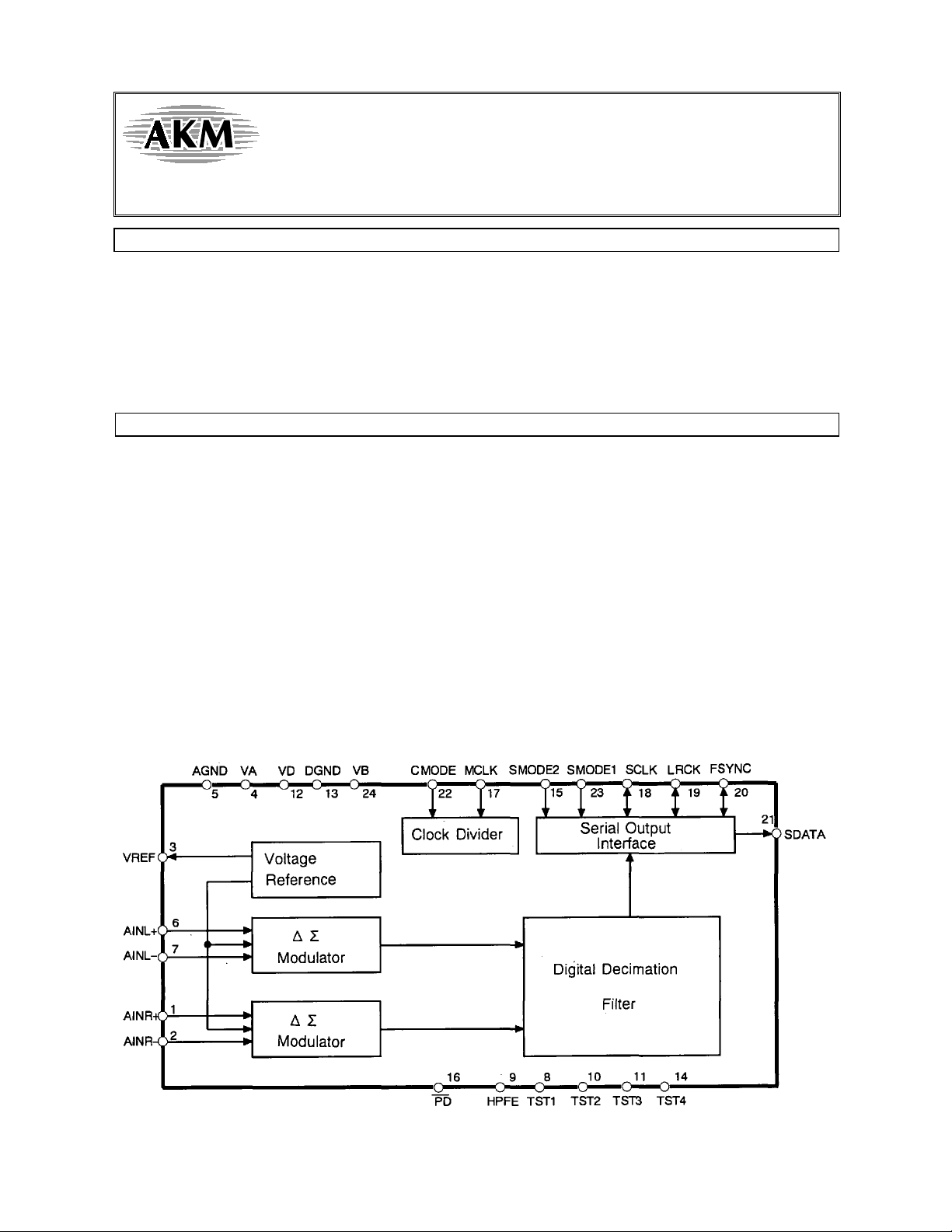
GENERAL DESCRIPTION
The AK5351 is a 20-bit, 64x oversampling rate(64fs), 2-channel A/D converter for stereo digital systems.
The ∆Σ modulator in the AK5351 uses the new developed Enhanced Dual bit architecture. This new
architecture achieves the wider dynamic range, while keeping much the same superior distortion
characteristics as the conventional Single bit way. The AK5351 is suitable for digital surround and Hi-Fi
audio application such as Car-audio, MD, etc. Analog inputs of the AK5351 are normally Full-differential inputs,
while they are also acceptable Single-ended inputs.
The AK5351 is available in a small 24pin VSOP package which will reduce your system space.
FEATURES
Enhanced Dual bit ∆Σ 20bit ADC
AK5351
Full-differential / Single-ended inputs
S/(N+D): 97dB
DR, S/N: 103dB
Linear phase digital filter
Pass band: 0~22kHz(@fs=48kHz)
Pass band ripple: ±0.005dB
Stop band attenuation: 80dB
Digital HPF for DC-offset cancel
Master clock: 256fs/384fs
Power supply: 5V±10%
Small package: 24pinVSOP
0166-E-00 1997/4
- 1 -
ASAHI KASEI [AK5351]
Ordering Guide
AK5351-VF -40~85°C 24pin VSOP
AKD5351/2 Evaluation Board
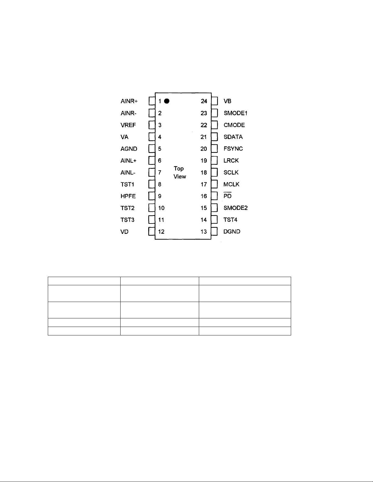
Pin Layout
Replacement from AK5350 to AK5351
AK5350 AK5351
Package 28VSOP 24VSOP
*)Interchangeable with AK5350
Analog Inputs Voltage
fc of HPF(@fs=48kHz) 7Hz 1Hz
SCLK ~64fs ~128fs
±3.47Vp-p ±2.10Vp-p
*)Acceptable Single-ended
0166-E-00 1997/4
- 2 -
ASAHI KASEI [AK5351]
PIN/FUNCTION
No. Pin Name I/O FUNCTION
1 AINR+ I Right channel analog positive input pin
2 AINR- I Right channel analog negative input pin
3 VREF O Voltage Reference output pin (VA-2.6V)
Normally connected to VA with a 0.1uF ceramic capacitor in
parallel with a 10uF electrolytic capacitor.
4 VA - Analog section Analog Power Supply, +5V
5 AGND - Analog section Analog Ground
6 AINL+ I Left channel analog positive input pin
7 AINL- I Left channel analog negative input pin
8
10
11
14
TST1
TST2
TST3
TST4
Test pin (Pull-down pin)
Should be left floating.
9 HPFE I High Pass Filter Enable pin (Pull-up pin)
"H": ON
"L": OFF
12 VD - Digital section Digital Power Supply pin, +5V
13 DGND - Digital section Digital Ground pin
16 PD I Power Down pin
"L" brings the device into power-down mode. Must be done
once after power-on.
17 MCLK I Master Clock input pin
CMODE="H":384fs
CMODE="L":256fs
18 SCLK I/O Serial Data Clock pin
Data is clocked out at the falling edge of SCLK.
Slave mode: 64fs clock is input usually.
Master mode: SCLK outputs a 64fs clock.
SCLK stays low during the power-down mode(PD="L").
19 LRCK I/O L/R Channel Clock Select pin
Slave mode: An fs clock is fed to this LRCK pin.
Master mode: LRCK output an fs clock.
LRCK goes "H" at SMODE2="L" and "L" at SMODE2="H"
during reset when SMODE1 "H".
20 FSYNC I/O Frame Synchronization Signal pin
Slave mode: When "H", data bits are clocked out on SDATA.
2
As I
S slave mode ignores FSYNC, it should hold "L" or
"H".
Master mode: FSYNC outputs 2fs clock.
Stay low during the power-down mode(PD="L").
0166-E-00 1997/4
- 3 -
ASAHI KASEI [AK5351]
21 SDATA O Serial Data Output pin
Data are output with MSB first, in 2's complement format.
After 20 bits are output it turns to "L". It also remains "L" at a
power-down mode(PD="L").
22 CMODE I Master Clock Selection pin
"L": MCLK=256fs
"H": MCLK=384fs
23
15
SMODE1
SMODE2
I
Serial Interface Mode Select pin
I
Defines the directions of LRCK, SCLK and FSYNC pins and
Output Data Format. SMODE2 is pull-down pin.
SMODE1 SMODE2 MODE LRCK
L L Slave mode: MSB justified : H/L
2
H L Master mode: Similar to I
L H Slave mode: I
H H Master mode: I
2
S : L/H
2
S : L/H
S : H/L
24 VB - Substrate Power Supply, +5V
0166-E-00 1997/4
- 4 -

ASAHI KASEI [AK5351]
ABSOLUTE MAXIMUM RATINGS
(AGND,DGND=0V; Note 1 )
Parameter Symbol min max Units
DC Power Supply:Analog Power(VA pin)
Digital Power(VD pin) (Note 2 )
Substrate Power(VB pin)
Input Current (Any pin except supplies) IIN Analog Input Voltage
VA
VD
VB
-0.3
-0.3
-0.3
6.0
6.0/VB+0.3
6.0
10
±
mA
VINA -0.3 6.0/VA+0.3 V
V
V
AINL+,AINL-,AINR+,AINR-pins (Note 2 )
Digital Input Voltage (Note 2 ) VIND -0.3 6.0/VB+0.3 V
°
Ambient Temperature Ta -40 85
Storage Temperature Tstg -65 150
C
°
C
Note 1 : All voltage with respect to ground.
Note 2 : Absolute maximum value is the highest voltage in 6.0V, VA+0.3V and VB+0.3V.
WARNING: Operation beyond these limits may result in permanent damage to the device.
Normal operation is not guaranteed at these extremes.
RECOMMENDED OPERATING CONDITIONS
(AGND,DGND=0V; Note 1 )
Parameter Symbol min typ max Units
DC Power Supplies: Analog Power
Digital Power(VD pin)
(VB pin) (Note 3 )
VA
VD
VB
4.50
4.50
4.50
5.0
5.0
5.0
5.50
VB
5.50
Note 1 : All voltages with respect to ground.
Note 3 : The VA and VB are connected together through the chip substrate and have several ohms
resistance. The VA and VB should be powered at the same time or earlier than VD.
* AKM assumes no responsibility for the usage beyond the conditions in this data sheet.
V
V
V
0166-E-00 1997/4
- 5 -
ASAHI KASEI [AK5351]
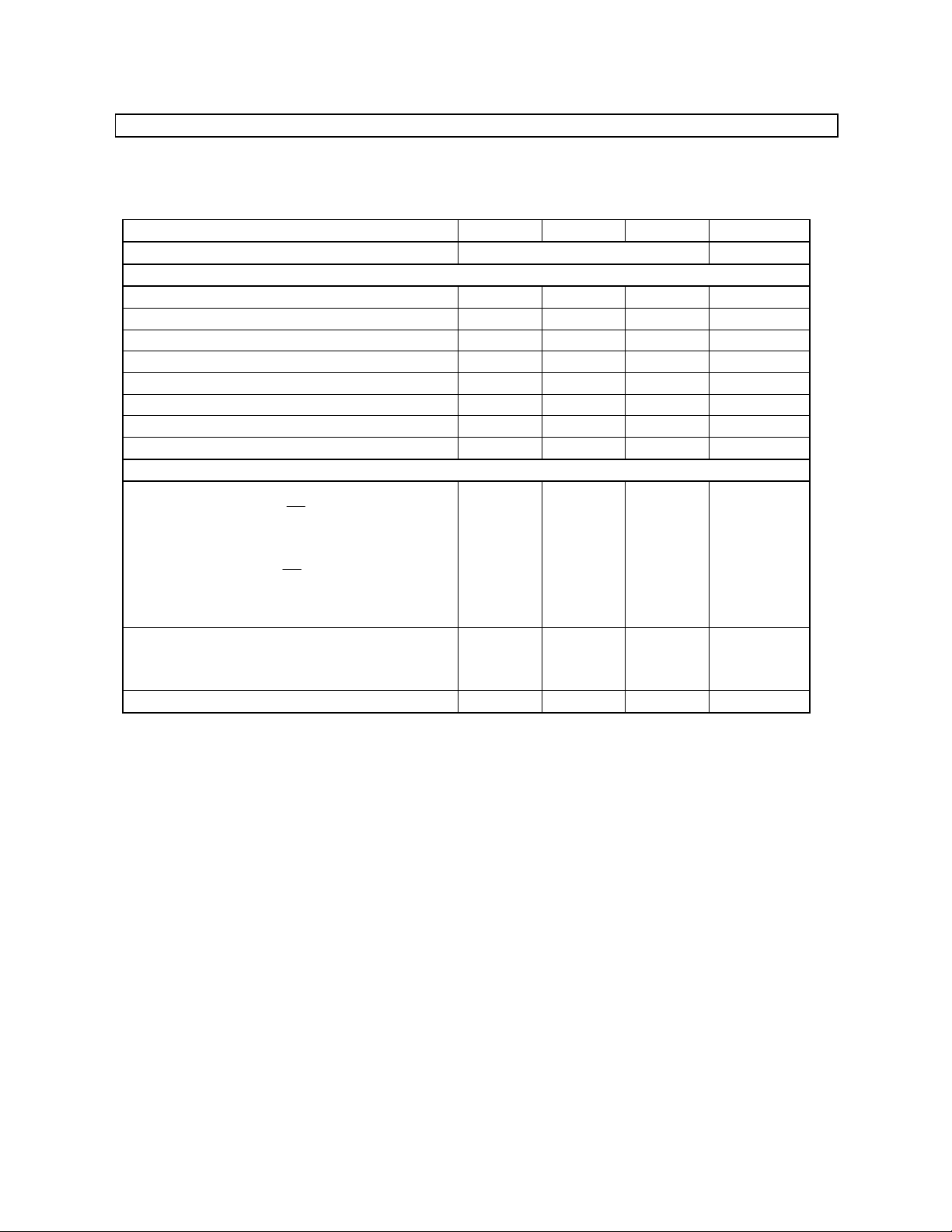
ANALOG CHARACTERISTICS
(Ta=25°C; VA,VD,VB=5.0V; fs=48kHz; 20bit; Input signal frequency=1kHz,
Measurement Bandwidth=10Hz~20kHz; unless otherwise specified.)
Parameter min typ max Units
Resolution 20 Bits
Analog Input Characteristics (Analog source impedance: 330Ω)
S/(N+D) (Note 4 ) 88 97 dB
Dynamic Range (A-weighted) (Note 5 ) 97 103 dB
S/N (A-weighted) (Note 6 ) 97 103 dB
Interchannel Isolation (f=1kHz) 100 120 dB
Interchannel Gain Mismatch 0.1 0.3 dB
200
Gain drift
Input Voltage Range
±
1.97
±
±
2.10
Input Impedance 30 50
±
2.23
ppm/°C
Vp-p
Ω
k
Power Supplies
Power Supply Current (Note 7 )
Normal Operation (PD="H")
VA+VB
VD
15
25
6
9
mA
mA
Power-Down mode (PD="L")
VA+VB
VD
20
10
uA
uA
Power Consumption (Note 7 )
Normal Operation
Power-Down mode
105
150
170 mW
uW
Power Supply Rejection Ratio 50 dB
Note 4 : The ratio of the rms value of the signal to the sum of all other spectral components up to 20kHz
except for the signal (included harmonic component, excluded DC component, analog input
signal is -0.5dB). Inversed of THD+N.
Note 5 : S/(N+D) with an input signal of 60dB below full-scale.
Note 6 : When using only 20kHzLPF, S/N and DR are 99dB(typ.). When using CCIR-AR M filt er,
S/N is 99dB(typ.)
Note 7 : Almost no current is supplied from VB pin.
0166-E-00 1997/4
- 6 -
 Loading...