

AKM AK4528 Datasheet
ASAHI KASEI [AK4528]
AK4528
High Performance 24Bit 96kHz Audio CODEC
GENERAL DESCRIPTIO N
The AK4528 is a high performance 24bit CODEC for the 96kHz recording system. The ADC has an
Enhanced Dual Bit architecture with wide dynamic range. The DAC uses the new developed Advanced
Multi Bit architecture and achieves low outband noise and high jitter tolerance by use of SCF (switched
capacitor filter) techniques.
FEATURES
· 24bit 2ch ADC
- 64x Oversampling
- Full differentia l Inputs
- S/(N+D): 94dB
- Dynamic Range, S/N: 108dB
- Digital HPF for offset cancellation
- I/F format: MSB justified or I
· 24bit 2ch DAC
- 128x Oversampling
- 24bit 8 times Digital Filter
Ripple: ±0.005dB, A ttenuati on: 75dB
- SCF
- Differential Outputs
- S/(N+D): 94dB
- Dynamic Range, S/N: 110dB
- De-emphasis for 32kHz, 44.1kHz and 48kHz sampling
- Output DATT with –72dB att
- Soft Mute
- I/F format: MSB justified, LSB justified or I
· High Jitter Tolerance
· 3-wire Serial Interface for Volume Control
· Master Clock
- 256fs/384fs/512fs/768fs/1024fs
· 5V operation
· 3V Power Supply Pin for 3V I/F
· Small 28pin VSOP package
2
S
2
S
MS0011-E-00 2000/1
- 1 -
ASAHI KASEI [AK4528]
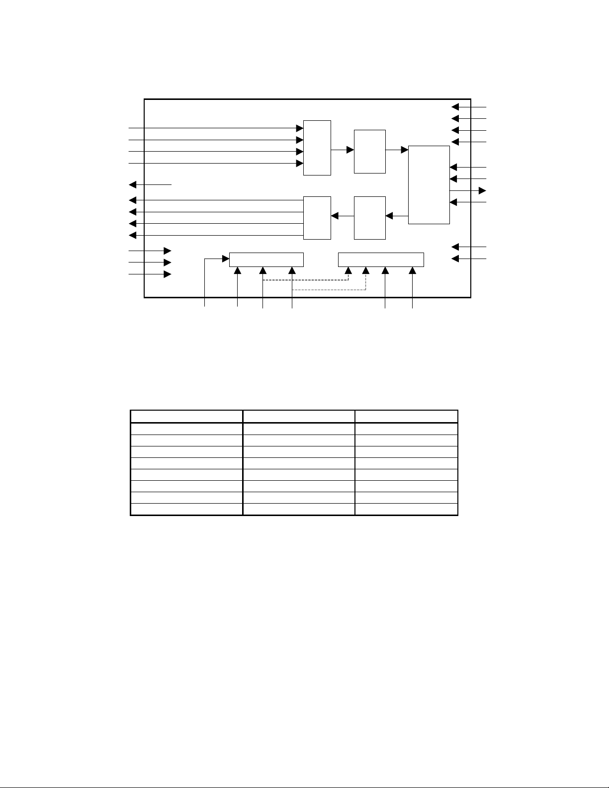
n Block Diagram
VD
AINL+
AINLAINR+
AINR-
VCOM
AOUTL+
AOUTLAOUTR+
AOUTR-
VREF
VA
AGND
ADC
DAC
Control Register I/F Clock Divider
HPF
DATT
SMUTE
Audio I/F
Controller
VT
DGND
PDN
LRCK
BICK
SDTO
SDTI
DEM0
DEM1
P/S
CSN
(DIF)
CCLK
(CKS1)
CDTI
(CKS0)
Block Diagram
· Compatibility of AK4528 with AK4524
Function AK4528 AK4524
ADC S/(N+D) 94dB 90dB
ADC DR, S/N 108dB 100dB
Input PGA & ATT X O
ADC Inputs Differential Inputs Single-end Inputs
Master Mode X O
X’tal Oscillating Circuit X O
Quad Speed Mode X O
Parallel Mode O X
O: Available, X: Not Available
MCLK
DFS
MS0011-E-00 2000/1
- 2 -
ASAHI KASEI [AK4528]
n Ordering Guide
AK4528VF -40~+85°C 28pin VSOP (0.65mm pitch)
AKD4528 Evaluation Board
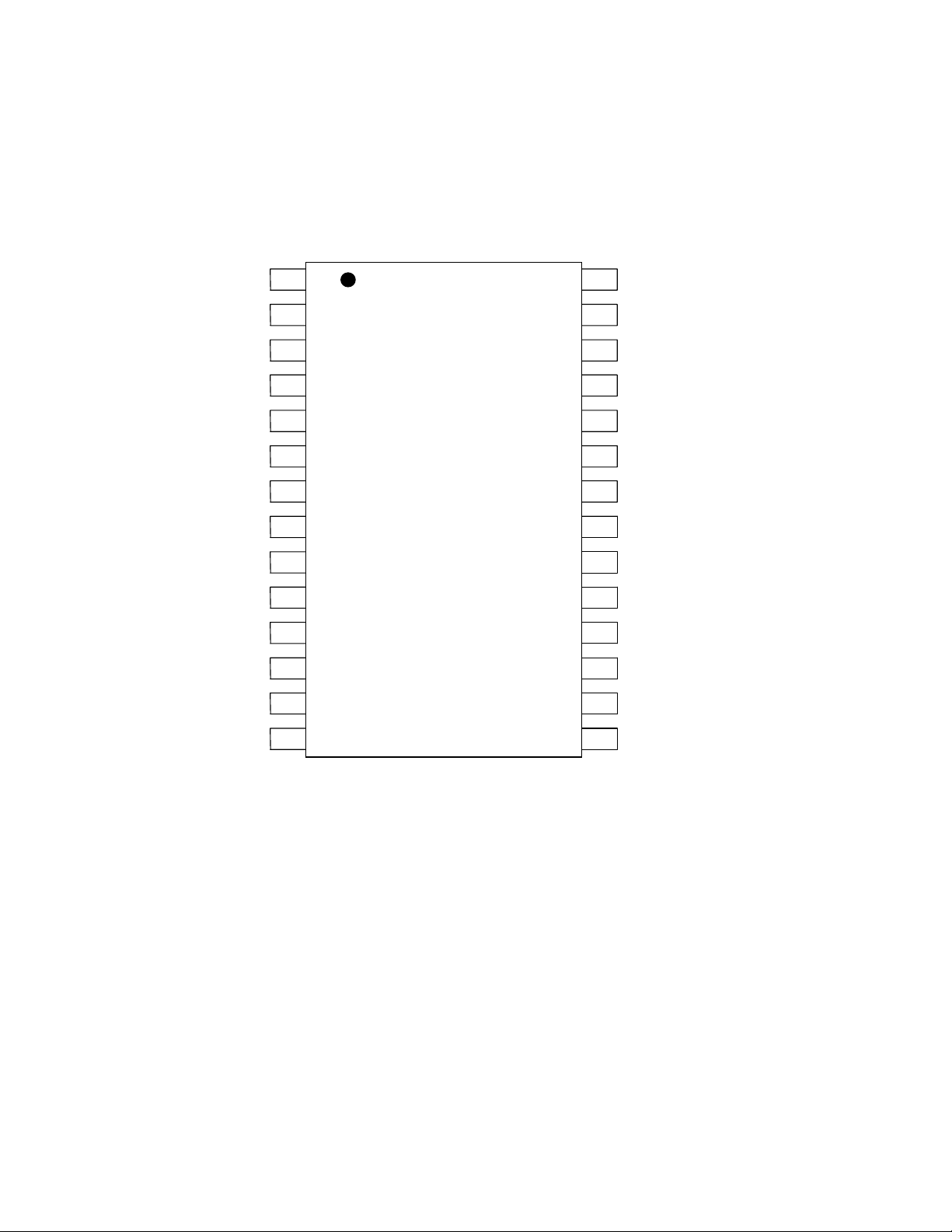
n Pin Layout
VCOM
AINR+
AINR-
AINL+
AINL-
VREF
AGND
VA
P/S
MCLK
LRCK
BICK
SDTO
1
2
3
4
5
6
7
8
9
10
11
12
13
AK4528
Top
View
28
27
26
25
24
23
22
21
20
19
18
17
16
AOUTR+
AOUTR-
AOUTL+
AOUTL-
DGND
VD
VT
DEM1
DEM0
PDN
DFS
CSN(DIF)
CCLK(CKS1)
SDTI CDTI(CKS0)
14 15
MS0011-E-00 2000/1
- 3 -
ASAHI KASEI [AK4528]
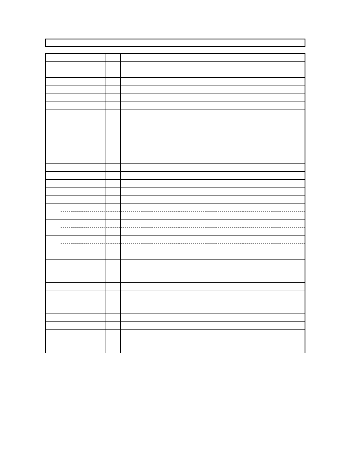
PIN/FUNCTION
No. Pin Name I/O Function
1VCOM O
Common Voltage Output Pin, VA/2
Bias voltage of ADC inputs and DAC outputs.
2 AINR+ I Rch Positive Input Pin
3 AINR- I Rch Negative Input Pin
4 AINL+ I Lch Positive Input Pin
5 AINL- I Lch Negative Input Pin
Voltage Reference Input Pin, VA
6VREF I
Used as a voltage reference by ADC & DAC. VREF is connected externally to
filtered VA.
7 AGND - Analog Gro und Pin
8 VA - Analog Power Supply Pin, 4.75 ~ 5.25V
9P/S I
Parallel/Serial Mode Select Pin
“L”: Serial Mode, “H”: Parallel Mode
10 MCLK I Master Clock Input Pin
11 LRCK I Inp ut/Output Channel Clock Pin
12 BICK I Audio Serial Data Clock Pin
13 SDTO O Audio Serial Data Output Pin
14 SDTI I Audio Serial Data Input Pin
CDTI I Control Data Input Pin in Serial Mode
15
CKS0 I Master Clock Select Pin
CCLK I Control Data Clock P in in Serial Mode
16
CKS1 I Master Clock Select Pin
CSN I Chip Select Pin in Serial Mode
17
DIF I
Digital Audio Interface Select Pin
“L”: 24bit MSB justified, “H”: I
2
S compatible
18 DFS I Double Speed Sampling Mode Pin
19 PDN I
Power-Down M ode Pin
“H”: Power up, “L”: Power down reset and initialize the control register.
20 DEM0 I De-emphasis Control Pin
21 DEM1 I De-emphasis Control Pin
22 VT - Output Buffer Power Supply Pin, 2.7 ~ 5.25V
23 VD - Digital Power Supply Pin, 4.75 ~ 5.25V
24 DGND - Digital Ground Pin
25 AOUTL- O Lch Negative Analog Output Pin
26 AOUTL+ O Lch Positive Analog Output Pin
27 AOUTR- O Rch Negative Analog Output Pin
28 AOUTR+ O Rch Positive Analog Output Pin
Note: All input pins should not be left floating.
MS0011-E-00 2000/1
- 4 -
ASAHI KASEI [AK4528]
ABSOLUTE MAXI MUM RATINGS
(AGND, DGND=0V; Note 1)
Parameter Symbol min max Units
Power Supplies: Analog
Digital
Output Buffer
VD-VA
Input Current, Any Pin Except Supplies IIN Analog Input Voltage VINA -0.3 VA+0.3 V
Digital Input Voltage VIND -0.3 VA+0.3 V
Ambient Temperature (powered applied) Ta -40 85
Storage Temperature Tstg -65 150
Note: 1. All voltages with respect to ground.
WARNING: Operation at or beyond these limits may result in permanent damage to the device.
Normal operation is not guaranteed at these extremes.
VA
VD
VT
VDA
-0.3
-0.3
-0.3
-
6.0
6.0
6.0
0.3
10 mA
±
V
V
V
V
C
°
C
°
RECOMMENDED OPERATING CONDITIONS
(AGND, DGND=0V; Note 1)
Parameter Symbol min typ max Units
Power Supplies Analog
Digital
Output Buffer
Voltage Reference VREF 3.0 - VA V
VA
VD
VT
4.75
4.75
2.7
5.0
5.0
3.0
5.25
VA
VD
V
V
V
Note:1. All voltages with respect to ground.
2. VA and VD should be powered at the same time or VA should be powered earlier than VD.
The power up sequence between VA and VT, or VD and VT is not critical.
*AKM assumes no responsibility for the usage beyond the conditions in this datasheet.
MS0011-E-00 2000/1
- 5 -

ASAHI KASEI [AK4528]
ANALOG CHARA CTERISTICS
(Ta=25°C; VA, VD, VT=5.0V; AGND=DGND=0V; VREF=VA; fs=44.1kHz; Signal Frequency =1kHz; 24bit Data;
Measurement frequency = 20Hz ~ 20kHz at fs=44.1kHz, 40Hz ~ 40kHz at fs=96kHz; unless otherwise specified)
Parameter min typ max Units
Input PGA Characteristics:
ADC Analog Input Characteristics: Analog Source impedance = 330
Resolution 24 Bits
Input Voltage (Note 3) ±2.6 ±2.8 ±3.0 Vpp
Input Resistance
S/(N+D) (-0.5dBFS) fs=44.1kHz
DR (-60dBFS) fs=44.1kHz, A-weighted
S/N fs=44.1kHz, A-weighted
Interchannel Isolation 90 110 dB
Interchannel Gain Mismatch 0.2 0.5 dB
Gain Drift 20 - ppm/°C
Input Voltage (Note 3) ±2.6 ±2.8 ±3.0 Vpp
Input Resistance
Input DC Bias Voltage (Note 4) 0.56VA - 0.60VA V
Power Supply Rejection (Note 5) - 50 - dB
DAC Analog Output Characteristics:
Resolution 24 Bits
S/(N+D) (0dBFS) fs=44.1kHz
DR (-60dBFS) fs=44.1kHz, A-weighted
S/N fs=44.1kHz, A-weighted
Interchannel Isolation 90 110 dB
Interchannel Gain Mismatch 0.2 0.5 dB
Gain Drift 20 - ppm/°C
Output Voltage (Note 6) 5.0 5.4 5.8 Vpp
Load Resistance (In case of AC load) 1 k
Output Current 1.5 mA
Load Capacitance 25 pF
Power Supply Rejection (Note 5) 50 - dB
fs=44.1kHz
fs=96kHz
fs=96kHz
fs=96kHz
fs=96kHz
fs=44.1kHz
fs=96kHz
fs=96kHz
fs=96kHz
fs=96kHz
16
7
88
84
100
95
100
95
16
7
88
85
104
96
104
96
WWWW
27
12
94
92
108
103
108
103
27
12
94
93
110
104
110
104
k
k
dB
dB
dB
dB
dB
dB
k
k
dB
dB
dB
dB
dB
dB
W
W
W
W
W
Note: 3. This voltage is input to AIN+ and AIN- pin, and is proportional to VREF. Vin = 0.56 x VREF.
4. Measured by Figure 12. DC Bias Voltage, Vb = 4.7k / (3.3k + 4.7k) x VA = 0.5875VA.
5. PSR is applied to VA, VD, VT with 1kHz, 50mVpp. VREF pin is held a constant voltage.
6. Full scale (0dB) of the output voltage when summing the differential outputs, AOUT+/- by unity gain.
This voltage is proportional to VREF. Vout=1.08 x VREF x Gain.
MS0011-E-00 2000/1
- 6 -
ASAHI KASEI [AK4528]
Parameter min typ max Units
Power Supplies
Power Supply Current
Normal Operation (PDN=“H”)
VA
VD+VT (fs=44.1kHz)
(fs=96kHz)
Power-down mode (PDN=“L”) (Note 7)
VA
VD+VT
Note: 7. All digital input pins are held VD or DGND.
38
10
18
10
10
57
20
36
100
100
mA
mA
mA
m
m
A
A
FILTER CHARACTERISTICS
(Ta=25°C; VA, VD=4.75 ~ 5.25V; VT=2.7 ~ 5.25V; fs=44.1kHz; DEM=OFF)
Parameter Symbol min typ max Units
ADC Digital Filter (Decimation LPF):
Passband (Note 8) -0.005dB
-0.02dB
-0.06dB
-6.0dB
Stopband SB 24.34 kHz
Passband Ripple PR
Stopband Attenuation SA 80 dB
Group Delay (Note 9) GD 31 1/fs
Group Delay Distortion
ADC Digital Filter (HPF):
Frequency Response (Note 8) -3dB
-0.5dB
-0.1dB
DAC Digital Filter:
Passband (Note 8) -0.01dB
-6.0dB
Stopband SB 24.1 kHz
Passband Ripple PR
Stopband Attenuation SA 75 dB
Group Delay (Note 9) GD 30 1/fs
DAC Digital Filter + SCF:
Frequency Response:
0 ~ 20.0kHz
~ 40kHz (Note 10)
PB 0
-
-
-
GD 0 us
D
FR 0.9
PB 0
- 22.05
FR
20.02
22.20
22.05
2.7
6.0
0.2
±
0.3
±
19.76
-
-
-
0.005 dB
±
20.0
-
0.005 dB
±
kHz
kHz
kHz
kHz
Hz
Hz
Hz
kHz
kHz
dB
dB
Note: 8. The passband and stopband frequencies scale with fs.
For example, 20.02kHz at -0.02dB is 0.454 x fs. The reference frequency of these responses is 1kHz.
9. The calculating delay time which occurred by digital filtering. This time is from the input of analog signal to
setting the 24bit data of both channels to the output register for ADC.
For DAC, this time is from setting the 24bit data of both channels on input register to the output of analog signal.
10. fs=96kHz.
MS0011-E-00 2000/1
- 7 -
ASAHI KASEI [AK4528]
DC CHARACTERISTICS
(Ta=25°C; VA,VD=4.75 ~ 5.25V; VT=2.7 ~ 5.25V)
Parameter Symbol min typ max Units
High-Level Input Voltage
Low-Level Input Voltage
High-Level Output Voltage (Iout=-100mA) (Note 11)
Low-Level Output Voltage (Iout=100mA)
Input Leakage Current Iin - -
VIH
VIL
VOH
VOL
2.2
-
2.7 / VT-0.5
-
-
-
-
-
-
0.8
-
0.5
10 µA
±
V
V
V
V
Note: 11. The min value is lower voltage of 2.7V or VT-0.5V.
SWITCHING CHARACTERISTICS
(Ta=25°C; VA,VD=4.75 ~ 5.25V, VT=2.7 ~ 5.25V; CL=20pF)
Parameter Symbol min typ max Units
Master Clock Timing
Frequency
Pulse Width Low
Pulse Width High
fCLK
tCLKL
tCLKH
7.68
0.4/fCLK
0.4/fCLK
55.296 MHz
ns
ns
LRCK Frequency
Normal Speed Mode (DFS = ”0”)
Double Speed Mode (DFS = ”1”)
Duty Cycle
fsn
fsd
Duty
30
60
45
44.1
88.2
54
108
55
kHz
kHz
%
Audio Interface Timing
BICK Period
BICK Pulse Width Low
Pulse Width High
LRCK Edge to BICK “” (Note 12)
BICK “” to LRCK Edge (Note 12)
2
LRCK to SDTO (MSB) (Except I
S mode)
BICK “¯” to SDTO
SDTI Hold Time
SDTI Setup Time
tBCK
tBCKL
tBCKH
tLRB
tBLR
tLRS
tBSD
tSDH
tSDS
81
33
33
20
20
20
20
Note 12. BICK rising edge must not occur at the same time as LRCK edge.
40
40
ns
ns
ns
ns
ns
ns
ns
ns
ns
MS0011-E-00 2000/1
- 8 -
ASAHI KASEI [AK4528]
Parameter Symbol min typ max Units
Control Interface Timing (P/S=“L”)
CCLK Period
CCLK Pulse Width Low
Pulse Width High
CDTI Setup Time
CDTI Hold Time
CSN “H” Time
CSN “L” Time
CSN “” to CCLK “”
CCLK “” to CSN “”
tCCK
tCCKL
tCCKH
tCDS
tCDH
tCSW
tCSW
tCSS
tCSH
200
80
80
40
40
150
150
150
50
ns
ns
ns
ns
ns
ns
ns
ns
ns
Reset Timing
PDN Pulse Width (Note 13)
RSTADN “” to SDTO valid (Note 14)
PDN “” to SDTO valid (Note 15)
tPD
tPDV
tPDV
150
516
516
ns
1/fs
1/fs
Note:13. The AK4528 can be reset by bringing PDN “L”.
14. In serial mode, these cycles are the number of LRCK rising from RSTADN bit.
15. In parallel mode, these cycles are the number of LRCK rising from PDN pin.
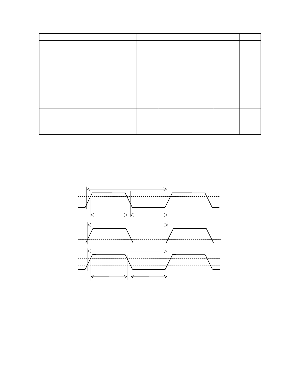
n Timing Diagram
MCLK
LRCK
BICK
tCLKH
tBCKH
1/fCLK
VIH
VIL
tCLKL
1/fs
VIH
VIL
tBCK
VIH
VIL
tBCKL
Clock Timing
MS0011-E-00 2000/1
- 9 -
 Loading...