

AKM AK4527B Datasheet
ASAHI KASEI [AK4527B]
AK4527B
High Performance Multi-channel Audio CODEC
GENERAL DESCRIPTION
The AK4527B is a single chip CODEC that includes two channels of ADC and six channels of DAC. The
ADC outputs 24bit data and the DAC accepts up to 24bit input data. The ADC has the Enhanced Dual Bit
architecture with wide dynamic range. The DAC introduces the new developed Advanced Multi-Bit
architecture, and achieves wider dynamic range and lower outband noise. An auxiliary digital audio input
interface maybe used instead of the ADC for passing audio data to the primary audio output port. Control
may be set directly by pins or programmed through a separate serial interface.
The AK4527B has a dynamic range of 102dB for ADC, 106dB for DAC and is well suited for digital
surround for home theater and car audio. An AC-3 system can be built with a IEC60958(SPDIF) receiver
such as the AK4112A. The AK4527B is available in a small 44pin LQFP package which will reduce
system space.
*AC-3 is a trademark of Dolby Laboratories.
FEATURES
o 2ch 24bit ADC
- 64x Oversampling
- Sampling Rate up to 96kHz
- Linear Phase Digital Anti-Alias Filter
- Differential Inputs with single-ended use capability
- S/(N+D): 92dB
- Dynamic Range, S/N: 102dB
- Digital HPF for offset cancellation
- I/F format: MSB justified or I
- Overflow flag
o 6ch 24bit DAC
- 128x Oversampling
- Sampling Rate up to 96kHz
- 24bit 8 times Digital Filter
- Single-Ended Outputs
- On-chip Switched-Capacitor Filter
- S/(N+D): 90dB
- Dynamic Range, S/N: 106dB
- I/F format: MSB justified, LSB justified(20bit,24bit) or I
- Individual channel digital volume with 256 levels and 0.5dB step
- Soft mute
- De-emphasis for 32kHz, 44.1kHz and 48kHz
- Zero Detect Function
o High Jitter Tolerance
o TTL Level Digital I/F
o 3-wire Serial and I
2
C Bus µP I/F for mode setting
o Master clock:256fs, 384fs or 512fs for fs=32kHz to 48kHz
128fs, 192fs or 256fs for fs=64kHz to 96kHz
o Power Supply: 4.5 to 5.5V
o Power Supply for output buffer: 2.7 to 5.5V
o Small 44pin LQFP
2
S
2
S
MS0056-E-00 2000/10
- 1 -
ASAHI KASEI [AK4527B]
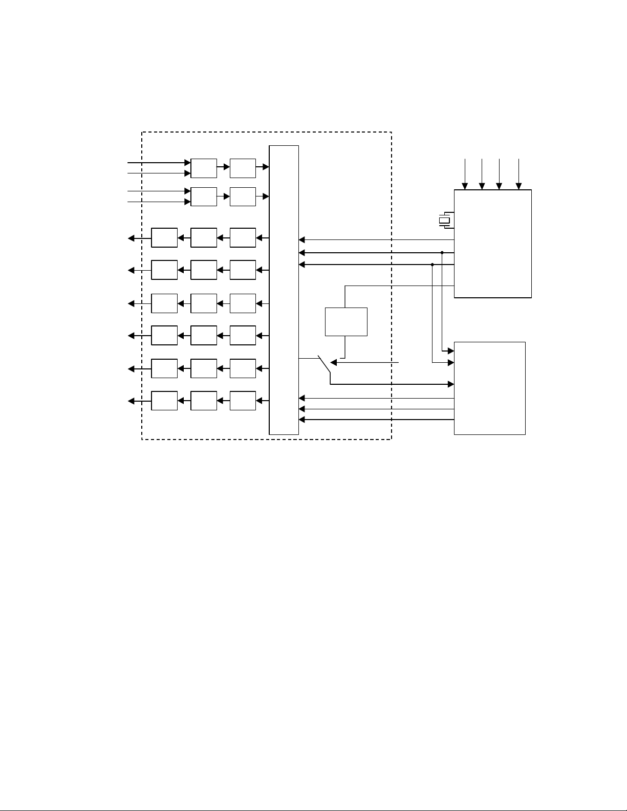
n Block Diagram
LIN+
LIN-
RIN+
RIN-
LOUT1
ROUT1
LOUT2
ROUT2
LOUT3
ROUT3
ADC
ADC
LPF
DAC
LPF DAC
LPF DAC
LPF DAC
LPF DAC
LPF DAC
AK4527B
HPF
HPF
DATT
DATT
DATT
DATT
DATT
DATT
Audio
I/F
MCLK
LRCK
BICK
SDOUT
SDIN1
SDIN2
SDIN3
Format
Converter
MCLK
LRCK
BICK
DAUX
SDOS
SDTO
SDTI1
SDTI2
SDTI3
XTI
XTO
MCKO
LRCK
BICK
SDTO
LRCK
BICK
SDIN
SDOUT1
SDOUT2
SDOUT3
RX4RX3RX2RX1
DIR
AK4112A
AC3
Block Diagram (DIR and AC-3 DSP are external parts)
MS0056-E-00 2000/10
- 2 -
ASAHI KASEI [AK4527B]
4
3
42
0
39
38
37
34
16
n Ordering Guide
AK4527BVQ -40 ∼ +85°C 44pin LQFP(0.8mm pitch)
AKD4527B Evaluation Board for AK4527B
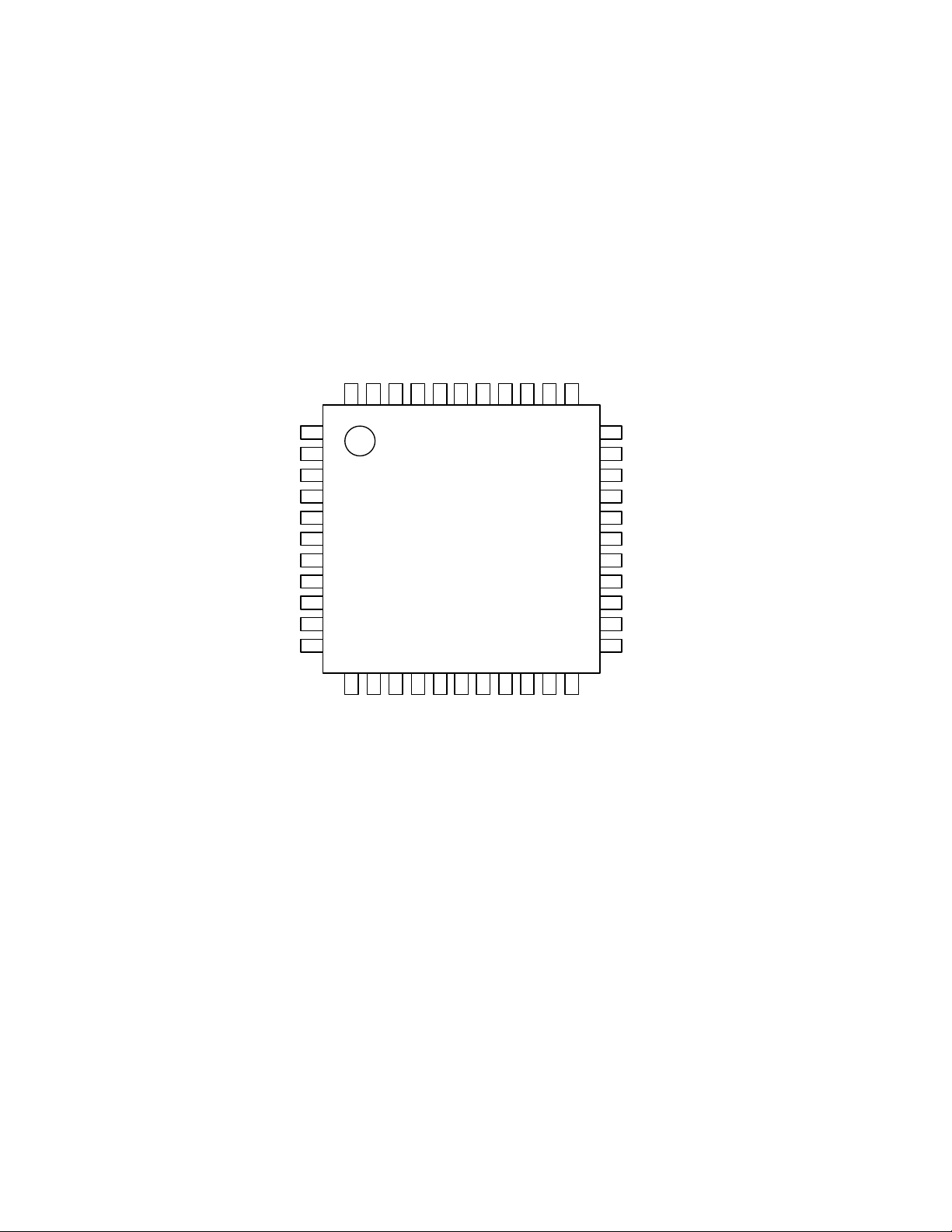
n Pin Layout
LOOP1
LOOP0/SDA/CDTI
DIF0/CSN
P/S
DIF1/SCL/CCLK
MCLK
DZF1
AVSS
AVDD36VREFH35VCOM
DOS
I2C
MUTE 3
ICK 4
RCK 5
DTI1 6
DTI2 7
DTI3 8
DTO 9
AUX 10
FS 11
4
1
2
4
AK4527BVQ
NC12DZFE13TVDD14DVDD15DVSS
41
4
Top View
17
PDN
33
32
31
30
29
28
27
26
25
24
23
22
TST18NC19ADIF20CAD121CAD0
DZF2/OVF
RIN+
RINLIN+
LINROUT1
LOUT1
ROUT2
LOUT2
ROUT3
LOUT3
MS0056-E-00 2000/10
- 3 -
ASAHI KASEI [AK4527B]
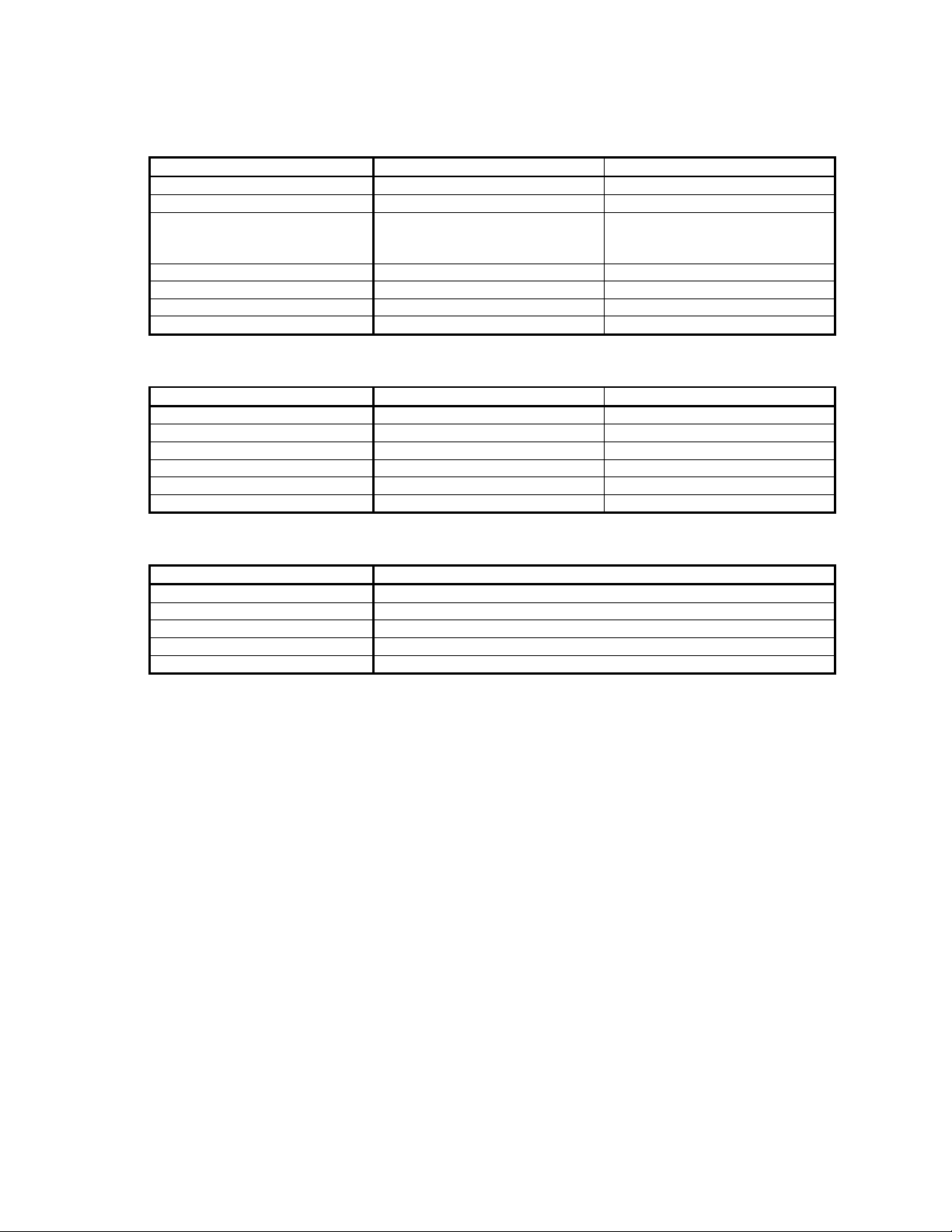
n Compatibility with AK4527
1. Functions
Functions AK4527 AK4527B
Overflow flag Not available Available
Clock mode Setting by pin/bit Auto setting
Sampling speed mode auto setting Not available Available
(MCLK is fixed at auto setting mode;
Normal: 512fs, Double: 256fs)
Zero detection Serial mode only Parallel/Serial mode
De-emphasis setting Pin/Register Register only
I2C bus mode Not available Available
Analog output at power down mode Hi-Z VCOM voltage
2. Pin Configuration
Pin# AK4527 AK4527B
12 DEM1 NC
13 DEM0 DZFE
18 ICKS2 TST
19 ICKS1 NC
20 ICKS0 ADIF
33 DZF2 DZF2/OVF
3. Register
Addr Changed items
00H DIF1-0 default values are changed from mode 0 to mode 2.
01H ACKS (Clock auto setting mode) is added.
08H DEMA1-C0 default values are changed from “44.1kHz” to “OFF”.
09H ICKS2-0 are removed.
0AH OVFE (Overflow detection enable) is added.
MS0056-E-00 2000/10
- 4 -
ASAHI KASEI [AK4527B]
PIN/FUNCTION
No. Pin Name I/O Function
1 SDOS I SDTO Source Select Pin (Note 1)
“L”: Internal ADC output, “H”: DAUX input
2 I2C I Control Mode Select Pin
“L”: 3-wire Serial, “H”: I
2
C Bus
3 SMUTE I Soft Mute Pin (Note 1)
When this pin goes to “H”, soft mute cycle is initialized.
When returning to “L”, the output mute releases.
4 BICK I Audio Serial Data Clock Pin
5 LRCK I Input Channel Clock Pin
6 SDTI1 I DAC1 Audio Serial Data Input Pin
7 SDTI2 I DAC2 Audio Serial Data Input Pin
8 SDTI3 I DAC3 Audio Serial Data Input Pin
9 SDTO O Audio Serial Data Output Pin
10 DAUX I AUX Audio Serial Data Input Pin
11 DFS I Double Speed Sampling Mode Pin (Note 1)
“L”: Normal Speed, “H”: Double Speed
12 NC - No Connect
No internal bonding.
13 DZFE I Zero Input Detect Enable Pin
“L”: mode 7 (disable) at parallel mode,
zero detect mode is selectable by DZFM2-0 bits at serial mode
“H”: mode 0 (DZF1 is AND of all six channels)
14 TVDD 15 DVDD -
Output Buffer Power Supply Pin, 2.7V∼5.5V
Digital Power Supply Pin, 4.5V∼5.5V
16 DVSS - Digital Ground Pin, 0V
17 PDN I Power-Down & Reset Pin
When “L”, the AK4527B is powered-down and the control registers are reset to default
state. If the state of P/S or CAD0-1 changes, then the AK4527B must be reset by PDN.
18 TST I Test Pin
This pin should be connected to DVSS.
19 NC - No Connect
No internal bonding.
20 ADIF I Analog Input Format Select Pin
“H”: Full-differential input, “L”: Single-ended input
21 CAD1 I Chip Address 1 Pin
22 CAD0 I Chip Address 0 Pin
MS0056-E-00 2000/10
- 5 -
ASAHI KASEI [AK4527B]
No. Pin Name I/O Function
23 LOUT3 O DAC3 Lch Analog Output Pin
24 ROUT3 O DAC3 Rch Analog Output Pin
25 LOUT2 O DAC2 Lch Analog Output Pin
26 ROUT2 O DAC2 Rch Analog Output Pin
27 LOUT1 O DAC1 Lch Analog Output Pin
28 ROUT1 O DAC1 Rch Analog Output Pin
29 LIN- I Lch Analog Negative Input Pin
30 LIN+ I Lch Analog Positive Input Pin
31 RIN- I Rch Analog Negative Input Pin
32 RIN+ I Rch Analog Positive Input Pin
DZF2 O Zero Input Detect 2 Pin (Note 2)
33
When the input data of the group 1 follow total 8192 LRCK cycles with “0” input data,
this pin goes to “H”.
OVF O Analog Input Overflow Detect Pin (Note 3)
This pin goes to “H” if the analog input of Lch or Rch is overflows.
34 VCOM O Common Voltage Output Pin, AVDD/2
Large external capacitor around 2.2µF is used to reduce power-supply noise.
35 VREFH I Positive Voltage Reference Input Pin, AVDD
36 AVDD -
Analog Power Supply Pin, 4.5V∼5.5V
37 AVSS - Analog Ground Pin, 0V
38 DZF1 O Zero Input Detect 1 Pin (Note 2)
When the input data of the group 1 follow total 8192 LRCK cycles with “0” input data,
this pin goes to “H”.
39 MCLK I Master Clock Input Pin
40 P/S I Parallel/Serial Select Pin
“L”: Serial control mode, “H”: Parallel control mode
DIF0 I Audio Data Interface Format 0 Pin in parallel control mode41
CSN I Chip Select Pin in 3-wire serial control mode
This pin should be connected to DVDD at I
2
C bus control mode
DIF1 I Audio Data Interface Format 1 Pin in parallel control mode42
SCL/CCLK I Control Data Clock Pin in serial control mode
I2C = “L”: CCLK (3-wire Serial), I2C = “H”: SCL (I
LOOP0 I Loopback Mode 0 Pin in parallel control mode
43
2
C Bus)
Enables digital loop-back from ADC to 3 DACs.
SDA/CDTI I/ O Control Data Input Pin in serial control mode
I2C = “L”: CDTI (3-wire Serial), I2C = “H”: SDA (I
2
C Bus)
44 LOOP1 I Loopback Mode 1 Pin (Note 1)
Enables all 3 DAC channels to be input from SDTI1.
Notes: 1. SDOS, SMUTE, DFS, and LOOP1 pins are ORed with register data if P/S = “L”.
2. The group 1 and 2 can be selected by DZFM2-0 bits if P/S = “L” and DZFE = “L”.
3. This pin becomes OVF pin if OVFE bit is set to “1” at serial control mode.
4. All input pins should not be left floating.
MS0056-E-00 2000/10
- 6 -

ASAHI KASEI [AK4527B]
ABSOLUTE MAXIMUM RATINGS
(AVSS, DVSS=0V; Note 5)
Parameter Symbol min max Units
Power Supplies Analog
Digital
Output buffer
|AVSS-DVSS| (Note 6)
Input Current (any pins except for supplies) IIN Analog Input Voltage VINA -0.3 AVDD+0.3 V
Digital Input Voltage VIND -0.3 DVDD+0.3 V
Ambient Temperature (power applied) Ta -40 85
Storage Temperature Tstg -65 150
Notes: 5. All voltages with respect to ground.
6. AVSS and DVSS must be connected to the same analog ground plane.
WARNING: Operation at or beyond these limits may result in permanent damage to the device.
Normal operation is not guaranteed at these extremes.
AVDD
DVDD
TVDD
∆GND
-0.3
-0.3
-0.3
-
6.0
6.0
6.0
0.3
±10
V
V
V
V
mA
°C
°C
RECOMMENDED OPERATING CONDITIONS
(AVSS, DVSS=0V; Note 5)
Parameter Symbol min typ max Units
Power Supplies
(Note 7)
Analog
Digital
Output buffer
AVDD
DVDD
TVDD
4.5
4.5
2.7
5.0
5.0
5.0
5.5
5.5
5.5
V
V
V
Notes: 5. All voltages with respect to ground.
7. The power up sequence between AVDD, DVDD and TVDD is not critical.
WARNING: AKM assumes no responsibility for the usage beyond the conditions in this datasheet.
MS0056-E-00 2000/10
- 7 -
ASAHI KASEI [AK4527B]
ANALOG CHARACTERISTICS
(Ta=25°C; AVDD, DVDD, TVDD=5V; AVSS, DVSS=0V; VREFH=AVDD; fs=44.1kHz; BICK=64fs;
Signal Frequency=1kHz; 24bit Data; Measurement Frequency=20Hz∼20kHz at fs=44.1kHz, 20Hz~40kHz at fs=96kHz;
unless otherwise specified)
Parameter min typ max Units
ADC Analog Input Characteristics: Differential Inputs; Analog Source Impedance=470Ω
Resolution 24 Bits
S/(N+D) (-0.5dBFS)
(Note 8)
DR (-60dBFS) fs=44.1kHz, A-weighted
S/N (Note 9) fs=44.1kHz, A-weighted
Interchannel Isolation 90 110 dB
DC Accuracy
Interchannel Gain Mismatch 0.2 0. 3 dB
Gain Drift 20 Input Voltage AIN=0.6xVREFH (Note 10) 2.85 3.0 3.15 Vpp
Input Resistance (Note 11) 18 28
Power Supply Rejection (Note 12) 50 dB
DAC Analog Output Characteristics:
Resolution 24 Bits
S/(N+D) fs=44.1kHz
DR (-60dBFS) fs=44.1kHz, A-weighted
S/N (Note 13) fs=44.1kHz, A-weighted
Interchannel Isolation 90 110 dB
DC Accuracy
Interchannel Gain Mismatch 0.2 0.5 dB
Gain Drift 20 Output Voltage AOUT=0.6xVREFH 2.75 3.0 3.25 Vpp
Load Resistance 5
Power Supply Rejection (Note 12) 50 dB
Power Supplies
Power Supply Current
Normal Operation (PDN = “H”)
AVDD
DVDD+TVDD fs=44.1kHz (Note 14)
fs=96kHz
Power-down mode (PDN = “L”) (Note 15)
Notes: 8. In case of single ended input, S/(N+D)=80dB(typ, @AVDD=5V, fs=44.1kHz).
9. S/N measured by CCIR-ARM is 98dB(@fs=44.1kHz).
10. Full scale input for each AIN+/- pin is 1.5Vpp in differential mode.
11. Input resistance is 14kΩ typically at fs=96kHz.
12. PSR is applied to AVDD, DVDD and TVDD with 1kHz, 50mVpp. VREFH pin is held a constant voltage.
13. S/N measured by CCIR-ARM is 102dB(@fs=44.1kHz).
14. DVDD=TBDmA, TVDD=TBDmA(typ).
15. In the power-down mode. All digital input pins including clock pins (MCLK, BICK, LRCK) are held DVSS.
fs=44.1kHz
fs=96kHz
fs=96kHz
fs=96kHz, A-weighted
fs=96kHz
fs=96kHz, A-weighted
fs=96kHz
fs=96kHz
fs=96kHz, A-weighted
fs=96kHz
fs=96kHz, A-weighted
84
94
88
93
94
88
93
80
78
95
88
94
95
88
94
92
-
83
102
96
102
102
96
102
90
88
106
100
106
106
100
106
35
25
35
80
56
40
56
200
dB
dB
dB
dB
dB
dB
dB
dB
ppm/°C
kΩ
dB
dB
dB
dB
dB
dB
dB
dB
ppm/°C
kΩ
mA
mA
mA
µA
MS0056-E-00 2000/10
- 8 -

ASAHI KASEI [AK4527B]
FILTER CHARACTERISTICS
(Ta=25°C; AVDD, DVDD=4.5∼5.5V; TVDD=2.7∼5.5V; fs=44.1kHz; DEM=OFF)
Parameter Symbol min typ max Units
ADC Digital Filter (Decimation LPF):
Passband (Note 16) -0.005dB
-0.02dB
-0.06dB
-6.0dB
Stopband SB 24.34 kHz
Passband Ripple PR
Stopband Attenuation SA 80 dB
Group Delay (Note 17) GD 27.6 1/fs
Group Delay Distortion
ADC Digital Filter (HPF):
Frequency Response (Note 16) -3dB
-0.5dB
-0.1dB
DAC Digital Filter:
Passband (Note 16) -0.1dB
-6.0dB
Stopband SB 24.2 kHz
Passband Ripple PR
Stopband Attenuation SA 56 dB
Group Delay (Note 17) GD 21.9 1/fs
DAC Digital Filter + Analog Filter:
Frequency Response: 0 ∼ 20.0kHz
40.0kHz (Note 18)
PB 0
-
-
-
∆GD
FR 0.9
PB 0
- 22.05
FR
FR
20.02
20.20
22.05
19.76
-
-
-
±0.005
0µs
2.7
6.0
20.0
-
±0.02
±0.2
±0.3
kHz
kHz
kHz
kHz
dB
Hz
Hz
Hz
kHz
kHz
dB
dB
dB
Notes: 16. The passband and stopband frequencies scale with fs.
For example, 20.02kHz at –0.02dB is 0.454 x fs. The reference frequency of these responses is 1kHz.
17. The calculating delay time which occurred by digital filtering. This time is from setting the input of analog
signal to setting the 24bit data of both channels to the output register for ADC.
For DAC, this time is from setting the 20/24bit data of both channels on input register to the output of analog
signal.
18. fs=96kHz.
MS0056-E-00 2000/10
- 9 -
ASAHI KASEI [AK4527B]
DC CHARACTERISTICS
(Ta=25°C; AVDD, DVDD=4.5∼5.5V; TVDD=2.7∼5.5V)
Parameter Symbol min typ max Units
High-Level Input Voltage
Low-Level Input Voltage
High-Level Output Voltage
(SDTO pin: Iout=-100µA)
(DZF1, DZF2/OZF pins: Iout=-100µA)
Low-Level Output Voltage
(SDTO, DZF1, DZF2/OZF pins: Iout= 100µA)
(SDA pin: Iout= 3mA)
Input Leakage Current Iin - - ±10 µA
VIH
VIL
VOH
VOH
VOL
VOL
2.2
-
TVDD-0.5
AVDD-0.5
-
-
-
-
-
-
-
-
0.8
0.5
0.4
-
-
-
V
V
V
V
V
V
SWITCHING CHARACTERISTICS
(Ta=25°C; AVDD, DVDD=4.5∼5.5V; TVDD=2.7∼5.5V; CL=20pF)
Parameter Symbol min typ max Units
Master Clock Input
256fsn, 128fsd:
Pulse Width Low
Pulse Width High
384fsn, 192fsd:
Pulse Width Low
Pulse Width High
512fsn, 256fsd:
Pulse Width Low
Pulse Width High
LRCK frequency
Normal Speed Mode
Double Speed Mode
Duty Cycle
Audio Interface Timing
BICK Period
BICK Pulse Width Low
Pulse Width High
LRCK Edge to BICK “↑” (Note 19)
BICK “↑” to LRCK Edge (Note 19)
LRCK to SDTO(MSB)
BICK “↓” to SDTO
SDTI1-3, DAUX Hold Time
SDTI1-3, DAUX Setup Time
fCLK
tCLKL
tCLKH
fCLK
tCLKL
tCLKH
fCLK
tCLKL
tCLKH
fsn
fsd
Duty
tBCK
tBCKL
tBCKH
tLRB
tBLR
tLRS
tBSD
tSDH
tSDS
8.192
27
27
12.288
20
20
16.384
15
15
32
64
45
160
65
65
45
45
40
25
12.288
18.432
24.576
48
96
55
40
40
MHz
ns
ns
MHz
ns
ns
MHz
ns
ns
kHz
kHz
%
ns
ns
ns
ns
ns
ns
ns
ns
ns
Notes: 19. BICK rising edge must not occur at the same time as LRCK edge.
MS0056-E-00 2000/10
- 10 -
 Loading...