

ASAHI KASEI [AK4522]
AK4522
20Bit Stereo ∆Σ ADC & DAC
GENERAL DESCRIPTION
The AK4522 has a dynamic range of 100dB and is well-suited middle-range MD, surround system,
musical instruments and car audio. Signal inputs and outputs are single-ended. The DAC outputs are
analog filtered to remove out of band noise. External components are minimized. The AK4522 is available
in a small 24pin VSOP package, which will reduce system space.
FEATURES
• ∆Σ Stereo ADC
- 64x Oversampling
- Sampling Rate Ranging from 16kHz to 48kHz
- S/(N+D): 92dB
- Dynamic Range, S/N: 100dB
- Digital HPF for offset cancellation
• ∆Σ Stereo DAC
- 128x Oversampling
- Sampling Rate Ranging from 16kHz to 48kHz
- 2nd order SCF + 2nd order CTF
- Digital de-emphasis for 32kHz, 44.1kHz, 48kHz sampling
- S/(N+D): 90dB
- Dynamic Range, S/N: 100dB
- Soft Mute
• High Jitter Tolerance
• Master Clock: 256fs, 384fs, 512fs
• Analog Power Supply: 4.5 to 5.5V, Digital Power Supply: 2.7 to 5.5V
• Small VSOP Package: 24pin VSOP
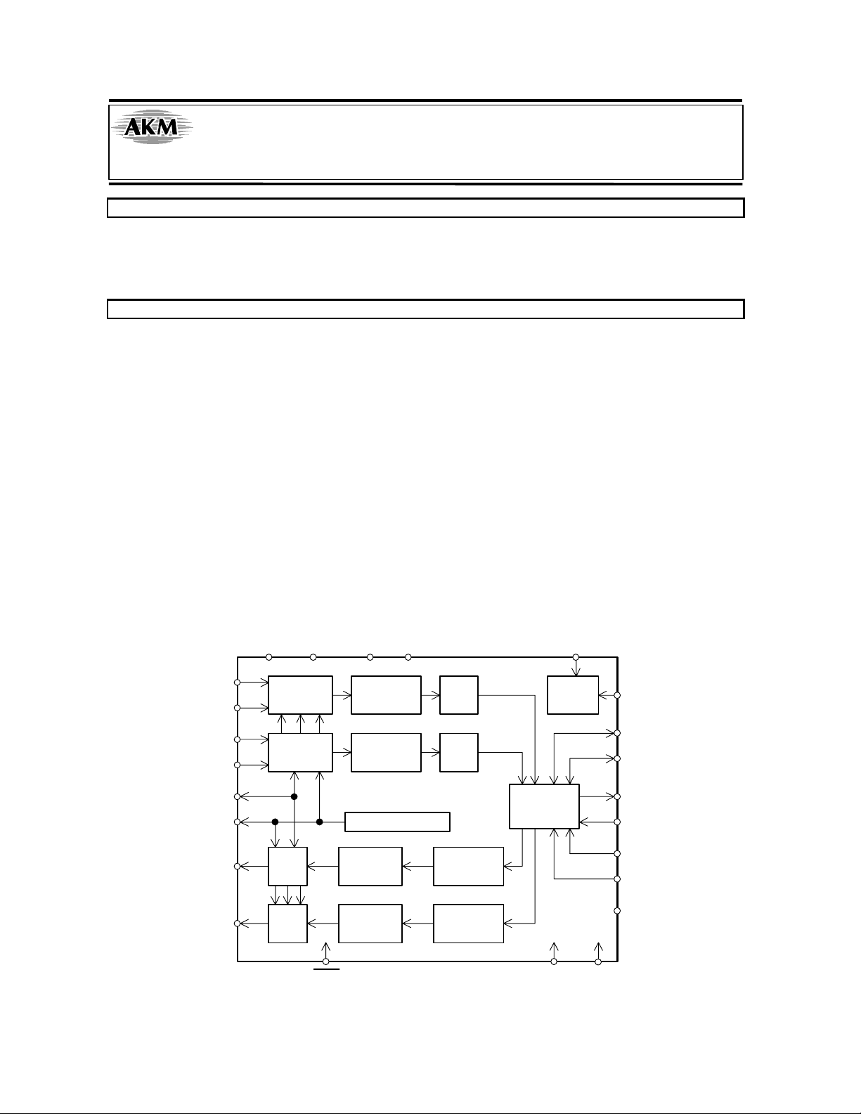
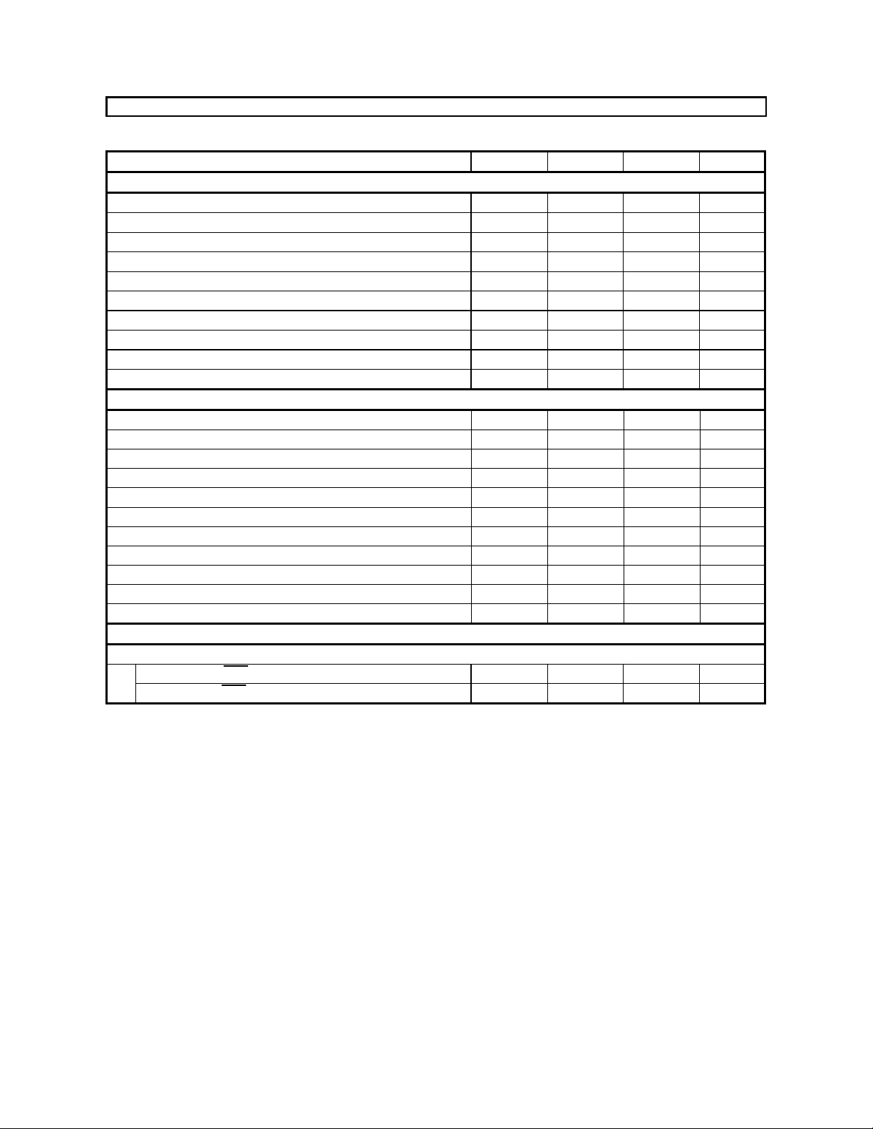
VA AGND VD DGND CMODE
AINL+
AINL-
AINR+
AINR-
VREFH
VCOM
AOUTL
AOUTR
M0020-E-01 1998/10
∆Σ
Modulator
∆Σ
Modulator
LPF
LPF
Decimation
Filter
Decimation
Filter
Common Voltage
∆Σ
Modulator
∆Σ
Modulator
PD
HPF
HPF
Interpolator
Interpolator
- 1 -
8x
8x
Clock
Divider
Serial I/O
Interface
MCKI
LRCK
SCLK
SDTO
SDTI
DIF0
DIF1
SMUTE
DEM1DEM0
ASAHI KASEI [AK4522]
n Ordering Guide
AK4522VF -10 ∼ +70°C 24pin VSOP (0.65mm pitch)
AKD4522 Evaluation Board for AK4522
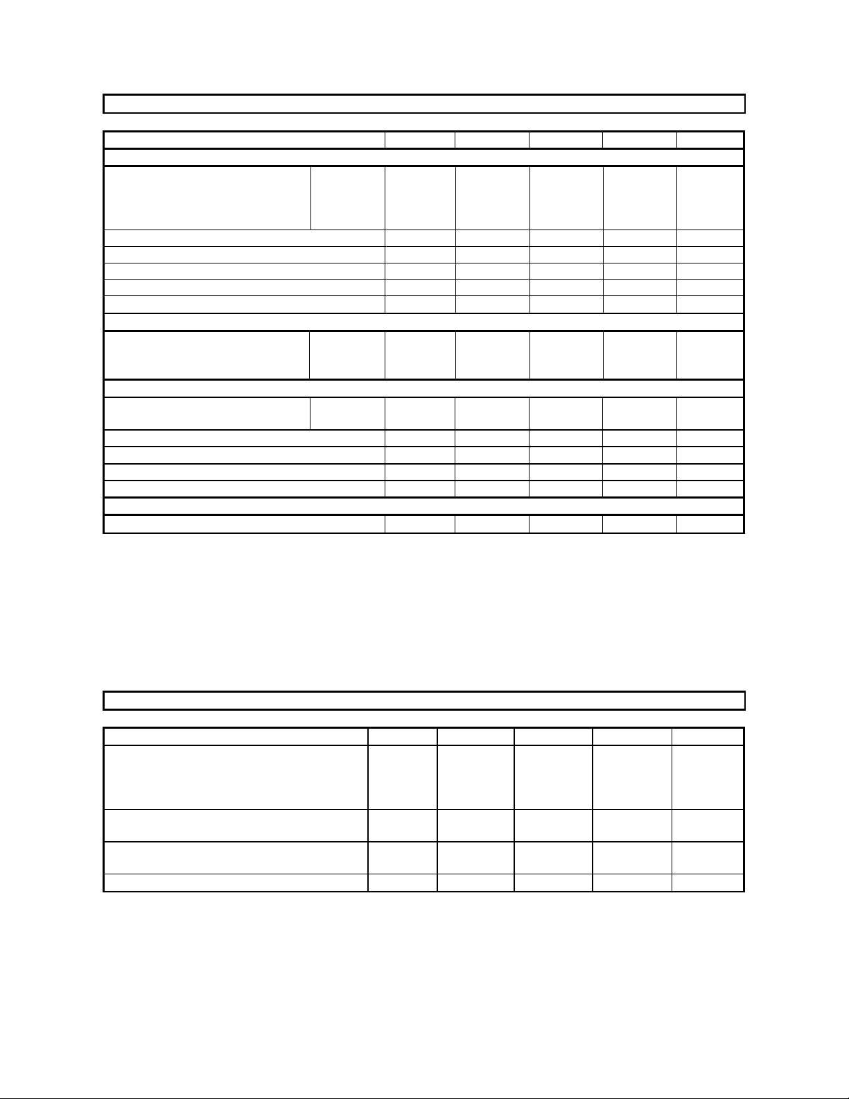
n Pin Layout
AINR+
AINR-
AINL+
AINL-
VA
AGND 7
DIF0 8
DIF1
LRCK
SCLK 11
SDTI 12
10
1VREFH
2
3
4
5
6
Top
View
9
24
23
22
21
20
19
18
17
16
15
14
13
VCOM
AOUTR
AOUTL
CMODE
PD
DGND
VD
MCKI
DEM1
DEM0
SMUTE
SDTO
M0020-E-01 1998/10
- 2 -
ASAHI KASEI [AK4522]
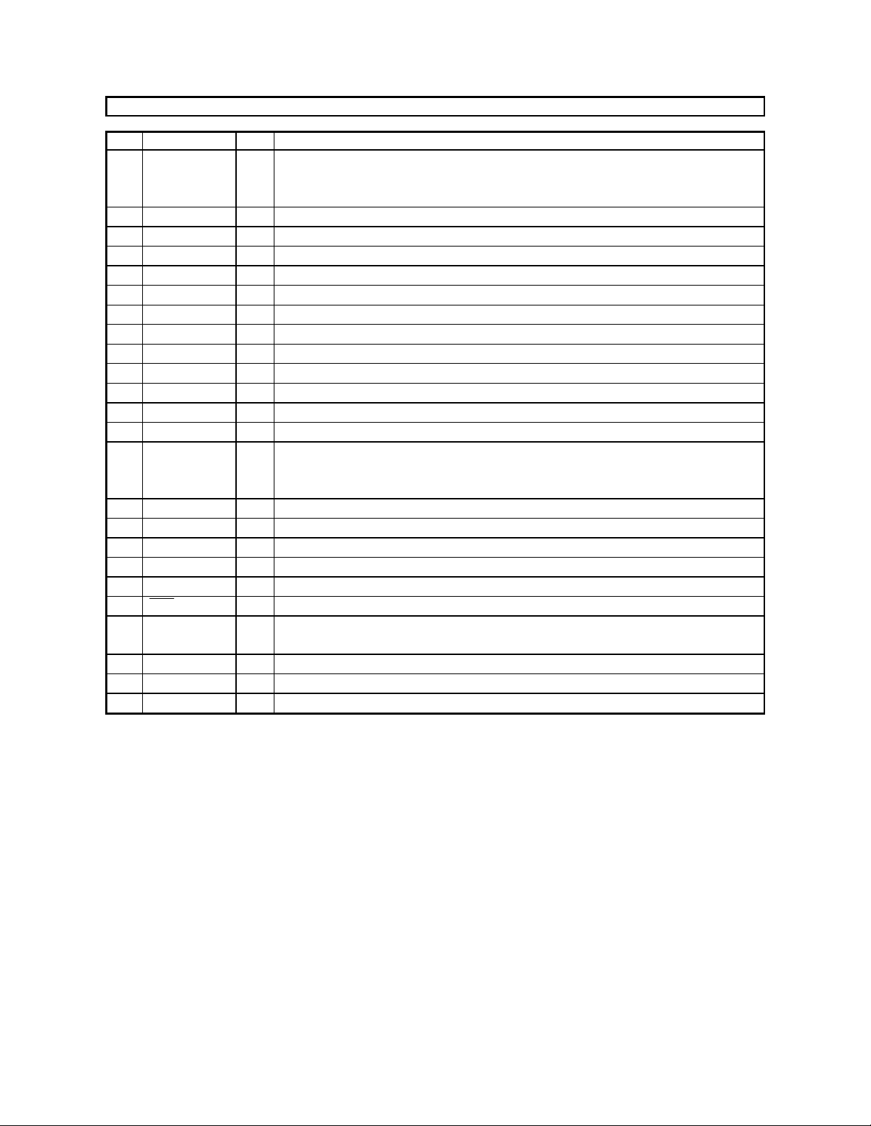
PIN/FUNCTION
No. Pin Name I/O Function
Positive Voltage Reference Input Pin, VA
1 VREFH I
2 AINR+ I Rch Analog Positive Input Pin
3 AINR- I Rch Analog Negative Input Pin
4 AINL+ I Lch Analog Positive Input Pin
5 AINL- I Lch Analog Negative Input Pin
6 VA - Analog Power Supply Pin
7 AGND - Analog Ground Pin
8 DIF0 I Audio Data Interface Format Pin
9 DIF1 I Audio Data Interface Format Pin
10 LRCK I Input/Output Channel Clock Pin
11 SCLK I Audio Serial Data Clock Pin
12 SDTI I Audio Serial Data Input Pin
13 SDTO O Audio Serial Data Output Pin
14 SMUTE I
15 DEM0 I De-emphasis Frequency Select Pin
16 DEM1 I De-emphasis Frequency Select Pin
17 MCKI I Master Clock Input/X’tal Input Pin
18 VD - Digital Power Supply Pin
19 DGND - Digital Ground Pin
20 PD I Reset Pin
21 CMODE I
22 AOUTL I Lch Analog Output Pin
23 AOUTR I Rch Analog Output Pin
24 VCOM O Common Voltage Output Pin, VA/2
Used as a positive voltage reference by ADC & DAC. VREFH should be connected
externally to filtered VA.
Soft Mute Pin
When this pin goes “H”, soft mute cycle is initiated.
When returning “L”, the output mute releases.
Master Clock Select Pin (Internal Biased pin)
“H”: 384fs, “L”: 256fs, “NC”: 512fs
Note: All input pins except pull-down pins should not be left floating.
M0020-E-01 1998/10
- 3 -
ASAHI KASEI [AK4522]
ABSOLUTE MAXIMUM RATINGS
(AGND DGND=0V; Note 1)
Parameter Symbol min max Units
Power Supplies Analog
Digital
|AGND-DGND| (Note 2)
Input Current, Any Pin Except Supplies IIN Analog Input Voltage VINA -0.3 VA+0.3 V
Digital Input Voltage VIND -0.3 VD+0.3 V
Ambient Temperature (power applied) Ta -10 70
Storage Temperature Tstg -65 150
Note:1. All voltages with respect to ground.
2. AGND and DGND must be same voltage.
WARNING: Operation at or beyond these limits may result in permanent damage to the device.
Normal operation is not guaranteed at these extremes.
VA
VD
∆GND
-0.3
-0.3
-
6.0
6.0
0.3
±10
V
V
V
mA
°C
°C
RECOMMENDED OPERATING CONDITIONS
(AGND, DGND=0V; Note 1)
Parameter Symbol min typ max Units
Power Supplies
(Note 3)
Analog
Digital
VA
VD
4.5
2.7
5.0
5.0
5.5
VA
V
V
Note:1. All voltages with respect to ground.
3. The power up sequence between VA and VD is not critical.
*AKM assumes no responsibility for the usage beyond the conditions in this datasheet.
M0020-E-01 1998/10
- 4 -
ASAHI KASEI [AK4522]
ANALOG CHARACTERISTICS
(Ta=25°C; VA, VD=5V; AGND, DGND=0V; VREFH=VA; fs=44.1kHz; SCLK=64fs;
Signal Frequency =1kHz; 20bit Data; Measurement Frequency=10Hz ∼ 20kHz; unless otherwise specified)
Parameter min typ max Units
ADC Analog Input Characteristics: Differential Inputs; Analog Source Impedance=470Ω
Resolution 20 Bits
S/(N+D) (-0.5dB Input) (Note 4) 84 92 dB
DR (-60dB Input, A-Weighted) (Note 5) 94 100 dB
S/N (A-Weighted) (Note 5, 6) 94 100 dB
Interchannel Isolation 90 110 dB
Interchannel Gain Mismatch 0.1 0.3 dB
Gain Drift 20 ppm/°C
Input Voltage (AIN=0.6 x VREFH) (Note 7) 2.85 3.0 3.15 Vpp
Input Resistance 20 30 kΩ
Power Supply Rejection (Note 8) 50 dB
DAC Analog Output Characteristics:
Resolution 20 Bits
S/(N+D) 80 90 dB
DR (-60dB Output, A-Weighted) (Note 5) 95 100 dB
S/N (A-Weighted) (Note 6, 9) 95 100 dB
Interchannel Isolation 90 110 dB
Interchannel Gain Mismatch 0.2 0.5 dB
Gain Drift 20 ppm/°C
Output Voltage (AOUT=0.6 x VREFH) 2.65 2.9 3.15 Vpp
Load Resistance 5 kΩ
Load Capacitance 25 pF
Power Supply Rejection (Note 8) 50 dB
Power Supplies
Power Supply Current (VA=VD=5V)
Analog, VA PD =”H” 42 55 m A
Digital, VD PD =”H” 10 20 mA
Note: 4. In case of single ended input, S/(N+D)=80dB(typ, @VA=5V).
5. In case of 16bit, DR and S/N of ADC are 98dB. DR of DAC is 98dB.
6. S/N measured by CCIR-ARM is 96dB at each converter and 94dB at ADC to DAC loopback.
7. Full scale input for each AIN+/- pin is 1.5Vpp in differential mode.
8. PSR is applied to VA, VD with 1kHz, 50mVpp. VREFH pin is held a constant voltage.
9. As the input data is “0”, S/N is 100dB regardless of resolution.
M0020-E-01 1998/10
- 5 -
ASAHI KASEI [AK4522]
FILTER CHARACTERISTICS
(Ta=25°C; VA=4.5 ∼ 5.5V, VD=2.7 ∼ 5.5V; fs=44.1kHz; DEM0=”1”, DEM1=”0”)
Parameter Symbol min typ max Units
ADC Digital Filter (Decimation LPF):
Passband (Note 10) -0.005dB
-0.02dB
-0.06dB
-6.0dB
Stopband SB 24.34 kHz
Passband Ripple PR
Stopband Attenuation SA 80 dB
Group Delay (Note 11) GD 29.3 1/fs
Group Delay Distortion
ADC Digital Filter (HPF):
Frequency Response (Note 10) -3dB
-0.5dB
-0.1dB
DAC Digital Filter:
Passband (Note 10) -0.06dB
-6.0dB
Stopband SB 24.1 kHz
Passband Ripple PR
Stopband Attenuation SA 43 dB
Group Delay (Note 11) GD 14.7 1/fs
DAC Digital Filter + Analog Filter:
Frequency Response: 0 ∼ 20.0kHz
PB 0
0
0
0
∆GD
FR 0.9
PB 0
0
FR
19.76
20.02
20.20
22.05
±0.005
0us
2.7
6.0
20.0
22.05
±0.06
±0.2
kHz
kHz
kHz
kHz
dB
Hz
Hz
Hz
kHz
kHz
dB
dB
Note:10. The passband and stopband frequencies scale with fs.
For example, 20.02kHz at -0.02dB is 0.454 x fs. The reference frequency of these responses is 1kHz.
11. The calculating delay time which occurred by digital filtering. This time is from the input of analog signal to
setting the 20bit data of both channels to the output register for ADC.
For DAC, this time is from setting the 20bit data of both channels on input register to the output of analog
signal.
DIGITAL CHARACTERISTICS
(Ta=25°C; VA=4.5 ∼ 5.5V, VD=2.7 ∼ 5.5V)
Parameter Symbol min typ Max Units
High-Level Input Voltage (Except CMODE
pin)
Low-Level Input Voltage (Except CMODE
pin)
High-Level Input Voltage (CMODE pin)
Low-Level Input Voltage (CMODE pin)
Hight-Level Output Voltage (Iout=-80uA)
Low-Level Output Voltage (Iout=80uA)
Input Leakage Current (Note 12) Iin - -
Note: 12. CMODE pin has internal pull-up and pull-down devices, nominally 50kohm.
VIH
VIL
VIH
VIL
VOH
VOL
70%VD
-
95%VD
-
VD-0.4
-
-
-
-
-
-
-
-
30%VD
-
10%VD
-
0.4
±10
V
V
V
V
V
V
uA
M0020-E-01 1998/10
- 6 -
 Loading...