

AKM AK4394VF Datasheet
ASAHI KASEI
A
[AK4394]
AK4394
Advanced Multi-Bit 192kHz 24-Bit
DS
DAC
GENERAL DESCRIPTIO N
The AK4394 is a high performance stereo DAC for the 192kHz sampling mode of DVD-Audio including a
24bit digital filter. The AK4394 introduces the advanced multi-bit system for DS modulator. This new
architecture achieves the wider dynamic range, while keeping much the same superior distortion
characteristics as conventional Single-Bit way. In the AK4394, the analog outputs are filtered in the
analog domain by switched-capacitor filter(SCF) with high tolerance to clock jitter. The analog output s
are full differential output, so the device is suitable for hi-end applications. The digital I/F can correspond
to TTL levels, so it is easy to I/F with 3.3V logic IC.
FEATURES
· 128x Oversampling
· Sampling Rate up to 192kHz
· 24Bit 8x Digital Filter (Slow-roll-off option)
Ripple: ±0.005dB, Attenuation: 75dB
· High Tolerance to Clock Jitter
· Low Distortion Differenti al Output
· Digital de-emphasis for 32, 44.1, 48 & 96kHz sampling
· Soft Mute
· THD+N: -100dB
· DR, S/N: 120dB
· I/F format : MSB justified, 16/20/24bit LSB justified, I
2
S
· Master Clock: Normal Speed: 256fs, 384fs, 512fs or 768fs
Double Speed: 128fs, 192fs, 256fs or 384fs
Quad Speed: 128fs or 192fs
· Power Supply: 5V±5%
· TTL Level Digital I / F
· Small Package: 28pin VSOP
Pin Compatible with AK4393
·
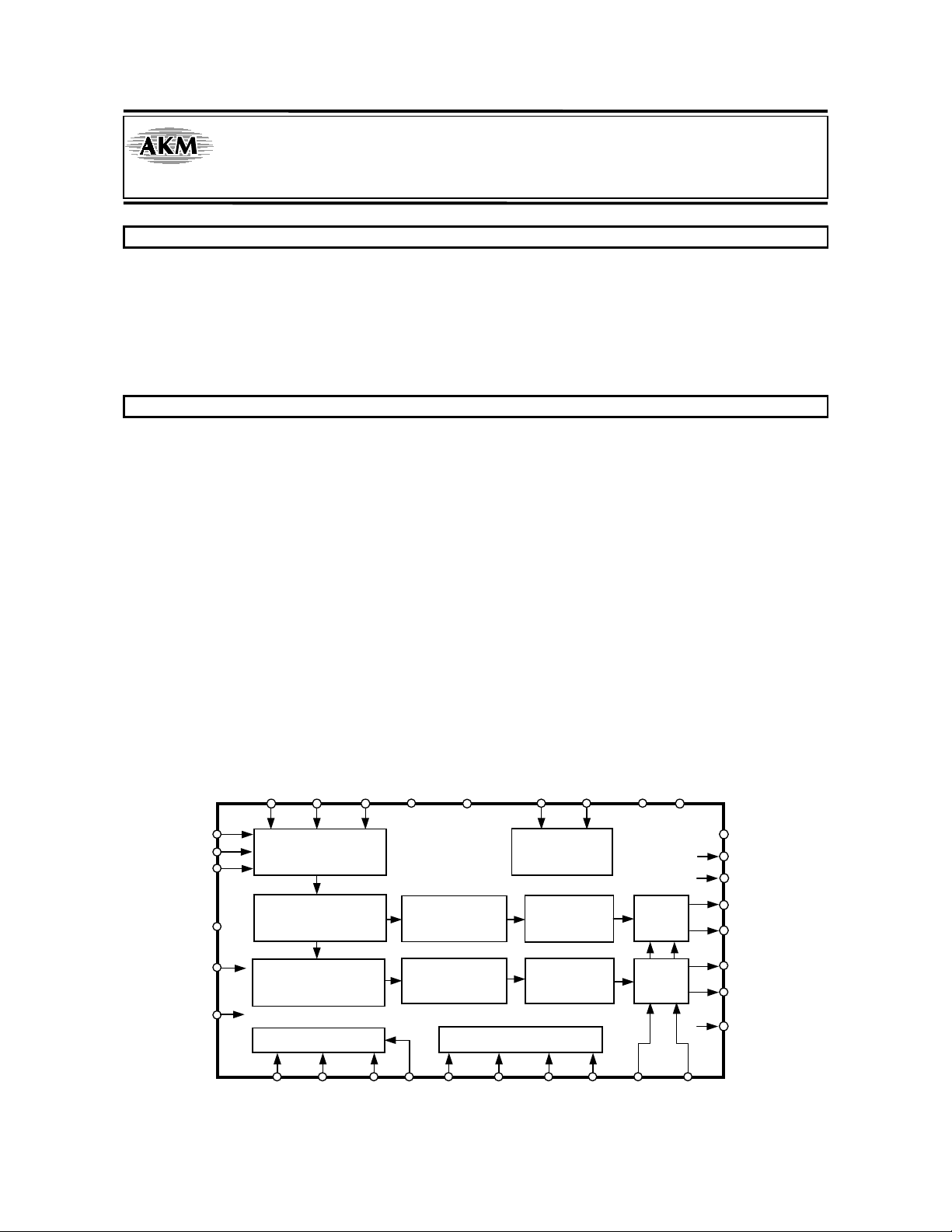
LRCK
BICK
SDAT
PDN
SMUTE
DFS0
Audio Data
Interface
De-emphasis
Soft Mute
De-emphasis
Soft Mute
DIF2DIF1DIF0
DEM0DVDD
DEM1
De-emphasis
Control
8x
Interpolator
8x
Interpolator
DS
Modulator
DS
Modulator
AVDD
SCF
AVSSDVSS
BVSS
VCOM
DZFL
AOUTL+
SCF
AOUTL-
AOUTR+
AOU TR-
DZFR
Control Register Clock Divider
CSN
CCLK
CDTI
P/S
MCLK CKS0
CKS1 CKS2 VREFH VREFL
M0081-E-00 1999/11
- 1 -
ASAHI KASEI
n Ordering Guide
AK4394VF -40 ~ +85 °C 28pin VSOP (0.65mm pitch)
AKD4394 Evaluation Board
n
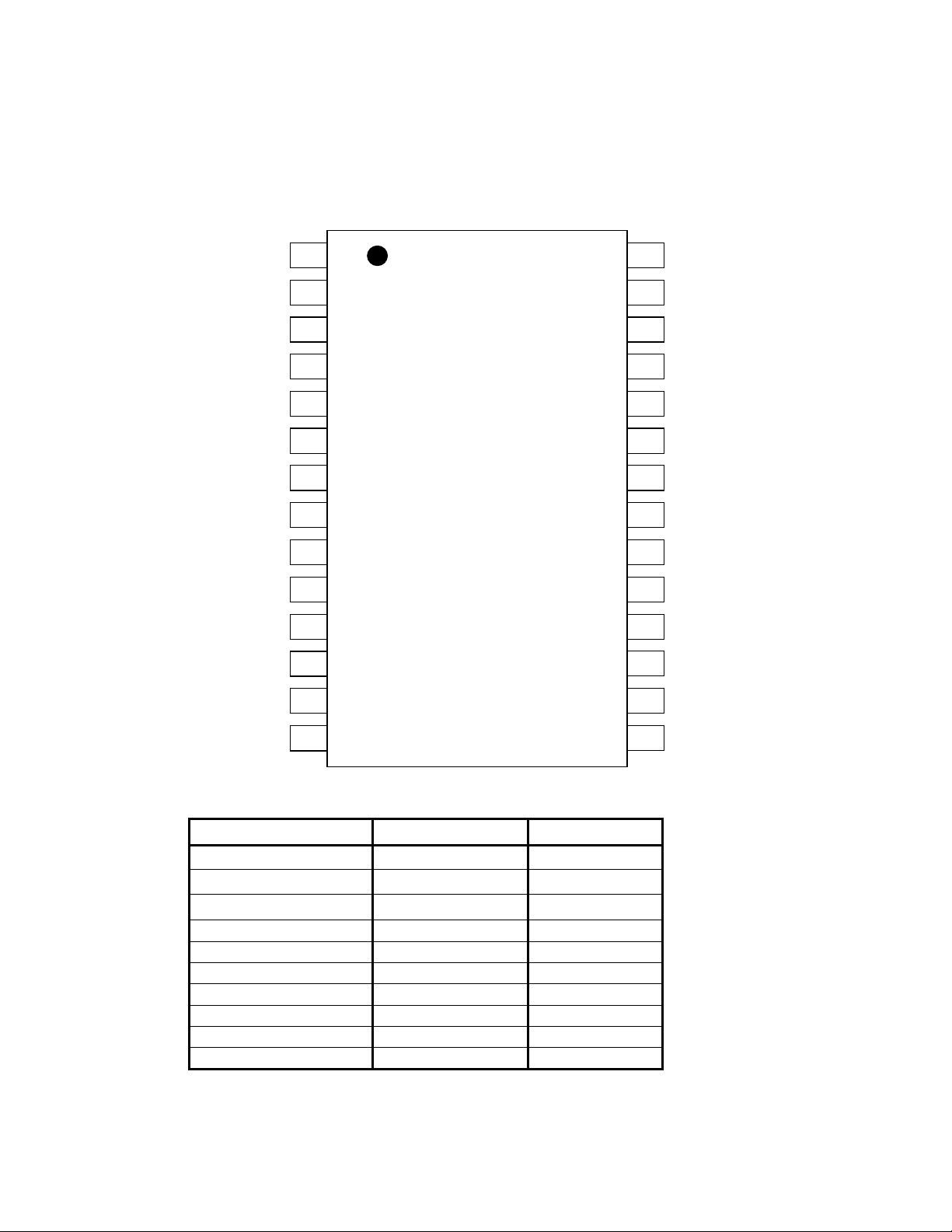
n Pin Layout
nn
[AK4394]
DVSS
DVDD
MCLK
PDN
BICK
SDATA
LRCK 7
SMUTE/CSN 8
DFS0
DEM0/CCLK
DEM1/CDTI 11
DIF0 12
DIF1
10
13
1
2
3
4
5
6
Top
View
9
28
27
26
25
24
23
22
21
20
19
18
17
16
CKS2/DZFR
CKS1
CKS0/DZFL
P/S
VCOM
AOUTL
+
AOUTL-
AOUTR+
AOUTR-
AVSS
AVDD
VREFH
VREFL
DIF2
n
n Pin Compatibility with AK4393
nn
14
15
BVSS
AK4393 AK4394
fs (max) 108kHz 216kHz
slow roll-off filter not available available
zero detection not available available
DVDD 3~5.25V 4.75~5.25V
pin #26 (serial mode) CKS0 DZFL
pin #28 (serial mode) CKS2 DZFR
Control register : 01H D4 0 DFS1
Control register : 01H D5 0 SLOW
Control register : 01H D6 0 DZFM
Control register : 01H D7 0 DZFE
M0081-E-00 1999/11
- 2 -
ASAHI KASEI
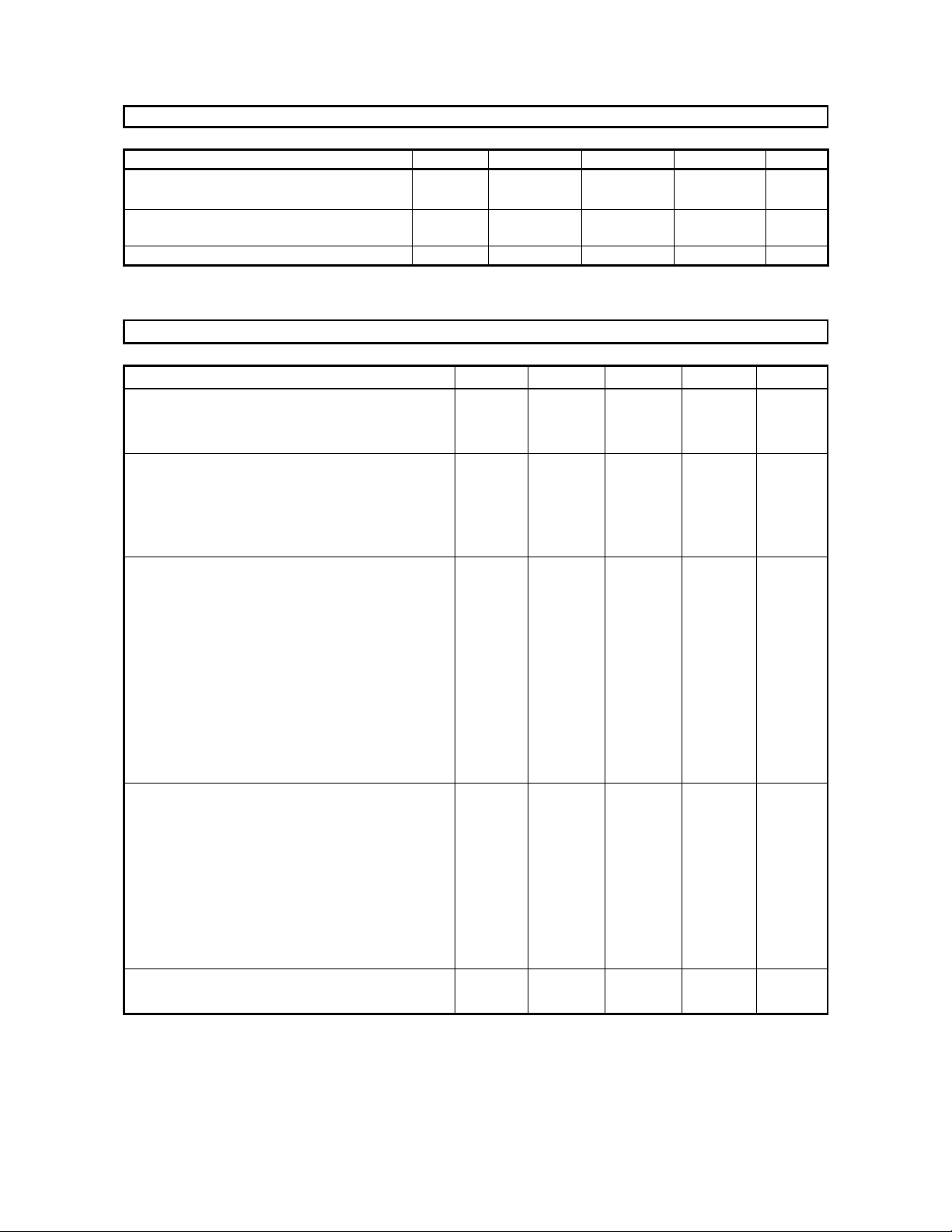
PIN/FUNCTION
No. Pin Name I/O Function
1 DVSS - Digital Ground Pin
2 DVDD - Digital Power Supply Pin, 5.0V
3 MCLK I Master Clock Input Pin
PDN I Power-Down Mode Pin
4
When at “L”, the AK4394 is in power-down mode and is held in reset.
The AK4394 should always be reset upon power-up.
BICK I Audio Serial Data Clock Pin
5
SDATA I Audio Serial Data Input Pin
6
The clock of 64fs or more than is recommended to be input on this pin.
2’s complement MSB-first data is input on this pin.
7 LRCK I L/R Clock Pin
SMUTE I Soft Mute Pin in parallel mode
8
When this pin goes "H", soft mute cycle is initiated.
When returning “L”, the output mute releases.
CSN I Chip Select Pin in serial mode
DFS0 I Double Speed Sampling Mode Pin (Internal pull-down pin)
9
DEM0 I De-emphasis Enable Pin in parallel mode
10
CCLK I Control Data Clock Pin in serial mode
DEM1 I De-emphasis Enable Pin in parallel mode
11
CDTI I Control Data Input Pin in serial mode
“L”: Normal Speed , “H”: Double Speed
12 DIF0 I Digital Input Format Pin
13 DIF1 I Digital Input Format Pin
14 DIF2 I Digital Input Format Pin
15 BVSS - Sub strate Ground Pin, 0V
16 VREFL I Low Level Voltage Reference Input Pin
17 VREFH I High Level Voltage Reference Input Pin
18 AVDD - Analog Power Supply Pin, 5.0V
19 AVSS - Analog Ground Pin, 0V
20 AOUTR- O Rch Negative analog output Pin
21 AOUTR+ O Rch Positive analog output Pin
22 AOUTL- O Lch Negative analog output Pin
23 AOUTL+ O Lch Positive analog output Pin
24 VCOM O Common Voltage Output Pin, 2.6V
25 P/S I Parallel/Serial Select Pin (Internal pull-up pin)
“L”: Serial control mode, “H”: Parallel control mode
CKS0 I Master Clock Select Pin in parallel mode
26
DZFL O Lch Zero Input Detect Pin in serial mode
27 CKS1 I Master Clock Select Pin
CKS2 I Master Clock Select Pin in pa rallel mode
28
DZFR O Rch Zero Input Detect Pin in serial mode
[AK4394]
Note: All input pins except internal pull-up/down pins should not be left floating.
M0081-E-00 1999/11
- 3 -
ASAHI KASEI
[AK4394]
ABSOLUTE MAXI MUM RATINGS
(AVSS, BVSS, DVSS = 0V; Note 1)
Parameter Symbol min max Units
Power Supplies: Analog
Digital
| BVSS-DVSS | (Note 2)
Input Current , Any pin Except Supplies IIN Input Voltage VIND -0.3 DVDD+0.3 V
Ambient Operating Temperature Ta -40 85
Storage Temperature Tstg -65 150
Notes: 1. All voltages with respect to ground.
2. AVSS, BVSS and DVSS must be connected to the same analog ground plane.
WARNING: Operation at or beyond these limits may result in permanent damage to the device.
Normal operation is not guaranteed at these extremes.
AVDD
DVDD
GND
D
-0.3
-0.3
-
6.0
6.0
0.3
±
10
mA
RECOMMENDED OPERATING CONDITIONS
(AVSS, BVSS, DVSS=0V; Note 1)
Parameter Symbol min typ max Units
Power Supplies:
(Note 3)
Voltage Reference
(Note 4)
Notes: 3. The power up sequence between AVDD and DVDD is not critical.
4. Analog output voltage scales with the voltage of (VREFH-VREFL).
AOUT (typ.@0dB) = (AOUT+) - (AOUT-) = ±2.4Vpp×(VREFH-VREFL)/5.
Analog
Digital
“H” voltage reference
“L” voltage refer ence
VREFH-VREFL
AVDD
DVDD
VREFH
VREFL
VREF
D
4.75
4.75
AVDD-0.5
AVSS
3.0
5.0
5.0
5.25
5.25
-
-
-
AVDD
-
AVDD
V
V
V
C
°
C
°
V
V
V
V
V
* AKM assumes no responsibility for the usage beyond the conditions in this data sheet.
M0081-E-00 1999/11
- 4 -
ASAHI KASEI
[AK4394]
ANALOG CHARACTERISTICS
(Ta = 25°C; AVDD, DVDD = 5V; AVSS, BVSS, DVSS = 0V, VREFH = AVDD, VREFL = AVSS;
fs = 44.1kHz; BICK = 64fs; Signal Frequency = 1kHz; 24bit Input Data; Measurement Bandwidth = 20Hz~20kHz;
600W; External circuit: Figure 12; unless otherwise specified)
R
³
L
Parameter min typ max Units
Resolution 24 Bits
Dynamic Characteristics
THD+N
Dynamic Range (-60dBFS with A-weighted) (Note 6)
(Note 7)
S/N (A-weighted (Note 8)
(Note 7)
(Note 5)
fs=44.1kHz
BW=20kHz
fs=96kHz
BW=40kHz
fs=192kHz
BW=40kHz
0dBFS
-60dBFS
0dBFS
-60dBFS
0dBFS
-60dBFS
112
-
112
-
-100
-53
-97
-51
-97
-51
117
120
117
120
-90
-87
dB
-
dB
dB
-
-
-
dB
dB
dB
dB
dB
dB
dB
Interchannel Isolation (1kHz) 100 120 dB
DC Accuracy
Interchannel Gain Mismatch 0.15 0.3 dB
Gain Drift (Note 9) 20 - ppm/°C
Output Voltage (Note 10)
Load Resistance (Note 11) 600
±
2.25
2.4
±
2.55 Vpp
±
W
Output Current 3.5 mA
Power Supplies
Power Supply Current
Normal Operation (PDN = “H”)
AVDD
DVDD(fs=44.1kHz)
DVDD(fs=96kHz)
DVDD(fs=192kHz)
AVDD + DVDD
60
12
-
5
8
-
-
-
90
mA
mA
mA
mA
mA
Power-Down Mode (PDN = “L”)
AVDD + DVDD (Note 12) 10 100 µA
Power Supply Rejection (Note 13) 50 dB
Notes: 5. At 44.1kHz, measured by Audio Precision, System Two. Averaging mode.
At 96kHz and 192kHz, measured by ROHDE & SCHWARZ, UPD. Averaging mode.
Refer to the eva board manual.
6. 101dB at 16bit data and 116dB at 20bit data.
7. By Figure13. External LPF Circuit Example 2.
8. S/N does not depend on input bit length.
9. The voltage on (VREFH-VREFL) is held +5V externally.
10. Full-scale voltage(0dB). Output voltage scales with the voltage of (VREFH-VREFL).
AOUT (typ.@0dB) = (AOUT+) - (AOUT-) = ±2.4Vpp×(VREFH-VREFL)/5.
11. For AC-load. 1kW for DC-load.
12. In the power-down mode. P/S = DVDD, and all other digital input pins including clock pins (MCLK, BICK and
LRCK) are held DVSS.
13. PSR is applied to AVDD, DVDD with 1kHz, 100mVpp. VREFH pin is held +5V.
M0081-E-00 1999/11
- 5 -

ASAHI KASEI
[AK4394]
SHARP ROLL-OFF FILTER CHARACTERISTICS ( f s = 44.1kHz)
(Ta = 25°C; AVDD, DVDD = 4.75~5.25V; fs = 44.1kHz; Normal Speed Mode; DEM = OFF; SLOW = “0”)
Parameter Symbol min typ max Units
Digital Filter
Passband ±0.01dB (Note 14)
-6.0dB
Stopband (Note 14) SB 24.1 kHz
Passband Ripple PR
Stopband Attenuation SA 75 dB
Group Delay (Note 15) GD - 28 - 1/fs
Digital Filter + SCF
Frequency Response 0 ~ 20.0kHz -
Note: 14. The passband and stopband frequencies scale with fs.
For example, PB = 0.4535×fs (@±0.01dB), SB = 0.546×fs.
15. The calculating delay time which occurred by digital filtering. This time is from setting the 16/20/24bit data of
both channels to input register to the output of analog signal.
PB 0
- 22.05
0.2 - dB
±
20.0
-
0.005 dB
±
kHz
kHz
SHARP ROLL-OFF FILTER CHARACTERISTICS (fs = 96kHz)
(Ta = 25°C; AVDD, DVDD = 4.75~5.25V; fs = 96kHz; Double Speed Mode; DEM = OFF; SLOW = “0”)
Parameter Symbol min typ max Units
Digital Filter
Passband ±0.01dB (Note 14)
-6.0dB
Stopband (Note 14) SB 52.5 kHz
Passband Ripple PR
Stopband Attenuation SA 75 dB
Group Delay (Note 15) GD - 28 - 1/fs
Digital Filter + SCF
Frequency Response 0 ~ 40.0kHz -
PB 0
- 48.0
0.3 - dB
±
43.5
-
0.005 dB
±
kHz
kHz
SHARP ROLL-OFF FILTER CHARACTERISTICS (fs = 192kHz)
(Ta = 25°C; AVDD, DVDD = 4.75~5.25V; fs = 192kHz; Quad Speed Mode; DEM = OFF; SLOW = “0”)
Parameter symbol min typ max Units
Digital Filter
Passband ±0.01dB (Note 14)
-6.0dB
Stopband (Note 14) SB 105 kHz
Passband Ripple PR
Stopband Attenuation SA 75 dB
Group Delay (Note 15) GD - 28 - 1/fs
Digital Filter + SCF
Frequency Response 0 ~ 80.0kHz - +0/-1 - dB
M0081-E-00 1999/11
PB 0
- 6 -
- 96.0
87.0
-
0.005 dB
±
kHz
kHz
ASAHI KASEI
[AK4394]
SLOW ROLL-OFF FILTER CHA RACTERISTICS (fs = 44.1kHz)
(Ta = 25°C; AVDD, DVDD = 4.75~5.25V; fs = 44.1kHz; Normal Speed Mode; DEM = OFF; SLOW = “1”)
Parameter Symbol min typ max Units
Digital Filter
Passband ±0.04dB (Note 16)
-3.0dB
Stopband (Note 16) SB 39.2 kHz
Passband Ripple PR
Stopband Attenuation SA 72 dB
Group Delay (Note 15) GD - 28 - 1/fs
Digital Filter + SCF
Frequency Response 0 ~ 20.0kHz - +0/-5 - dB
Note: 16. The passband and stopband frequencies scale with fs.
For example, PB = 0.185×fs (@±0.04dB), SB = 0.888×fs.
PB 0
- 18.2
8.1
-
0.005 dB
±
kHz
kHz
SLOW ROLL-OFF FILTER CHARACTERISTICS (fs = 96kHz)
(Ta = 25°C; AVDD, DVDD = 4.75~5.25V; fs = 96kHz; Double Speed Mode; DEM = OFF; SLOW = “1”)
Parameter Symbol min typ max Units
Digital Filter
Passband ±0.04dB (Note 16)
-3.0dB
Stopband (Note 16) SB 85.3 kHz
Passband Ripple PR
Stopband Attenuation SA 72 dB
Group Delay (Note 15) GD - 28 - 1/fs
Digital Filter + SCF
Frequency Response 0 ~ 40.0kHz - +0/-4 - dB
PB 0
- 39.6
17.7
-
0.005 dB
±
kHz
kHz
SLOW ROLL-OFF FILTER CHARACTERISTICS (fs = 192kHz)
(Ta = 25°C; AVDD, DVDD = 4.75~5.25V; fs = 192kHz; Quad Speed Mode; DEM = OFF; SLOW = “1”)
Parameter Symbol min typ max Units
Digital Filter
Passband ±0.04dB (Note 16)
-3.0dB
Stopband (Note 16) SB 171 kHz
Passband Ripple PR
Stopband Attenuation SA 72 dB
Group Delay (Note 15) GD - 28 - 1/fs
Digital Filter + SCF
Frequency Response 0 ~ 80.0kHz - +0/-5 - dB
M0081-E-00 1999/11
PB 0
- 7 -
- 79.1
35.5
-
0.005 dB
±
kHz
kHz
ASAHI KASEI
[AK4394]
DC CHARACTERISTICS
(Ta = 25°C; AVDD, DVDD = 4.75~5.25V)
Parameter Symbol min typ max Units
High-Level Input Voltage
Low-Level Input Voltage
High-Level Output Voltage (Iout = -1 00mA)
Low-Level Output Voltage (Iout = 100mA)
Input Leakage Current (Note 17) Iin - -
Note: 17. DFS0, P/S pins have internal pull-down or pull-up devices, nominally 100kW.
VIH
VIL
VOH
VOL
2.2
-
DVDD-0.5
-
-
-
-
-
±
0.8
0.5
10
-
-
V
V
V
V
µA
SWITCHING CHARACTERISTICS
(Ta = 25°C; AVDD, DVDD = 4.75~5.25V; CL = 20pF)
Parameter Symbol min typ max Units
Master Clock Timing
Frequency
Duty Cycle
LRCK Frequency
Normal Speed Mode
Double Speed Mode
Quad Speed Mode
Duty Cycle
Serial Interface Timing
BICK Period
BICK Pulse Width Low
Pulse Width High
BICK “” to LRCK Edge (Note 19)
LRCK Edge to BICK “” (Note 19)
SDATA Hold Time
SDATA Setup Time
Control Interface Timing
CCLK Period
CCLK Pulse Width Low
Pulse Width High
CDTI Setup Time
CDTI Hold Time
CSN High Time
CSN “¯” to CCLK “”
CCLK “” to CSN “”
Reset Timing
PDN Pulse Width (Note 20) tPD 150 ns
Notes: 18. When the normal/double/quad speed m odes are switched, AK4394 should be reset by PDN pin or RS TN bit.
19. BICK rising edge must not occur at the same time as LRCK edge.
20. The AK4394 can be reset by bringing PDN “L” to “H”.
When the states of CKS2-0 or DFS1-0 change, the AK4394 should be reset by PDN pin or RSTN bit.
(Note 18)
Normal Speed Mode
Double Speed Mode
Quad Speed Mode
fCLK
dCLK
fsn
fsd
fsq
Duty
tBCK
tBCK
tBCK
tBCKL
tBCKH
tBLR
tLRB
tSDH
tSDS
tCCK
tCCKL
tCCKH
tCDS
tCDH
tCSW
tCSS
tCSH
7.7
40
30
60
120
45
1/128fs
1/64fs
1/64fs
30
30
20
20
20
20
200
80
80
50
50
150
50
50
41.472
60
54
108
216
55
MHz
%
kHz
kHz
kHz
%
ns
ns
ns
ns
ns
ns
ns
ns
ns
ns
ns
ns
ns
ns
ns
ns
ns
M0081-E-00 1999/11
- 8 -
 Loading...