

ASAHI KASEI [AK4382]
AK4382
DS
112dB 192kHz 24-Bit 2ch
GENERAL DESCRIPTIO N
The AK4382 offers the perfect mix for cost and performance based audio systems. Using AKM's multi bit
architecture for its modulator the AK4382 delivers a wide dynamic range while preserving linearit y for
improved THD+N performance. The AK4382 has full differential SCF outputs, removing the need for AC
coupling capacitors and increasing performance for systems with excessive clock jitter. The 24 Bit word
length and 192kHz sampling rate make this part ideal for a wide range of applications including DVDAudio. The AK4382 is offered in a space saving 16pin TSSOP package.
FEATURES
o Sampling Rate Ranging from 8kHz to 192kHz
o 128 times Oversampling (Normal Speed Mode)
o 64 times Oversampling (Double Speed Mode)
o 32 times Oversampling (Quad Speed Mode)
o 24-Bit 8 times FIR Digital Filter
o On chip SCF
o Digital de-emphasis for 32k, 44.1k and 48kHz sampling
o Soft mute
o Digital Attenuator (256 steps)
o I/F format: 24-Bit MSB justified, 24/20/16-Bit LSB justified or I
o Master clock: 256fs, 384fs, 512fs or 768fs (Normal Speed Mode)
128fs, 192fs, 256fs or 384fs (Double Speed Mode)
128fs, 192fs (Quad Speed Mode)
o THD+N: -94dB
o Dynamic Range: 112dB
o High Tolerance to Clock Jitter
o Power supply: 4.75 to 5.25V
o Very Small Package: 16pin TSSOP (6.4mm x 5.0mm)
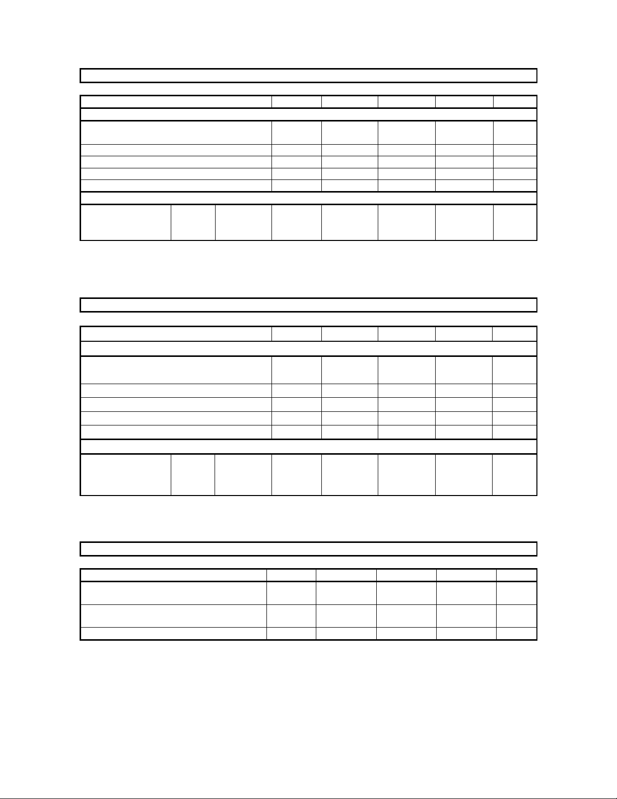
2
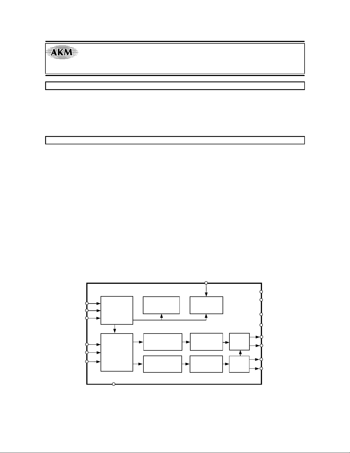
S
DAC
MCLK
VDD
CSN
CCLK
CDTI
LRCK
BICK
SDTI
MS0034-E-00 2000/7
µP
Interface
Audio
Data
Interface
PDN
De-emphasis
Control
8X
Interpolator
8X
Interpolator
- 1 -
Clock
Divider
DS
Modulator
DS
Modulator
SCF
SCF
VSS
DZFL
DZFR
AOUTL+
AOUTL-
AOUTR+
AOUTR-
ASAHI KASEI [AK4382]
n Ordering Guide
AK4382VT -40 ~ +85°C 16pin TSSOP (0.65mm pitch)
AKD4382 Evaluation Board for AK4382
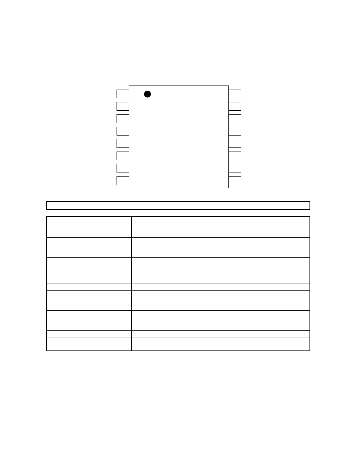
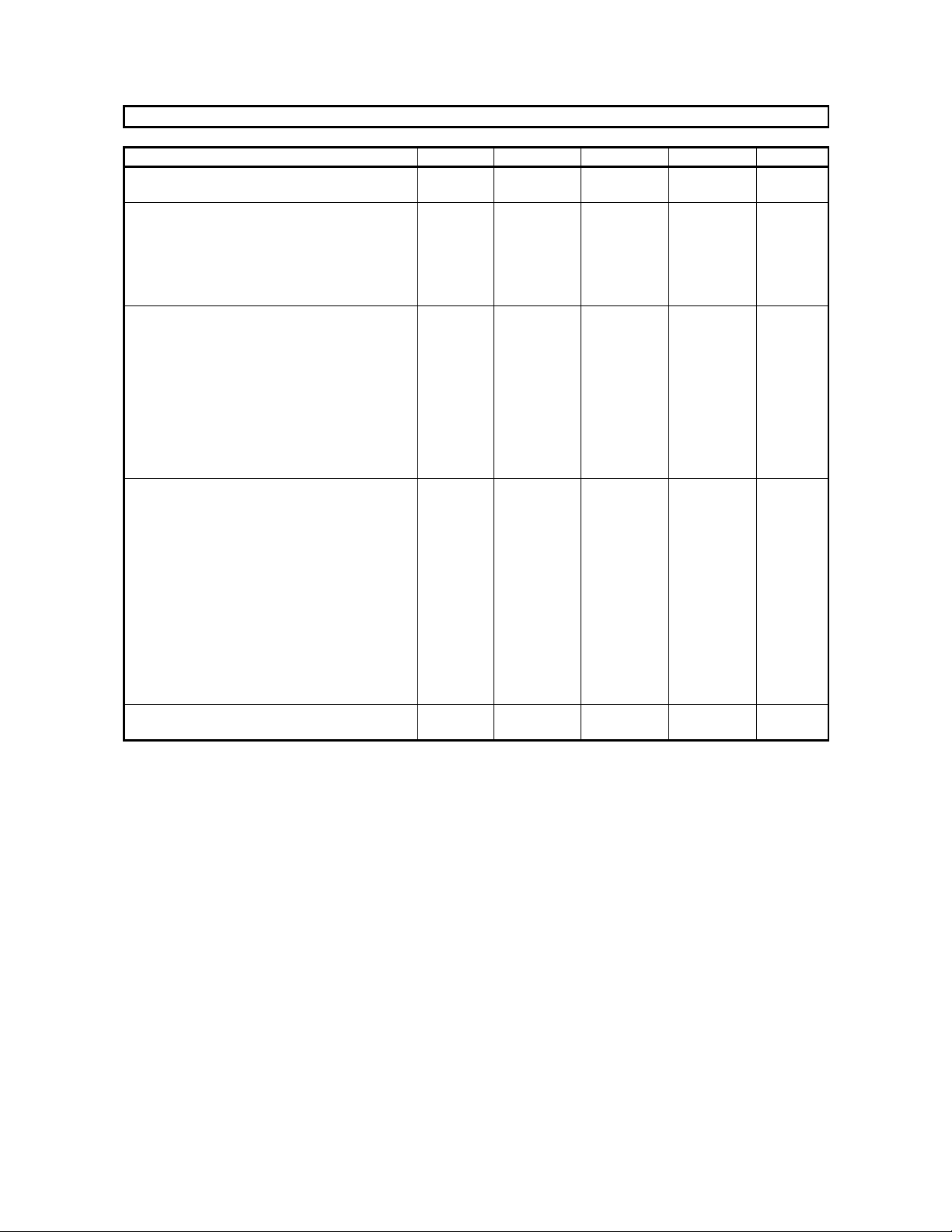
n Pin Layout
MCLK
BICK
SDTI
LRCK
PDN
CSN
CCLK
CDTI
1
2
3
4
5
6
7
8
Top
View
PIN/FUNCTION
No. Pin Name I/O Function
1 MCLK I Master Clock Input Pin
An external TTL clock should be input on this pin.
2 BICK I Audio Serial Data Clock Pin
3 SDTI I Audio Serial Data Input Pin
4 LRCK I L/R Clock Pin
5 PDN I Power-Down Mode Pin
When at “L”, the AK4382 is in the power-down mode and is held in reset.
The AK4382 should always be reset upon power-up.
6 CSN I Chip Select Pin
7 CCLK I Control Data Input Pin
8 CDTI I Control Data Input Pin in serial mode
9 AOUTR- O Rch Negative Analog Output Pin
10 AOUTR+ O Rch Positive Analog Output Pin
11 AOUTL- O Lch Negative Analog Output Pin
12 AOUTL+ O Lch Positive Analog Output P in
13 VSS - Ground Pin
14 VDD - Power Supply Pin
15 DZFR O Rch Data Zero Input Detect Pin
16 DZFL O Lch Data Zero Input Detect Pin
Note: All input pins should not be left floating.
16
15
14
13
12
11
10
DZFL
DZFR
VDD
VSS
AOUTL+
AOUTL-
AOUTR+
9
AOUTR-
MS0034-E-00 2000/7
- 2 -
ASAHI KASEI [AK4382]
ABSOLUTE MAXI MUM RATINGS
(VSS=0V; Note 1)
Parameter Symbol min max Units
Power Supply VDD -0.3 6.0 V
Input Current (any pins except for supplies) IIN Input Voltage VIND -0.3 VDD+0.3 V
Ambient Operating Temperature Ta -40 85
Storage Temperature Tstg -65 150
Note: 1. All voltages with respect to ground.
WARNING: Operation at or beyond these limits may results in permanent damage to the device.
Normal operation is not guaranteed at these extremes.
±10
mA
°C
°C
RECOMMENDED OPERATING CONDITIONS
(VSS=0V; Note 1)
Parameter Symbol min typ max Units
Power Supply VDD 4.75 5.0 5.25 V
*AKM assumes no responsibility for the usage beyond the conditions in this datasheet.
MS0034-E-00 2000/7
- 3 -
ASAHI KASEI [AK4382]
ANALOG CHARACTERISTICS
(Ta=25°C; VDD=5.0V; fs=44.1kHz; BICK=64fs; Signal Frequency=1kHz; 24bit Input Data;
Measurement frequency=20Hz ~ 20kHz; R
³2kW; unless otherwise specified)
L
Parameter min typ max Units
Resolution 24 Bits
Dynamic Characteristics (Note 3)
THD+N
fs=44.1kHz
BW=20kHz
fs=96kHz
BW=40kHz
fs=192kHz
BW=40kHz
0dBFS
-60dBFS
0dBFS
-60dBFS
0dBFS
-60dBFS
-94
-48
-92
-45
-92
-45
-86
-84
dB
-
dB
dB
-
-
-
dB
dB
dB
Dynamic Range (-60dBFS with A-weighted) (Note 4) 102 112 dB
S/N (A-weighted) (Note 5) 102 112 dB
Interchannel Isolation (1kHz) 90 110 dB
Interchannel Gain Mismatch 0.2 0.5 dB
DC Accuracy
Gain Drift 100 Output Voltage (Note 6)
±2.55 ±2.75 ±2.95
Load Resistance (Note 7) 2
ppm/°C
Vpp
kW
Power Supplies
Power Supply Current (VDD)
Normal Operation (PDN = “H”, fs£96kHz)
Normal Operation (PDN = “H”, fs=192kHz)
Power-Down Mode (PDN = “L”) (Note 8)
20
25
10
34
42
100
mA
mA
µA
Notes: 3. Measured by Audio Precision (System Two). Refer to the evaluation board manual.
4. 100dB at 16bit data.
5. S/N does not depend on input bit length.
6. Full-scale voltage (0dB). Output voltage scales with the voltage of VREF,
AOUT (typ.@0dB)=(AOUT+)-(AOUT-)=±2.75Vpp × VREF/5.
7. For AC-load. 4kW for DC-load.
8. All digital inputs including clock pins (MCLK, BICK and LRCK) are held VDD or VSS.
MS0034-E-00 2000/7
- 4 -
ASAHI KASEI [AK4382]
SHARP ROLL-OFF FILTER CHARACTERISTICS
(Ta = 25°C; VDD = 4.75 ~ 5.25V; fs = 44.1kHz; DEM = OFF; SLOW = “0”)
Parameter Symbol min typ max Units
Digital filter
Passband ±0.05dB (Note 9)
-6.0dB
Stopband (Note 9) SB 24.25 KHz
Passband Ripple PR
Stopband Attenuation SA 54 DB
Group Delay (Note 10) GD - 19.3 - 1/fs
Digital Filter + LPF
Frequency Response 20.0kHz
40.0kHz
80.0kHz
Notes: 9. The passband and stopband frequencies scale with fs(system sampling rate).
For example, PB=0.4535×fs (@±0.05dB), SB=0.546×fs.
10. The calculating delay time which occurred by digital filtering. This time is from setting the 16/24bit data
of both channels to input register to the output of analog signal.
fs=44.1kHz
fs=96kHz
fs=192kHz
PB 0
FR
FR
FR
- 22.05
-
-
-
± 0.2
± 0.3
+0/-0.6
20.0
-
± 0.02
-
-
-
KHz
KHz
DB
Db
dB
dB
SLOW ROLL-OFF FILTER CHA RACTERISTICS
(Ta = 25°C; AVDD, DVDD = 4.75~5.25V; fs = 44.1kHz; DEM = OFF; SLOW = “1”)
Parameter Symbol min typ max Units
Digital Filter
Passband ±0.04dB (Note 11)
-3.0dB
Stopband (Note 11) SB 39.2 kHz
Passband Ripple PR ± 0.005 dB
Stopband Attenuation SA 72 dB
Group Delay (Note 10) GD - 19.3 - 1/fs
Digital Filter + SCF
Frequency Response
Note: 11. The passband and stopband frequencies scale with fs.
For example, PB = 0.185×fs (@±0.04dB), SB = 0.888×fs.
20.0kHz
40.0kHz
80.0kHz
fs=44.kHz
fs=96kHz
fs=192kHz
PB 0
FR
FR
FR
- 18.2
-
-
-
+0/-5
+0/-4
+0/-5
8.1
kHz
-
-
-
-
kHz
dB
dB
dB
DC CHARACTERISTICS
(Ta=25°C; VDD=4.5 ~ 5.5V)
Parameter Symbol min typ max Units
High-Level Input Voltage
Low-Level Input Voltage
High-Level Output Voltage (Iout=-80µA)
Low-Level Output Voltage (Iout=80µA)
Input Leakage Current Iin - -
MS0034-E-00 2000/7
VIH
VIL
VOH
VOL
- 5 -
2.2
-
VDD-0.4
-
-
-
--
-
0.8
0.4
± 10
V
V
V
V
µA
ASAHI KASEI [AK4382]
SWITCHING CHARACTERISTICS
(Ta=25°C; VDD=4.5 ~ 5.5V; CL=20pF)
Parameter Symbol min typ max Units
Master Clock Frequency
Duty Cycle
LRCK Frequency
Normal Speed Mode
Double Speed Mode
Quad Speed Mode
Duty Cycle
Audio Interface Timing
BICK Period
Normal Speed Mode
Double/Quad Speed Mode
BICK Pulse Width Low
Pulse Width High
BICK rising to LRCK Edge (Note 12)
LRCK Edge to BICK rising (Note 12)
SDTI Hold Time
SDTI Setup Time
Control Interface Timing
CCLK Period
CCLK Pulse Width Low
Pulse Width High
CDTI Setup Time
CDTI Hold Time
CSN “H” Time
CSN “¯” to CCLK “”
CCLK “” to CSN “”
Rise Time of CSN
Fall Time of CSN
Rise Time of CCLK
Fall Time of CCLK
Reset Timing
PDN Pulse Width (Note 13)
Notes: 12. BICK rising edge must not occur at the same time as LRCK edge.
13. The AK4382 can be reset by bringing PDN= “L”.
fCLK
dCLK
fsn
fsd
fsq
Duty
tBCK
tBCK
tBCKL
tBCKH
tBLR
tLRB
tSDH
tSDS
tCCK
tCCKL
tCCKH
tCDS
tCDH
tCSW
tCSS
tCSH
tR1
tF1
tR2
tF2
tPD 100 ns
2.048
40
8
60
120
45
1/128fs
1/64fs
30
30
20
20
20
20
200
80
80
40
40
150
50
50
11.2896 36.864
60
48
96
192
55
20
20
20
20
MHz
%
kHz
kHz
kHz
%
ns
ns
ns
ns
ns
ns
ns
ns
ns
ns
ns
ns
ns
ns
ns
ns
ns
ns
ns
ns
MS0034-E-00 2000/7
- 6 -
ASAHI KASEI [AK4382]
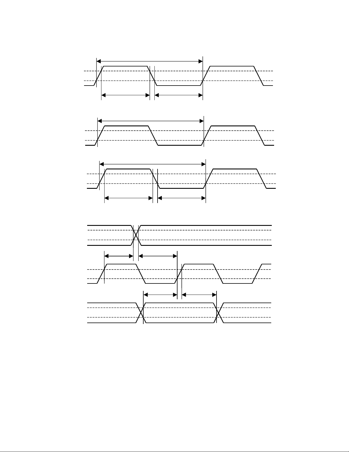
n Timing Diagram
1/fCLK
MCLK
LRCK
BICK
LRCK
tCLKH
tBCKH
1/fs
tBCK
Clock Timing
tCLKL
tBCKL
VIH
VIL
dCLK=tCLKH x fCLK, tCLKL x fCLK
VIH
VIL
VIH
VIL
VIH
VIL
BICK
SDTI
tBLR
tLRB
tSDS
tSDH
Serial Interface Timing
VIH
VIL
VIH
VIL
MS0034-E-00 2000/7
- 7 -
 Loading...