

AKM AK4317-VF Datasheet

ASAHI KASEI [AK4317]
AK4317
18Bit SCF DAC with ATT & MIXER
General Description
The AK4317 is a 1bit stereo DAC with channel separated volume and channel mixer. This DAC also
includes 18bit dig it al f ilter and analog LPF. A 1bit DAC can achieve monoto n i c it y and low distortion with
no adjustment and is superior to traditional R-2R ladd er based DACs. In the AK4317, the loss of
accuracy from clock jitter is also improved by using SCF techniques for on-chip post filter. Therefore, the
AK4317 is suitab le for the system like STB including PLL circuit.
Features
Sampling Rate Ranging from 8kHz to 50kHz
On chip Perfect filtering
•
8 times FIR Interpolator
•
2nd order SCF
•
2nd order CTF
Digital de-emphasis for 32, 44.1, 48kHz sampling
L/R Separated Volume
L/R Mixing
Soft Mute
Audio I/F format : MSB justified, LSB justified, I2S
Master Clock: 256fs or 384fs
High Tolerance to Clock Jitter
THD+N: -86dB
DR: 92dB
Power Supply:4.5 to 5.5V
Small Package: 24pin VSOP
AK4311 Compatible
0172-E-01 1997/5
- 1 -
ASAHI KASEI [AK4317]
Ordering Guide
AK4317-VF -40∼+85°C 24pin VSOP(0.65mm pitch)
AKD4317 Evaluation B oard
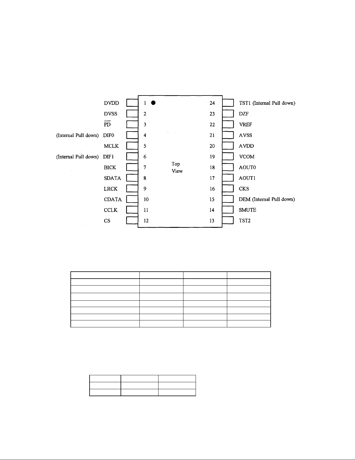
Pin Layout
Compatibility with AK4311/A
1. Changed Specs
Parameter AK4311 AK4311A AK4317
Resolution 16bit 16bit 16/18bit
Operating Temperature
Power Supply
Digital I/F level CMOS CMOS TTL
X'tal Oscillator Yes Yes No
DR 92dB 91dB 92dB
Package SSOP SSOP VSOP
-40∼85°C-10
3∼5.5V 3∼5.5V 4.5∼5.5V
C-40
∼70°
∼85°
C
2. Pin Compatibi lity
The following pin functions are changed fr om AK4311/A. But when X'tal oscillating circuit is not used, it
is possible to chan ge A K4311/A to AK4317 without changing the board layout.
Pin No. AK4311/A AK4317
4XTODIF0
6CLKODIF1
0172-E-01 1997/5
- 2 -
ASAHI KASEI [AK4317]
PIN/FUNCTION
No. Pin Name I/O Function
1 DVDD - Digital Power Supply
2 DVSS - Digital Ground Pin
3 PD I Power-Do wn Mode Pin
When at "L", the AK4317 is in p ower-down mode and is held in reset.
The AK4317 should always be reset upon po wer-up.
4 DIF0 I Digital Input Format Pin (Internal Pull-down pin)
5 MCLK I Master Clock Input Pin
6 DIF1 I Digital Input Format Pin (Internal Pull-down pin)
7 BICK I Audio S erial Data Clock Pin
8 SDATA I Audio Serial Data Input Pin
2's complement MSB-first data is input on t his pin.
9 LRCK I L/R Clock Pin
10 CDATA I Control Data Input Pi n
Must be tied to "H" or "L" if this pin is not used.
11 CCLK I Control Clock Pin
Must be tied to "H" or "L" if this pin is not used.
12 CS I Chip Select Pin
Must be tied to "H" if this pin is not used.
13 TST2 O Test Pin
Must be left floating.
14 SMUTE I Soft Mute Pin
When this pin goes "H", soft mute cycle is initiated.
When returning "L", the output mute releases.
15 DEM I De-emphasis Enable Pin (Internal Pull-dow n pin)
16 CKS I Master Clock Select Pin
MCLK=256fs,"H": MCLK=384fs
17 AOUT1 O Channel 1 analog output pin
18 AOUT0 O Channel 0 analog output pin
19 VCOM I Common Voltage Pin, AVDD/2
Normally connected to AVSS with a 0.1uF ceram ic capacitor in paralle l
with a 10uF electrolytic cap.
20 AVDD - Analog Power Supply Pin
21 AVSS - Analog Ground pin
22 VREF I Voltage Reference Input Pin
The differential Voltage between this pin and AVSS set the analog output
range. Normally connected t o AVSS with a 0.1uF cerami c capacitor .
23 DZF O Zero Input D etect Pin
24 TST1 I T est Pin
Must be left floating or tied to AVSS.
Note: All input pins except pull-down pins should not be lef t floating.
0172-E-01 1997/5
- 3 -
ASAHI KASEI [AK4317]
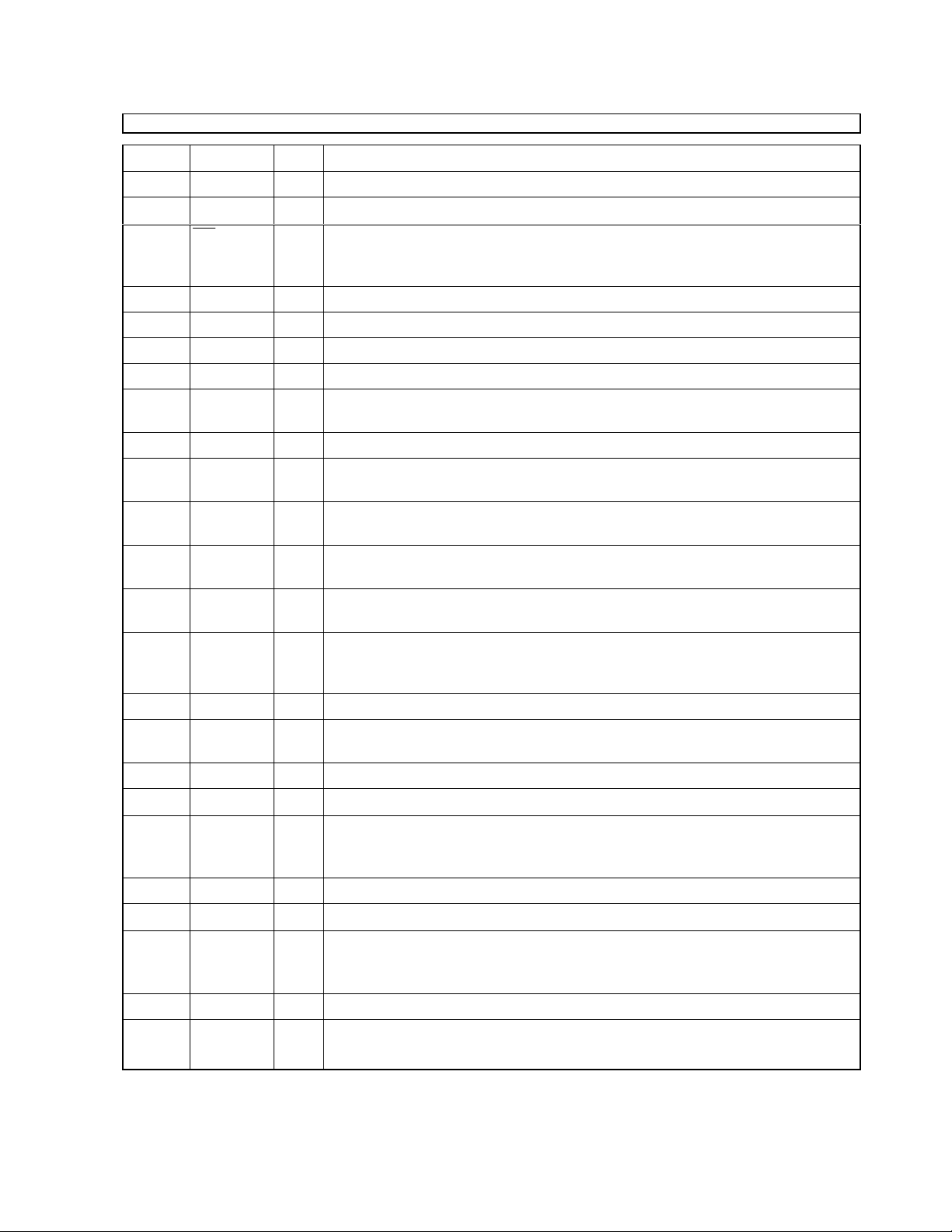
ABSOLUTE MAXIMUM RATINGS
(AVSS,DVSS=0V; Note 1 )
Parameter Symbol min max Units
Power Supplies: Analog
Digital
DADD-AVDD
AVDD
DVDD
VDA
-0.3
-0.3
Input Current, Any Pin Except Supplies IIN -
6.0
6.0
-
0.3
±
10
V
V
V
mA
Input Voltage VIND -0.3 A VDD+0.3 V
Ambient Operating Temperature Ta -40 85
Storage Temperature Tstg -65 150
C
°
C
°
Note: 1 . All voltages with respect to g r ound.
WA R NI NG: Operation at or be yond these limits may result in permanent damage to the devi ce.
Normal operation is not guaranteed at these extremes.
RECOMMENDED OPERATING CONDITIONS
(AVSS,DVSS=0V; Note 1 )
Parameter Symbol min typ max Units
Power Supplies: Analog (Note 2 )
Digital
AVDD
DVDD
4.5
4.5
5.0
5.0
5.5
AVDD
Voltage Reference (Note 3 ) VREF 2.5 - AVDD V
Notes: 2. AVDD and DVDD should be powered at the same t ime or AVDD should be powered earlier
than DVDD.
3. Analog output vo lt age scales with the voltage of VREF.
AOUT(typ.@0dB)=2.8Vpp*VREF/5.
* AKM assumes no responsibility for the usage beyond the conditions in t his data sheet.
V
V
0172-E-01 1997/5
- 4 -
ASAHI KASEI [AK4317]
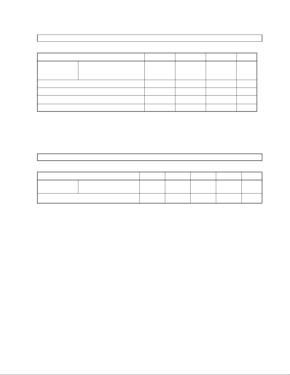
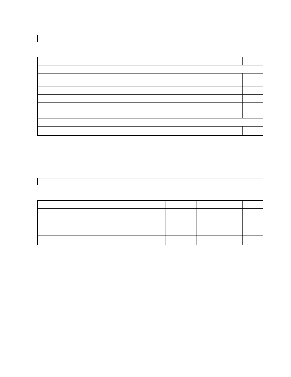
ANALOG CHARACTERISTICS
(Ta=25°C; AVDD,DVDD=5.0V; VREF=AVDD; fs=44.1kHz; Signal Frequency=1kHz; 18bit Input Data;
Measurement Bandwidth=10Hz∼20kHz; R
10kΩ; unless otherwise specified)
L
≥
Par ameter min typ max Units
Resolution 18 Bits
Dynamic Characteristics (Note 4 )
THD+N (0dB Output) -80 -86 dB
Dynamic Range (-60dB Output, A weight) 88 92 dB
S/N (A weight) 88 92 dB
Interchannel Isolation(1kHz) 80 90 dB
DC Accuracy
Interchannel Gain Mismatch 0.15 0.3 dB
Gain Drift (Note 5 ) 20 -
ppm/°C
DC Accuracy
Output Voltage (Note 6 ) 2.66 2.8 2.94 Vpp
Load Resistance 10
k
Ω
Power Supplies
Power Sup ply Current
Normal Operation (PD="H")
AVDD
DVDD
12
4
18
6
mA
mA
Power- Down-Mode (PD="L")
AVDD+DVDD (Note 7 )
10
50
uA
Power Dissipation (AVDD+D VDD)
Normal Operation
Power-Down-Mode (Note 7 )
80
50
120 mW
uW
Power Supply Rejection (Note 8 ) 50 dB
Notes: 4. Measured by AD725 C(SHIBASOKU). Averaging mode. Refer to the eva board manual.
5. The voltage o n VREF pin is held +5V ext e rnally.
6. Full-scale vo lt age(0dB). Output voltage scales with the voltage of VREF pin.
AOUT(typ.@0dB)=2.8Vpp*VREF/5.
7. Power Dissipation in t he power-do wn mode is applied with no external clocks
(MCLK,BICK,LRCK held "H" or "L").
8. PSR is applied to AVDD,DVDD with 1kHz, 100mVpp . VREF pin is held +5V.
0172-E-01 1997/5
- 5 -
ASAHI KASEI [AK4317]
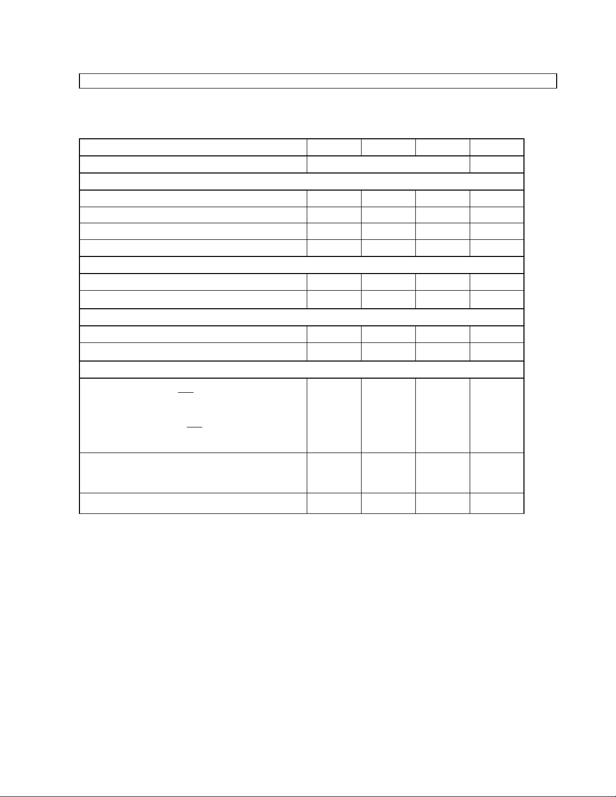
FILTER CHARA CTERISTICS
(Ta=25°C; AVDD,DVDD=4.5V∼5.5V; fs=44.1kHz; DE M="0")
Para meter Symbol min typ max Units
Digital Filter
Passband ±0.1dB (Note 9 )
-6.0dB
PB 0
- 22.05
20.0
-
kHz
kHz
Stopband (Note 9 ) SB 24.1 kHz
0.06
Passband Ripple PR
±
dB
Stopband Attenuation SA 43 dB
Group Delay (Note 10 ) G D - 14.7 - 1/fs
Digital Filter + SCF + CTF
0.5
Frequen cy Response 0∼20.0kHz
-
±
-dB
Note: 9. The passband and stopband frequencies scale with fs.
For examp le, P B=0.4535*fs(@±0.1dB), SB=0.546*fs.
10. The calc ulating delay t ime which occurred b y digital filtering. This time is from setting the
16/18bit data of both channels to input register to the output of anal og signal.
DIGITAL CHARACTERISTICS
(Ta=25°C; AVDD,DVDD=4.5∼5.5V)
Parameter Symbol min typ max Units
High-Level Input Voltage
Low-Le vel Input Voltage
High-Level Output Voltage (Iout=-100A)
Low-Le vel Output Voltage (Iout=100A)
VIH
VIL
VOH
VOL
2.2
-
DVDD-0.5
-
-
-
--
Input Leakage Current (Note 11 ) Iin - -
Notes: 11. DIF0,DIF1,DEM,TST1 pins have internal pull-do wn devices, nominally 160kΩ.
-
0.8
0.5
10 uA
±
V
V
V
V
0172-E-01 1997/5
- 6 -
 Loading...