

ASAHI KASEI [AK4309B]
AK4309B
16Bit SCF DAC for Multimedia
General Description
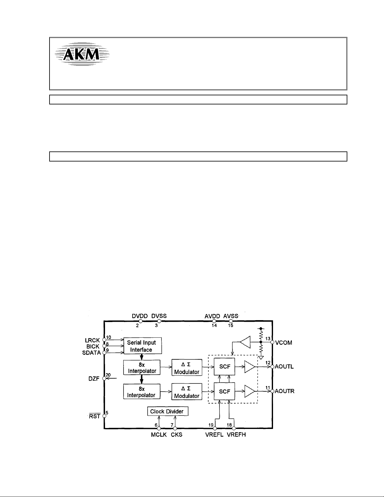
The AK4309B is a 1bit stereo DAC for multimedia audio systems. A 1bit DAC can achieve monotonicity and
low distortion with no adjustment and is superior to traditional R-2R ladder based DACs. In the AK4309B, the
loss of accuracy from clock jitter is also improved by using SCF techniques for on-chip post filter. The
AK4309B includes continuous time filter with single end output and does not need any external parts. The
master clock can be either 256fs or 384fs, supporting various audio environment.
Features
Sampling Rate Ranging from 8kHz to 50kHz
On chip Perfect filtering
•
8 times FIR Interpolator
•
2nd order SCF and CTF
•
Total Response: ±0.5dB at 20kHz
On chip Buffer with Single End Output
Master Clock: 256fs or 384fs
High Tolerance to Clock Jitter
TTL Level Digital Interface
THD+N: -84dB
Dynamic Range: 90dB
Output Level: 3.4Vpp
Power Supply: 5V±10%
Low Power Dissipation: 80mW at 5V
Small Package: 20pin SSOP
Pin Compatible with AK4310/4309A
0177-E-00 1997/6
- 1 -
ASAHI KASEI [AK4309B]
Ordering Guide
C
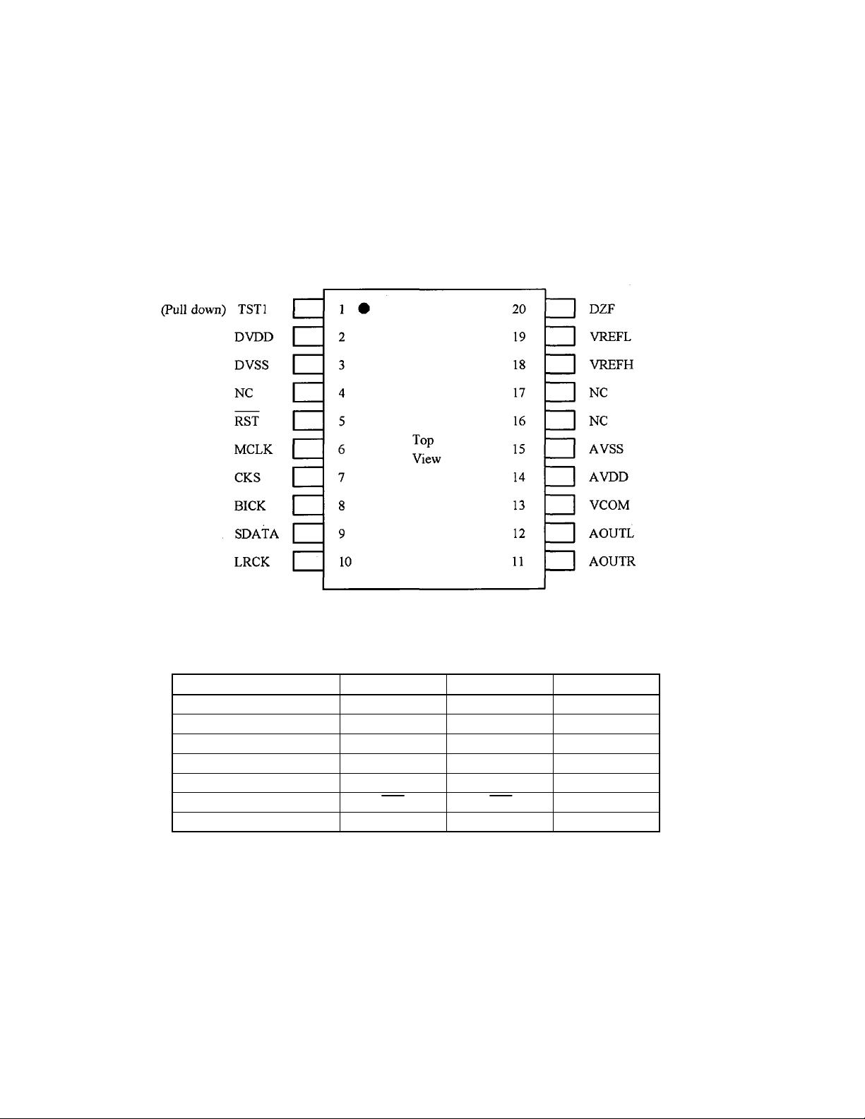
Pin Layout
AK4309BVM -10
AKD4309B Evaluation Board
+70
∼
°
(AK4309B's board is the same as AK4310's)
20pin SSOP(0.65mm pitch)
Compatibility with AK4310/09A
Parameter AK4310 AK4309A AK4309B
Power Supply
Digital I/F level CMOS TTL TTL
DR 92dB 91dB 90dB
Output Voltage 2.8Vpp 3.4Vpp 3.4Vpp
Click Noise High Middle Low
Function of Pin 4
Package 24SSOP 24SSOP 20SSOP
5.5V 4.5∼5.5V 4.5∼5.5V
3
∼
PD PD
NC
0177-E-00 1997/6
- 2 -
ASAHI KASEI [AK4309B]
PIN/FUNCTION
No. Pin Name I/O Function
1 TST1 I Test Pin (Pull-down pin)
Must be left floating or tied to DVSS.
2 DVDD - Digital Power Supply Pin
3 DVSS - Digital Ground Pin
4 NC - No Connection
RST
5
6 MCLK I Master Clock Input Pin
7 CKS I Master Clock Select Pin
8 BICK I Serial Bit Input Clock Pin
9 SDATA I Serial Data Input Pin
10 LRCK I L/R Clock Pin
11 AOUTR O Rch analog output pin
12 AOUTL O Lch analog output pin
13 VCOM O Common Voltage pin, AVDD/2
14 AVDD - Analog Po wer Supply Pin
15 AVSS - Analog Ground Pin
1617 NC
NC
18 VREFH I "H" Voltage Reference Input Pin
19 VREFL I "L" Voltage Reference Input Pin
20 DZF O Zero Input Detect Pin
* NC pins are not bonded internally.
I Reset Pin
When at "L", the AK4309B is in power-down mode and is held in reset.
The AK4309B should always be reset upon power-up.
An external TTL clock should be input on this pin.
The fs is selected by CKS pin.
"L": MCLK=256fs, "H": MCLK=384fs
This clock is used to latch SDATA.
2's complement MSB-first data is input on this pin.
This input determines which channel is currently being input on the Serial
Data Input pin, SDATA. "H": Lch, "L": Rch
Normally connected to AVSS with a 0.1uF ceramic capacitor in parallel with
a 10uF electrolytic cap.
- No Connection
The differential Voltage between VREFH and VREFL inputs set the analog
output range. The VREFH pin is normally connected to AVDD and the
VREFL pin is connected to AVSS. A 0.1uF ceramic capacitor should be as
near to both pins.
When SDATA of both channels follow a total 8192 LRCK cycles with "0"
input data, this pin goes "H".
0177-E-00 1997/6
- 3 -

ASAHI KASEI [AK4309B]
ABSOLUTE MAXIMUM RATINGS
(AVSS,DVSS=0V; Note 1 )
Parameter Symbol min max Units
Power Supplies: Analog
Digital
DVDD-AVDD
Input Current, Any Pin Except Supplies IIN Input Voltage VIND -0.3 AVDD+0.3 V
Ambient Operating Temperature Ta -10 70
Storage Temperature Tstg -65 150
Note: 1 . All voltages with respect to ground.
WARNING: Operation at or beyond these limits may result in permanent damage to the device.
Normal operation is not guaranteed at these extremes.
RECOMMENDED OPERATING CONDITIONS
AVDD
DVDD
VDA
-0.3
-0.3
-
6.0
6.0
0.3
±
10
V
V
V
mA
C
°
C
°
(AVSS,DVSS=0V; Note 1 )
Parameter Symbol min typ max Units
Power Supplies: Analog (Note 2 )
Digital
Voltage Reference(VREFH) (Note 3 ) VREF 3.0 - AVDD V
Notes: 2 . A VDD and DVDD should be powered at the same time or A VDD should be p owered earlier than DVDD.
3 . Analog output voltage scales with the voltage of VREFH at VREFL=AVSS.
AOUT(typ.@0dB)=3.4Vpp*VREFH/5.
* AKM assumes no responsibility for the usage beyond the conditions in this data sheet.
AVDD
DVDD
4.5
4.5
5.0
5.0
5.5
AVDD
V
V
0177-E-00 1997/6
- 4 -
ASAHI KASEI [AK4309B]
ANALOG CHARACTERISTICS
(Ta=25
Measurement Bandwidth=10Hz
Resolution 16 Bits
Dynamic Characteristics (Note 4 )
THD+N (0dB Output) -84 -79 dB
Dynamic Range (-60dB Output, A weight) 85 90 dB
S/N (A weight) 85 90 dB
Interchannel Isolation(1kHz) 80 90 dB
DC Accuracy
Interchannel Gain Mismatch 0.15 0.3 dB
Gain Drift (Note 5 ) 60 DC Accuracy
Output Voltage (Note 6 ) 3.23 3.4 3.57 Vpp
Load Resistance 10
Power Supplies
Power Supply Current
Normal Operation ( RST
AVDD
DVDD
Power-Down-Mode ( RST = "L")
AVDD+DVDD (Note 7 )
Power Dissipation (AVDD+DVDD)
Normal Operation
Power-Down-Mode (Note 7 )
Power Supply Rejection (Note 8 ) 50 dB
Notes: 4 . Measured by AD725C(SHIBASOKU). Averaging mode. Refer to the eva board manual.
5 . The voltage on VREFH pin is held +5V externally.
6 . Full-scale voltage(0dB). Output voltage scales with the voltage of VREH-VREFL.
AOUT(typ.@0dB)=3.4Vpp*(VREFH-VREFL)/5.
7 . Power Dissipation in the power-down mode is applied with no external clocks
(MCLK,BICK,LRCK held "H" or "L").
8 . PSR is applied to AVDD,DVDD with 1kHz, 100mVpp. VREF pin is held +5V.
C
; AVDD,DVDD=5.0V; VREFH=AVDD, VREF L= AVSS; fs=44.1kHz; Signal Frequency=1kHz;
°
20kHz; R
∼
Parameter min typ max Units
= "H")
L
10kΩ; unless otherwise specified)
≥
13
3
10
80
50
18
5
50
115
250
ppm/
k
Ω
mA
mA
uA
mW
uW
C
°
0177-E-00 1997/6
- 5 -

ASAHI KASEI [AK4309B]
FILTER CHARACTERISTICS
(Ta=25
Digital Filter
Passband -0.2dB (Note 9 )
-6.0dB
Stopband (Note 9 ) SB 24.3 kHz
Passband Ripple PR
Stopband Attenuation SA 41 dB
Group Delay (Note 10 ) GD - 14.5 - 1/fs
Digital Filter + SCF + CTF
Frequency Response 0∼20.0kHz
Note: 9 . The passband and stopband frequencies scale with fs.
(Ta=25
High-Level Input Voltage
Low-Level Input Voltage
High-Level Output Voltage (Iout=-100A)
Low-Level Output Voltage (Iout=100A)
Input Leakage Current Iin - -
C
; AVDD,DVDD=4.5V∼5.5V; fs=44.1kHz)
°
Parameter Symbol min typ max Units
PB 0
- 22.05
0.5
2.2
-
-
±
-
-
--
-
For example, PB=0.4535*fs(@-0.2dB), SB=0.55*fs.
10 . The calculating delay time which occurred by digital filtering. This time is from setting the 16bit
data of both channels to input register to the output of analog signal.
DIGITAL CHARACTERISTICS
C
; AVDD,DVDD=4.5∼5.5V)
°
Parameter Symbol min typ max Units
VIH
VIL
VOH
VOL
DVDD-0.5
20.0
-
0.05
±
-dB
-
0.8
0.5
10
±
kHz
kHz
dB
V
V
V
V
uA
0177-E-00 1997/6
- 6 -

ASAHI KASEI [AK4309B]
SWITCHING CHARACTERISTICS
(Ta=25
Master Clock Timing 256fs:
Pulse Width Low
Pulse Width High
384fs:
Pulse Width Low
Pulse Width High
LRCK
Frequency
Duty Cycle
Serial Interface Timing
BICK Period
BICK Pulse Width Low
Pulse Width High
BICK rising to LRCK edge (Note 11 )
LRCK Edge to BICK rising (Note 11 )
SDATA Hold Time
SDATA Setup Time
Reset Timing
RST Pulse Width (Note 12 ) tRST 150 ns
Notes: 11 .BICK rising edge must not occur at the same time as LRCK edge.
C
; AVDD,DVDD=4.5∼5.5V; CL=20pF)
°
Parameter Symbol min typ max Unit
fCLK
tCLKL
tCLKH
fCLK
tCLKL
tCLKH
fs
Duty
tBCK
tBCKL
tBCKH
tBLR
tLRB
tSDH
tSDS
12 .The AK4309B can be reset by bringing RST "L" to "H" only upon power up.
2.048
28
28
3.072
23
23
8
45
312.5
100
100
50
50
50
50
44.1 50
12.8
19.2
55
MHz
ns
ns
MHz
ns
ns
kHz
kHz
%
ns
ns
ns
ns
ns
ns
ns
0177-E-00 1997/6
- 7 -

ASAHI KASEI [AK4309B]
Timing Diagram
0177-E-00 1997/6
- 8 -

ASAHI KASEI [AK4309B]
OPERATION OVERVIEW
System Clock
The external clocks which are required to operate the AK4309B are MCLK, LRCK, BICK. The master
clock(MCLK) should be synchronized with LRCK but the phase is not critical. The MCLK is used to operate the
digital interpolation filter and the delta-sigma modulator. The frequency of MCLK is determined by the
sampling rate (LRCK), CKS pin. Table 1 illustrates corresponding clock frequencies. When the 384fs is
selected, the internal master clock becomes 256fs(=384fs*2/3). Refer to Figure 1 .
All external clocks(MCLK,BICK,LRCK) should always be present whenever the AK4309B is in normal
operation mode(RST="H"). If these clocks are not provided, the AK4309B may draw excess current because
the device utilizes dynamic refreshed logic internally. If the external clocks are not present, the AK4309B
should be in the power-down mode(RST ="L"). After exiting reset at power-up etc., the AK4309B is in powerdown mode until MCLK and LRCK are input.
Clock frequency
50kHz
8k
LRCK (fs)
BICK
MCLK
CKS="L" 256fs
CKS="H" 384fs
Table 1 . System Clocks
∼
∼
64fs
Figure 1 . MCLK divider
Audio Serial Interface Format
Data is shifted in via the SDATA pin using BICK and LRCK inputs. A serial data is MSB-first, 2's compliment
format and is latched by the rising edge of BICK.
Figure 2 . Data Input Timing
0177-E-00 1997/6
- 9 -

ASAHI KASEI [AK4309B]
Zero detection
When the input data at both channels are continuously zeros for 8192 LRCK cycles, DZF goes to "H". DZF
immediately goes "L" if input data are not zero after going DZF "H".
System Reset
The AK4309B should be reset once by bringing RST "L" upon power-up. The AK4309B is powered up and the
internal timing starts clocking by LRCK "
in power-down mode until LRCK is input.
Figure 3 shows the system connection diagram. An evaluation board[AKD4310] is available which
demonstrates the optimum layout, power supply arrangements and measurement results.
" after exiting reset and power down state by MCLK. The AK4309B is
↑
SYSTEM DESIGN
Figure 3 . Typical Connection Diagram
Notes:
- LRCK=fs, BICK
- Power lines of AVDD and D VDD should be distributed separately from the point
with low impedance of regulator etc.
- When AOUT drives some capacitive load, some resistor should be added
in series between AOUT and capacitive load.
- The capacitor value on VCOM depends on low frequency noise level of power supply.
0177-E-00 1997/6
32fs, MCLK=256fs at CKS="L", MCLK=384fs at CKS="H".
≥
- 10 -

ASAHI KASEI [AK4309B]
1. Grounding and Power Supply Decoupling
To minimize coupling by digital noise, decoupling capacitors should be connected to AVDD and DVDD,
respectively. AVDD is supplied from analog supply in system and DVDD is supplied from AVDD via 10
resistor as shown in Figure 3 . Alternatively if AVDD and DVDD are supplied separately, AVDD and DVDD
should be powered at the same time or AVDD should be powered earlier than DVDD. Analog ground and
digital ground should be connected together near to where the supplies are brought onto the printed circuit
board. Decoupling capacitors for high frequency should be placed as near as possible.
2. Voltage reference
The differential Voltage between VREFH and VREFL set the analog output range. VREFH pin is normally
connected to AVDD and VREFL pin is connected to AVSS with a 0.1uF ceramic capacitor. VCOM is a signal
ground of this chip. An electrolytic capacitor of around 10uF in parallel with a 0.1uF ceramic capacitor attached
to these pins eliminates the effects of high frequency noise. No load current may be drawn from VCOM pin. All
signals, especially clocks, should be kept away from the VREF and VCOM pins in order to avoid unwanted
coupling into the AK4309B.
3. Analog Outputs
Ω
The analog outputs are also single-ended and centered around the VCOM voltage. The output signal range is
typically 3.4Vpp. AC coupling capacitors of larger than 1uF are recommended. The internal switched-capacitor
filter and continuous-time filter attenuate the noise generated by the delta-sigma modulator beyond the audio
passband. Therefore, any external filters are not required for typical application. The output voltage is a
positive full scale for 7FFFH(@16bit) and a negative full scale for 8000H(@16bit). The ideal output is VCOM
voltage for 0000H(@16bit).
DC offsets on analog outputs are eliminated by AC coupling since analog outputs have DC offsets of VCOM +
a few mV.
0177-E-00 1997/6
- 11 -

ASAHI KASEI [AK4309B]
PACKAGE
zzzz
20pin SSOP (Unit: mm)
NOTE: Dimension “*” does not include mold flash.
Package & Lead frame material
Package molding compound : Epoxy
Lead frame material : Cu
Lead frame surface treatment : Solder plate
0177-E-00 1997/6
- 12 -

ASAHI KASEI [AK4309B]
MARKING
Contents of AAXXXX
AA: Lot#
XXXX: Date Code
0177-E-00 1997/6
- 13 -

IMPORTANT NOTICE
z These products and their specifications are subject to change without notice. Before
considering any use or application, consult the Asahi Kasei Microsystems Co., Ltd. (AKM)
sales office or authorized distributor concerning their current status.
z AKM assumes no liability for infringement of any patent, intellectual property, or other
right in the application or use of any information contained herein.
z Any export of these products, or devices or systems containing them, may require an
export license or other official approval under the l aw and regulations o f the country of
export pertaining to customs and tariffs, currency exchange, or strategic materials.
z AKM products are n either intended nor authorized for use as critical co mponents in any
safety, life support, or other hazard related device or system, and AKM assumes no
responsibility relating to any such use, except with the express written consent of the
Representative Director of AKM. As used here:
(a) A hazard related device or system is one designed or intended for life support or
maintenance of safety or for applications in medicine, aerospace, nuclear ener gy, or
other fields, in which its failure to function or perf orm may reasonably be expected to
result in loss of life or in significant injury or damage to person or property.
(b) A cr itical component is one whose fa ilure to function or per form may reasonably be
expected to result, whether directly or indirectly, in the loss of the safety or
effectiveness of the device or system containing it, and which must therefore meet
very high standards of performance and reliability.
z It is the responsibility of the buyer or distributor of an AKM product who distributes,
disposes of, or otherwise places the product with a third party to notify that party in
advance of the above content and conditions, and the buyer or distributor agrees to
assume any and all r esponsibility and liability for and ho ld AKM harmless from any and
all claims arising from the use of said product in the absence of such notification.
 Loading...