

AKM AK2548 Datasheet
ASAHI KASEI [AK2548]
R /W (WR)
MCLK
AS(ALE)
RCLK1
RPOS
RNEG1
LOS1
DS(RD)
TEST1-4
TNEG1
TPOS
TCLK1
AD7-AD0
RESET
CS
BTS
CLKSEL
P/S
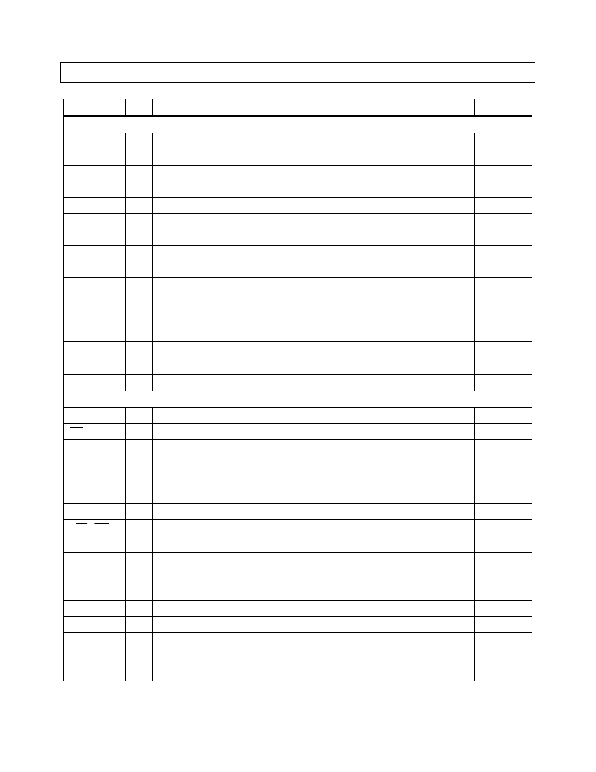
AK2548
7 channel E1 Transceiver
FEATURE
• 7ch E1 transceiver
• Jitter Tolerance: Compliant with ITU-T G.823, I.431
• Transmitter Pulse Shape: Compliant with ITU-T G.703
• Loss of Signal Detection: Compliant with ITU-T G.775
• Return loss: Compliant with ETS 300 166
• Selectable Signal Polarity
• Local/Remote Loopback
• Parallel/Serial Microprocessor Interface
• Single 3.3V±5% Operation
• Low Power Consumption
• Pin-to-pin compatible with AK2546(7 channel T1 transceiver) except serial interface
• Small Plastic Package 144pin LQFP
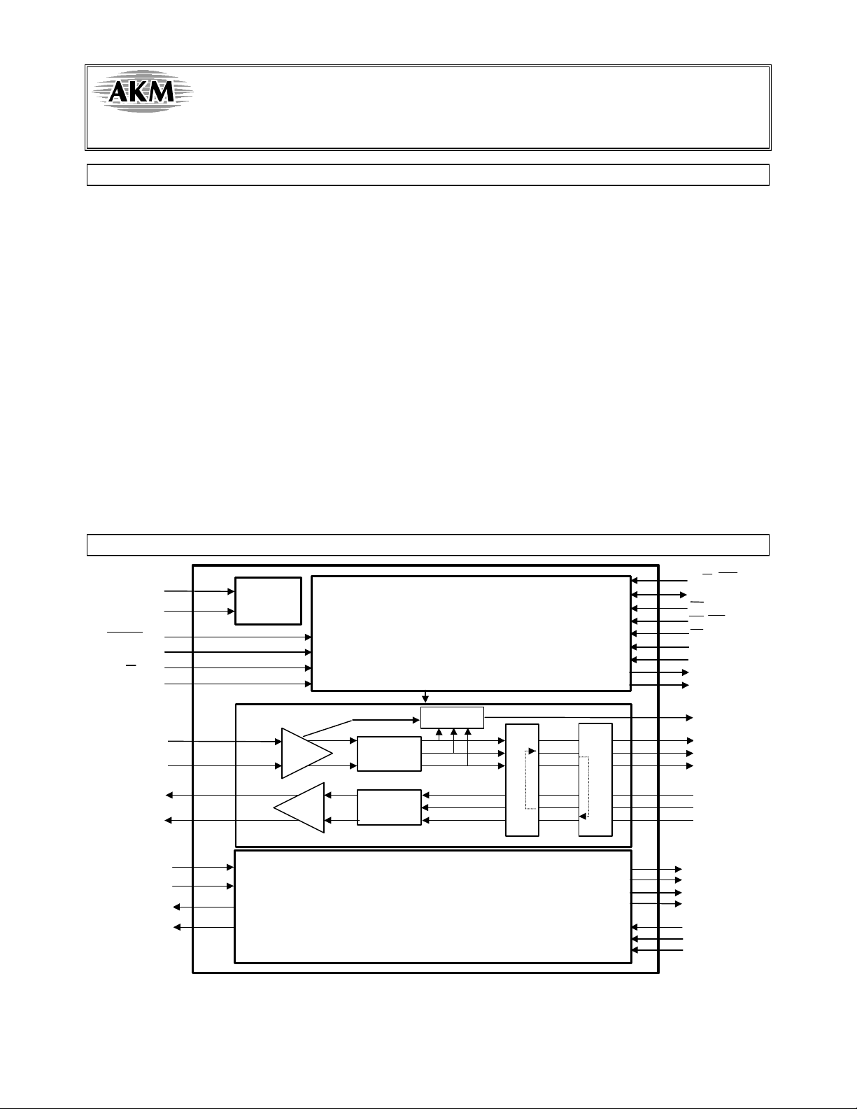
CLKGEN
TRANSCEIVER 1
RTIP1
RRING1
TTIP1
TRING1
RTIP2-7
RRING2-7
TTIP2-7
TRING2-7
TRANSCEIVER 2-7
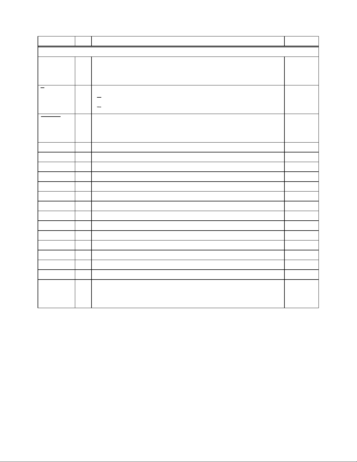
BLOCK DIAGRAM
CONTROL
LOS
RECOVER
SHAPER
Local Loopback
SCLK
SDI
SDO
INT
Remote Loopback
LOS2-7
RCLK2-7
RPOS2-7
RNEG2-7
TCLK2-7
TPOS2-7
TNEG2-7
7 Channel E1 Transceiver Block Diagram
ASAHI KASEI [AK2548]
AD7/SDO
73
144
143
142
141
140
139
138
137
136
135
134
133
132
131
130
129
128
127
126
125
124
123
122
121
120
119
118
117
116
115
114
113
112
111
110
109
36
72
/SDI
RRING7
BTS
RRING6
TEST4
RRING5
TEST3
TEST2
RRING4
RRING3
RRING2
TEST1
RRING1
GENERAL DESCRIPTION
The AK2548 is the 7 channel E1 transceiver for a SDH/SONET MUX, M13 MUX, etc.
It includes seven independent transmitters, clock and data recovery, LOS detector, control circuit
in one LQFP-144 package which saves space, power consumption and the board design time.
Internally generated transmit pulse provides the appropriate pulse shape.
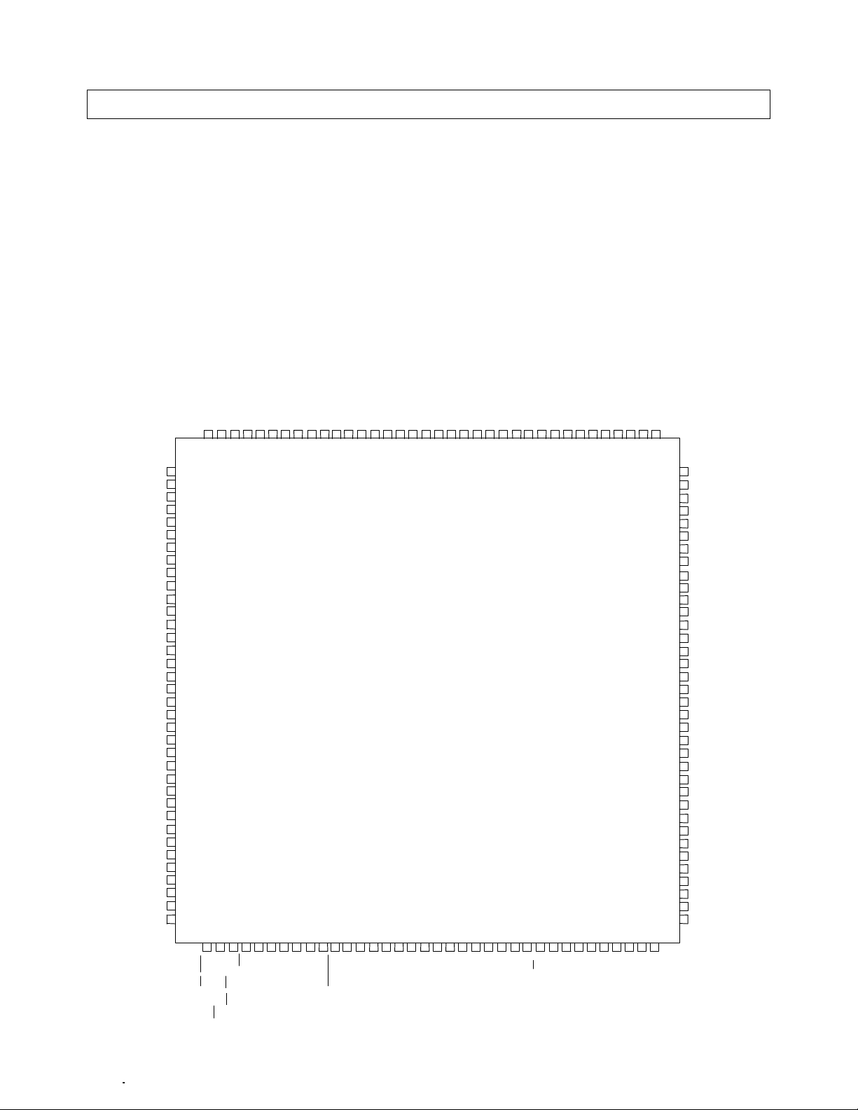
PIN ASSIGNMENTS
AVSS8
TTIP7
TVSS7
TVDD7
TRING7
AVSS7
TTIP6
TVSS6
TVDD6
TRING6
AVSS6
TTIP5
TVSS5
TVDD5
TRING5
AVSS5
TTIP4
TVSS4
TVDD4
TRING4
AVSS4
TTIP3
TVSS3
TVDD3
TRING3
AVSS3
TTIP2
TVSS2
TVDD2
TRING2
AVSS2
TTIP1
TVSS1
TVDD1
TRING1
AVSS1
TCLK7
TPOS7
TNEG7
RCLK7
RPOS7
RNEG7
TCLK6
TPOS6
TNEG6
RCLK6
RPOS6
RNEG6
IOVDD2
IOVSS2
TAVDD2
TAVSS2
TCLK5
TPOS5
TNEG5
RCLK5
RPOS5
RNEG5
DAVSS2
DVSS2
DVDD2
LOS7
LOS6
LOS5
AD0
AD1
AD2
AD3
AD4
AD5
AD6
1
2
3
4
5
6
7
8
9
10
11
12
13
14
15
16
17
18
19
20
21
22
23
24
25
26
27
28
29
30
31
32
33
34
35
3738394041424344454647484950515253545556575859606162636465666768697071
(TOP VIEW)
108
107
106
105
104
103
102
101
100
TCLK1
TPOS1
TNEG1
RCLK1
RPOS1
RNEG1
TCLK2
TPOS2
TNEG2
RCLK2
99
RPOS2
98
RNEG2
97
IOVDD1
96
IOVSS1
95
TAVDD1
94
TAVSS1
93
TCLK3
92
TPOS3
91
TNEG3
90
RCLK3
89
RPOS3
88
RNEG3
87
DAVSS1
86
DVSS1
85
DVDD1
84
TCLK4
83
TPOS4
82
TNEG4
81
RCLK4
80
RPOS4
79
RNEG4
78
LOS1
77
LOS2
76
LOS3
75
LOS4
74
RAVDD1
CS
INT
PVSS
MCLK
PVDD
RAVSS2
R/W(WR)
DS(RD)
AS(ALE)/SCLK
RESET
RAVDD2
RTIP7
RTIP6
RTIP5
BVSS
BVDD
BGREF
P/S
RTIP4
RTIP3
CLKSEL
RTIP2
RTIP1
RAVSS1
ASAHI KASEI [AK2548]
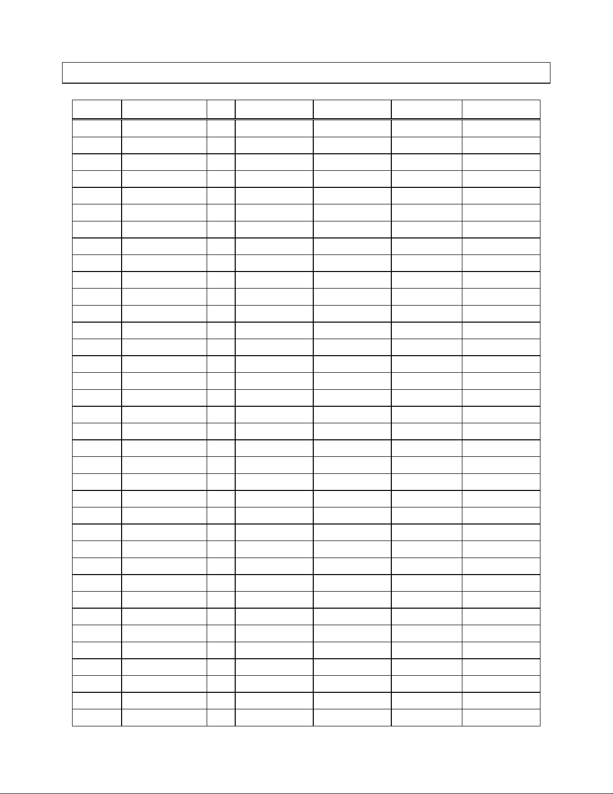
PIN CONDITION
Pin No. Pin Name I/O Pin Type AC Load DC Load Comments
1
2
3
4
5
6
7
8
9
10
11
12
13
14
15
16
17
18
19
20
21
22
23
24
25
26
27
28
29
30
31
32
33
34
35
36
TCLK7 I CMOS
TPOS7 I CMOS
TNEG7 I CMOS
RCLK7 O CMOS ≤15pF
RPOS7 O CMOS ≤15pF
RNEG7 O CMOS ≤15pF
TCLK6 I CMOS
TPOS6 I CMOS
TNEG6 I CMOS
RCLK6 O CMOS ≤15pF
RPOS6 O CMOS ≤15pF
RNEG6 O CMOS ≤15pF
IOVDD2 I Power
IOVSS2 I Power
TAVDD2 I Power
TAVSS2 I Power
TCLK5 I CMOS
TPOS5 I CMOS
TNEG5 I CMOS
RCLK5 O CMOS ≤15pF
RPOS5 O CMOS ≤15pF
RNEG5 O CMOS ≤15pF
DAVSS2 I Power
DVSS2 I Power
DVDD2 I Power
LOS7 O CMOS ≤15pF
LOS6 O CMOS ≤15pF
LOS5 O CMOS ≤15pF
AD0 I/O CMOS ≤50pF
AD1 I/O CMOS ≤50pF
AD2 I/O CMOS ≤50pF
AD3 I/O CMOS ≤50pF
AD4 I/O CMOS ≤50pF
AD5 I/O CMOS ≤50pF
AD6 I/O CMOS ≤50pF
AD7/SDO I/O CMOS ≤50pF

ASAHI KASEI [AK2548]
±
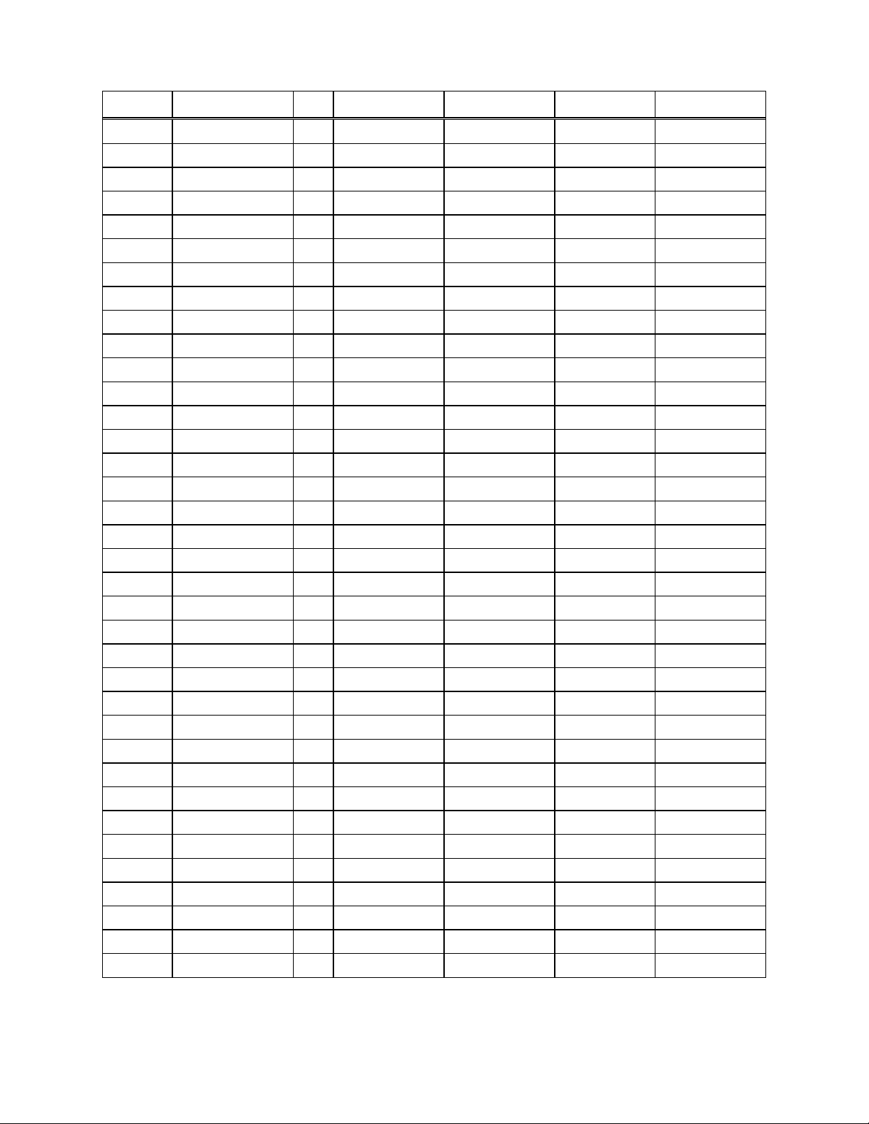
Pin No. Pin Name I/O Pin Type AC Load DC Load Comments
37
38
39
40
41
42
43
44
45
46
47
48
49
50
51
52
53
54
55
56
57
58
59
60
61
62
63
64
65
66
67
68
69
70
71
72
R/W(WR) I CMOS
AS(ALE)
/SCLK
I CMOS
DS(RD)/SDI I CMOS
CS I CMOS
INT O Open drain PMOS
open drain
PVDD I Power
MCLK I CMOS
PVSS I Power
RAVSS2 I Power
RAVDD2 I Power
RESET I CMOS
RRING7 I Analog
RTIP7 I Analog
BTS I CMOS
RRING6 I Analog
RTIP6 I Analog
TEST4 I CMOS Note 1
RRING5 I Analog
RTIP5 I Analog
TEST3 I CMOS Note 1
BVSS I Power
BGREF O Analog 12kΩ
1% accuracy
BVDD I Power
TEST2 I CMOS Note 1
RRING4 I Analog
RTIP4 I Analog
P/S I CMOS
RRING3 I Analog
RTIP3 I Analog
CLKSEL I CMOS
RRING2 I Analog
RTIP2 I Analog
TEST1 I CMOS Note 1
RRING1 I Analog
RTIP1 I Analog
RAVSS1 I Power

ASAHI KASEI [AK2548]
Pin No. Pin Name I/O Pin Type AC Load DC Load Comments
73
74
75
76
77
78
79
80
81
82
83
84
85
86
87
88
89
90
91
92
93
94
95
96
97
98
99
100
101
102
103
104
105
106
107
108
RAVDD1 I Power
LOS4 O CMOS ≤15pF
LOS3 O CMOS ≤15pF
LOS2 O CMOS ≤15pF
LOS1 O CMOS ≤15pF
RNEG4 O CMOS ≤15pF
RPOS4 O CMOS ≤15pF
RCLK4 O CMOS ≤15pF
TNEG4 I CMOS
TPOS4 I CMOS
TCLK4 I CMOS
DVDD1 I Power
DVSS1 I Power
DAVSS1 I Power
RNEG3 O CMOS ≤15pF
RPOS3 O CMOS ≤15pF
RCLK3 O CMOS ≤15pF
TNEG3 I CMOS
TPOS3 I CMOS
TCLK3 I CMOS
TAVSS1 I Power
TAVDD1 I Power
IOVSS1 I Power
IOVDD1 I Power
RNEG2 O CMOS ≤15pF
RPOS2 O CMOS ≤15pF
RCLK2 O CMOS ≤15pF
TNEG2 I CMOS
TPOS2 I CMOS
TCLK2 I CMOS
RNEG1 O CMOS ≤15pF
RPOS1 O CMOS ≤15pF
RCLK1 O CMOS ≤15pF
TNEG1 I CMOS
TPOS1 I CMOS
TCLK1 I CMOS
ASAHI KASEI [AK2548]
Pin No. Pin Name I/O Pin Type AC Load DC Load Comments
109
110
111
112
113
114
115
116
117
118
119
120
121
122
123
124
125
126
127
128
129
130
131
132
133
134
135
136
137
138
139
140
141
142
143
144
AVSS1 I Power
TRING1 O Analog driver output
TVDD1 I Power
TVSS1 I Power
TTIP1 O Analog driver output
AVSS2 I Power
TRING1 O Analog driver output
TVDD2 I Power
TVSS2 I Power
TTIP2 O Analog driver output
AVSS3 I Power
TRING3 O Analog driver output
TVDD3 I Power
TVSS3 I Power
TTIP3 O Analog driver output
AVSS4 I Power
TRING4 O Analog driver output
TVDD4 I Power
TVSS4 I Power
TTIP4 O Analog driver output
AVSS5 I Power
TRING5 O Analog driver output
TVDD5 I Power
TVSS5 I Power
TTIP5 O Analog driver output
AVSS6 I Power
TRING6 O Analog driver output
TVDD6 I Power
TVSS6 I Power
TTIP6 O Analog driver output
AVSS7 I Power
TRING7 O Analog driver output
TVDD7 I Power
TVSS7 I Power
TTIP7 O Analog driver output
AVSS8 I Power
Note 1)Should be connected to VSS externally.
ASAHI KASEI [AK2548]
PIN FUNCTION
Pin Name I/O Function Comment
E1 Transceiver
TTIP1-7
TRING1-7
TPOS1-7
TNEG1-7
TCLK1-7 I Transmit Clock Input
RTIP1-7
RRING1-7
RPOS1-7
RNEG1-7
RCLK1-7 O Receive Clock Output recovered from receive data input
LOS1-7 O Loss of signal output
TVDD1-7 Positive Power Supply for the Transmit Driver
TVSS1-7 Negative Power Supply for the Transmit Driver
AVSS1-8 Analog ground .
Common Block
MCLK I 2.048/32.768MHz External Reference Clock Input
AS(ALE) I Address Select(Address Latch Enable) Input
INT O Interrupt Output(PMOS open drain , should be tied to GND through
DS(RD) I Data Strobe(Read Enable) Input
R/W (WR) I Read/Write(Write Enable) Input
CS I Chip Select Input
BTS I Bus Type Select Input
SCLK I Serial Clock Input
SDI I Serial Data Input
SDO O Serial Data Output
AD0-AD7 I/O Address/Data Input/Output
OOTransmit Tip/Ring Output
Bipolar output over transmit transformer
IITransmit Positive/Negative Data Input
Input on the falling edge of TCLK
IIReceive Tip/Ring Input
Bipolar Input over receive transformer
OOReceive Positive/Negative Data Output
Output on the falling edge of RCLK
Output “high” when detect loss of signal
LOSx output is not masked by MLOSx register.
a resistor), Active High, INT output goes “high” when the alarm is
reported to any one of LOSx, LOTCx or LOMC registers. This pin can
be masked by MLOSx, MLOTCx or MLOMC registers.
BTS=“H” : Motorola Mode
BTS=“L” : Intel Mode
Used for read/write internal registers.
ASAHI KASEI [AK2548]
TEST1,2,3,4
Pin Name I/O Function Comment
Common Block
CLKSEL I MCLK Select Input
CLKSEL=“H”:2.048MHz
CLKSEL=“L”:34.768MHz
P/S I Parallel/Serial Port Select
P/S=“H”: Serial Port is selected
P/S=“L”: Parallel Port is selected
RESET I Reset Input
Active “Low” input pulse over 200ns initializes the internal circuit
and forces RPOSx/RNEGx output “low” and LOSx output “high”.
I Factory Use. Should be connected to VSS externally.
TAVDD1,2 Positive Power Supply for the analog circuitry in the transmitters
TAVSS1,2 Negative Power Supply for the analog circuitry in the transmitters
RAVDD1,2 Positive Power Supply for the analog circuitry in the receivers
RAVSS1,2 Negative Power Supply for the analog circuitry in the receivers
DVDD1,2 Positive Power Supply for Digital
DVSS1,2 Negative Power Supply for Digital
DAVSS1,2 Ground for Digital
IOVDD1,2 Positive Power Supply for I/O
IOVSS1,2 Negative Power Supply for I/O
BVDD Positive Power Supply for Reference Circuit
BVSS Negative Power Supply for Reference Circuit
PVDD Positive Power Supply for PLL
PVSS Negative Power Supply for PLL
BGREF Bandgap Reference Output.
12kΩ±1% exeternal register should be connected across this pin and
VSS.
ASAHI KASEI [AK2548]
ABSOLUTE MAXIMUM RATINGS
Parameter Symbol Min Typ Max Units Condition
DC Supply VDD -0.3 6.5 V
Input Voltage
Input Current IIN 10 mA
Storage Temperature Tstg -55 130 ºC
Note) All voltages with respect to ground.
All negative voltage pins=0V. VDD apply to all positive voltage pins.
VIN1 -0.3 VDD+0.3 V Apply to except for RTIPx,
RRINGx
VIN2 -3 VDD+0.3 V Apply to RTIPx, RRINGx
RECOMMENDED OPERATING CONDITIONS
Parameter Symbol min typ max Units Condition
DC Supply V+ 3.135 3.3 3.465 V 3.3V±5%
Ambient Operating Temperature Ta -40 25 +85 ºC
Note) All voltages with respect to ground.
All negative voltage pins=0V. VDD apply to all positive voltage pins.
ELECTORICAL CHARACTERISTICS
DC CHARACTERISTICS
Parameter Symbol min typ max Units Condition
Power Consumption(/ch) 75Ω
120Ω
Digital High-Level Output Voltage VOH 0.9VDD V IOH=-40µA
Digital Low-Level Output Voltage VOL 0.4 V IOL=500µA
Digital High-Level Input Voltage VIH 0.7VDD V
Digital Low-Level Input Voltage VIL 0.3VDD V
Input Leak Current Ii 10 µA
Output Current IOH 1.0 mA INT pin
Note1: typ: 50% mark, Room temp., VDD 3.3V
max: 100% mark, Temp./VDD in all range
Not include any other load(ex. External pull up register) except lines.
PD 75
70
160
147
mWmWNote1
 Loading...