

AKM AK2540 Datasheet

ASAHI KASEI [AK2540]
MCLK
RCLK1
RPOS1
RNEG1
LOS1
TNEG1
TPOS1
TCLK1
DFM
DFM1
TAOS
MCLKSEL
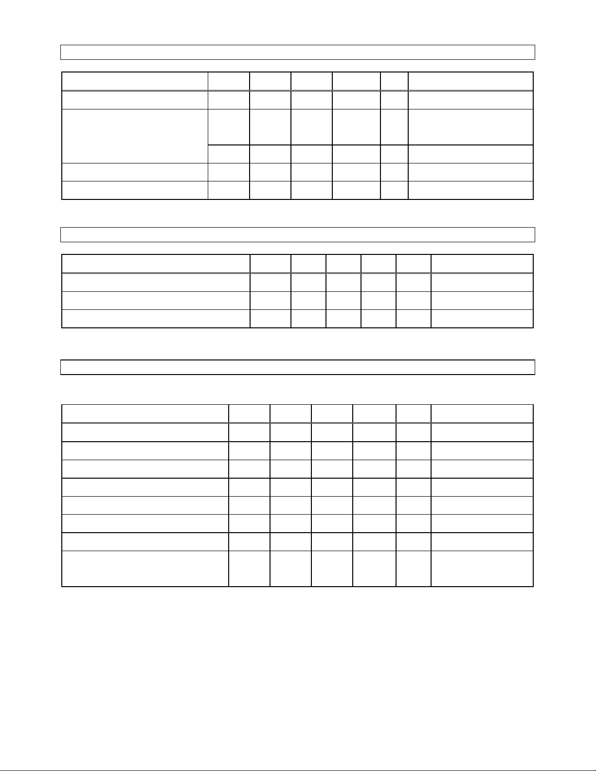
Quad T1 Transceiver
FEATURE
- 4ch short haul T1 transceiver with jitter attenuator
- Jitter Tolerance: Compliant with GR-499 Category I,II and TR 62411
- Transmitter Pulse Shape: Compliant with GR-499 and ANSI T1.102 (1993)
- Loss of Signal Detection
- Local/Remote Loopback Mode
- Driver Failure Monitor
- Current limiter in transmit drivers for short circuits protection
- Hardware/Host Control Mode
- Single 3.3V±5% or 5.0V±5% Operation
- Low Power Consumption
- Package: 144LQFP
AK2540
RCLK2-4
RPOS2-4
RNEG2-4
TCLK2-4
TPOS2-4
TNEG2-4
TRANSCEIVER 1
JITTER
ATT
Remote Loopback
TRANSCEIVER 2-4
BLOCK DIAGRAM
CLOCK
&DATA
Local Loopback
RECOVERY
LOS
PULSE
SHAPER
TTIP1
TRING1
RTIP1
RRING1
DFM2-4
TTIP2-4
TRING2-4
RTIP2-4
RRING2-4
LOS2-4
CONTROL
CLKGEN
Quad T1 Transceiver Block Diagram
ASAHI KASEI [AK2540]
73
144
143
142
141
140
139
138
137
136
135
134
133
132
131
130
129
128
127
126
125
124
123
122
121
120
119
118
117
116
115
114
113
112
111
110
109
36
72
AD7_LENG13
NC
_LENG03
_LENG24
_LENG14
CS_LENG04
BTS_AIS1SEL
HWMODE
SEL5V
CLKE
TEST8
RRING4
RTIP4
TEST7
TEST6
RRING3
RTIP3
TEST5
PVSS
NC
MCLK
MCLKSEL
PVDD
BVDD
BVSS
TEST4
RRING2
RTIP2
TEST3
TEST2
RRING1
RTIP1
TEST1
NC
GENERAL DESCRIPTIONS
The AK2540 is the quad short haul T1 transceiver for asynchronous applications, such as M13
MUX, etc. It includes Transmitter, Clock and Data Recovery, Jitter Attenuator, LOS Detector,
Driver Failure Monitor, Control Circuits, etc. in one LQFP-144 package. Internally generated
transmit pulse provides the appropriate pulse shape for line length ranging from 0 to 655 feet from
a DSX-1 cross connect.
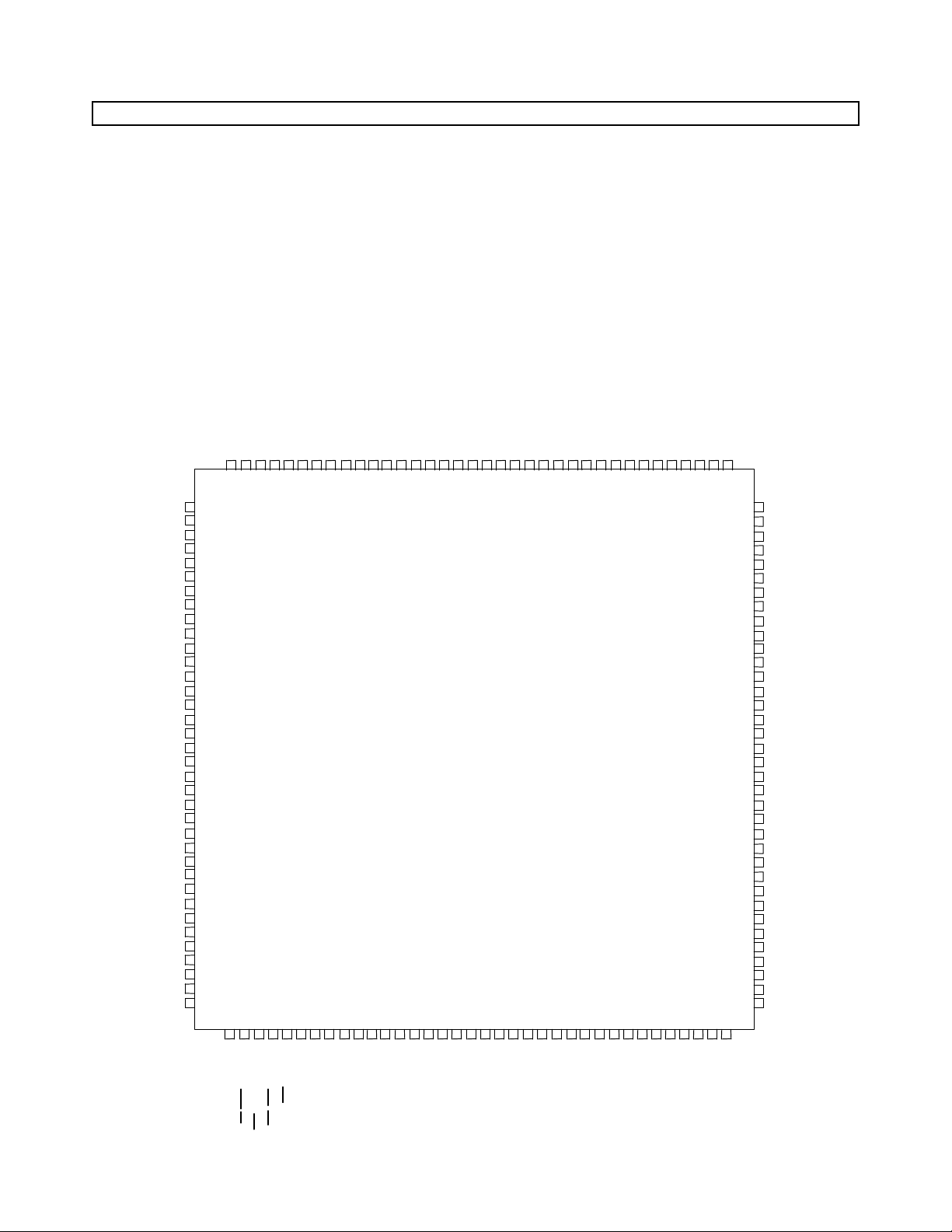
PIN ASSIGNMENTS
NCNCNC
LLOOP4
RLOOP4
TTIP4
TVSS4
TVDD4
TRING4
AVSS4NCLLOOP3
RLOOP3
TTIP3
TVSS3
TVDD3
TRING3
AVSS3NCLLOOP2
RLOOP2
TTIP2
TVSS2
TVDD2
TRING2
AVSS2NCNC
LLOOP1
RLOOP1
TTIP1
TVSS1
TVDD1
TRING1
AVSS1
NC
DFM3
AIS3
TPOS3
TNEG3
TCLK3
LOS3
RPOS3
RNEG3
NC
RCLK3
DFM4
AIS4
TAVDD1
NC
TAVSS1
TPOS4
TNEG4
TCLK4
LOS4
RPOS4
RNEG4
RCLK4
DAVSS2
NC
IOVDD
IOVSS
NC
NC
AD0_LENG21
AD1_LENG11
AD2_LENG01
AD3_LENG22
AD4_LENG12
AD5_LENG02
AD6_LENG23
1
2
3
4
5
6
7
8
9
10
11
12
13
14
15
16
17
18
19
20
21
22
23
24
25
26
27
28
29
30
31
32
33
34
35
3738394041424344454647484950515253545556575859606162636465666768697071
(TOP VIEW)
108
107
106
105
104
103
102
101
100
DFM1
AIS1
TPOS1
TNEG1
TCLK1
LOS1
RPOS1
RNEG1
NC
RCLK1
99
DFM2
98
AIS2
97
NC
96
NC
95
TAVDD2
94
TAVSS2
93
NC
92
DVSS
91
DVDD
90
DAVSS1
89
NC
88
TPOS2
87
TNEG2
86
TCLK2
85
NC
84
LOS2
83
RPOS2
82
RNEG2
81
RCLK2
80
NC
79
JASELT
78
JASELR
77
NC
76
RAVDD
75
RAVSS
74
NC
AS(ALE)
R/W(WR)
DS(RD)
INT_LOMC
RESET
BGREF
ASAHI KASEI [AK2540]
PIN CONDITION
Pin # Pin Name I/O Pin Type AC Load DC Load Comments
1
2
3
4
5
6
7
8
9
10
11
12
13
14
15
16
17
18
19
20
21
22
23
24
25
26
27
28
29
30
31
32
33
34
35
36
DFM3 O CMOS ≤15pF
AIS3 I CMOS Note2)
TPOS3 I CMOS
TNEG3 I CMOS
TCLK3 I CMOS
LOS3 O CMOS ≤15pF
RPOS3 O CMOS ≤15pF
RNEG3 O CMOS ≤15pF
NC
RCLK3 O CMOS ≤15pF
DFM4 O CMOS ≤15pF
AIS4 I CMOS Note2)
TAVDD1 I Power
NC
TAVSS1 I Power
TPOS4 I CMOS
TNEG4 I CMOS
TCLK4 I CMOS
LOS4 O CMOS ≤15pF
RPOS4 O CMOS ≤15pF
RNEG4 O CMOS ≤15pF
RCLK4 O CMOS ≤15pF
DAVSS2 I Power
NC
IOVDD I Power
IOVSS I Power
NC
NC
AD0_LENG21 I/O CMOS ≤50pF
AD1_LENG11 I/O CMOS ≤50pF
AD2_LENG01 I/O CMOS ≤50pF
AD3_LENG22 I/O CMOS ≤50pF
AD4_LENG12 I/O CMOS ≤50pF
AD5_LENG02 I/O CMOS ≤50pF
AD6_LENG23 I/O CMOS ≤50pF
AD7_LENG13 I/O CMOS ≤50pF

ASAHI KASEI [AK2540]
Pin # Pin Name I/O Pin Type AC Load DC Load Comments
37
38
39
40
41
42
43
44
45
46
47
48
49
50
51
52
53
54
55
56
57
58
59
60
61
62
63
64
65
66
67
68
69
70
71
72
NC
R/W(WR)_LENG03 I CMOS
AS(ALE)_LENG24 I CMOS
DS(RD)_LENG14 I CMOS
CS_LENG04 I CMOS
BTS_AIS1SEL I CMOS
INT_LOMC O Open drain PMOS
Open drain
HWMODE I CMOS
RESET I CMOS
SEL5V I CMOS
CLKE I CMOS
TEST8 I CMOS Note1)
RRING4 I Analog
RTIP4 I Analog
TESE7 I CMOS Note1)
TEST6 I CMOS Note1)
RRING3 I Analog
RTIP3 I Analog
TEST5 I CMOS Note1)
PVSS I Power
NC
MCLK I CMOS
MCLKSEL I CMOS
PVDD I Power
BVDD I Power
BGREF O Analog 12kΩ ±1% accuracy
BVSS I Power
TEST4 I CMOS Note1)
RRING2 I Analog
RTIP2 I Analog
TEST3 I CMOS Note1)
TEST2 I CMOS Note1)
RRING1 I Analog
RTIP1 I Analog
TEST1 I CMOS Note1)
NC

ASAHI KASEI [AK2540]
Pin # Pin Name I/O Pin Type AC Load DC Load Comments
73
74
75
76
77
78
79
80
81
82
83
84
85
86
87
88
89
90
91
92
93
94
95
96
97
98
99
100
101
102
103
104
105
106
107
108
NC
RAVSS I Power
RAVDD I Power
NC
JASELR I CMOS Note2)
JASELT I CMOS Note2)
NC
RCLK2 O CMOS ≤15pF
RNEG2 O CMOS ≤15pF
RPOS2 O CMOS ≤15pF
LOS2 I CMOS ≤15pF
NC
TCLK2 I CMOS
TNEG2 I CMOS
TPOS2 I CMOS
NC
DAVSS1 I Power
DVDD I Power
DVSS I Power
NC
TAVSS2 I Power
TAVDD2 I Power
NC
NC
AIS2 I CMOS Note2)
DFM2 O CMOS ≤15pF
RCLK1 O CMOS ≤15pF
NC
RNEG1 O CMOS ≤15pF
RPOS1 O CMOS ≤15pF
LOS1 O CMOS ≤15pF
TCLK1 I CMOS
TNEG1 I CMOS
TPOS1 I CMOS
AIS1 I CMOS Note2)
DFM1 O CMOS ≤15pF
ASAHI KASEI [AK2540]
Pin # Pin Name I/O Pin Type AC Load DC Load Comments
109
110
111
112
113
114
115
116
117
118
119
120
121
122
123
124
125
126
127
128
129
130
131
132
133
134
135
136
137
138
139
140
141
142
143
144
NC
AVSS1 I Power
TRING1 O Analog driver output
TVDD1 I Power
TVSS1 I Power
TTIP1 O Analog driver output
RLOOP1 I CMOS Note2)
LLOOP1 I CMOS Note2)
NC
NC
AVSS2 I Power
TRING2 O Analog driver output
TVDD2 I Power
TVSS2 I Power
TTIP2 O Analog driver output
RLOOP2 I CMOS Note2)
LLOOP2 I CMOS Note2)
NC
AVSS3 I Power
TRING3 O Analog driver output
TVDD3 I Power
TVSS3 I Power
TTIP3 O Analog driver output
RLOOP3 I CMOS Note2)
LLOOP3 I CMOS Note2)
NC
AVSS4 I Power
TRING4 O Analog driver output
TVDD4 I Power
TVSS4 I Power
TTIP4 O Analog driver output
RLOOP4 I CMOS Note2)
LLOOP4 I CMOS Note2)
NC
NC
NC
Note1 )Should be connected to VSS externally.
Note2 )Should be connected to VSS externally in host mode.
Note3 )All NC pins are recommended to connected to VSS externally.

ASAHI KASEI [AK2540]
PIN DESCRIPTIONS
Pin Name I/O Function Comments
T1 Transceiver
TTIP1-4
TRING1-4
TPOS1-4
TNEG1-4
TCLK1-4 I Transmit Clock Input pins
RTIP1-4
RRING1-4
RPOS1-4
RNEG1-4
RCLK1-4 O Receive Clock Output recovered from receive data input pins
RLOOP1-4 I Remote Loopback Control input pins Note1)
LLOOP1-4 I Local Loopback Control input pins Note1)
LENG01-04 I Line Length Control 0 input pins Note1)
LENG11-14 I Line Length Control 1 input pins Note1)
LENG21-24 I Line Length Control 2 input pins Note1)
AIS1-4 I Transmit AIS Enable input pins Note1)
AIS1SEL I Transmit All Ones/Zero Selection input pins when AIS is enabled Note1)
JASELR I Jitter Attenuator Select input pin, placed at Receiver Note1)
JASELT I Jitter Attenuator Select input pin, placed at Transmitter Note1)
DFM1-4 O Driver Failure Monitor output pins
LOS1-4 O Loss of signal output pins
TVDD1-4 Positive Power Supply for the Transmit Driver
TVSS1-4 Negative Power Supply for the Transmit Driver
AVSS1-4 Analog ground.
Common Block
OOTransmit Tip/Ring Output pins
Bipolar output over transmit transformer
IITransmit Positive/Negative Data Input pins
Input on the falling edge of TCLK
IIReceive Tip/Ring Input pins
Bipolar Input over receive transformer
OOReceive Positive/Negative Data Output pins
Output on the rising/falling edge of RCLK
(determined by CLKE pin)
Output “high” when detect loss of signal
LOSx output is not masked by MLOSx register.
MCLK I 1.544MHz or 24.704MHz External Reference Clock input pin
LOMC O Loss of master clock output pin.
Output “high” when detect loss of master clock
LOMC output is not masked by MLOMC register.
AS(ALE) I Address Select(Address Latch Enable) input pin Note2)
INT O Interrupt Output pin(PMOS open drain), Active High,
INT output goes “high” when the alarm is reported to any one of
LOSx, LOTCx or LOMC registers. This pin can be masked by
MLOSx, MLOTCx or MLOMC registers.
DS(RD) I Data Strobe(Read Enable) input pin Note2)
R/W (WR) I Read/Write(Write Enable) input pin Note2)
Note1)
Note2)
ASAHI KASEI [AK2540]
Pin Name I/O Function Comments
Common block (Cont.)
CS I Chip Select input pin Note2)
BTS I Bus Type Select input pin
BTS=”H” : Motorola Mode
BTS=”L” : Intel Mode
AD0-AD7 I/O Address/Data Input/Output pins
Used for read/write internal registers.
MCLKSEL I MCLK Select input pin
CLKSEL=”H”:1.544MHz
CLKSEL=”L”:24.704MHz
HWMODE I Hardware/ Host Mode Select input pin
HWMODE=”H”: Hardware Mode
HWMODE=”L”: Host Mode
SEL5V I 5.0V /3.3V VDD Select input pin
SEL5V=”H”: 5V operation
SEL5V=”L”: 3.3V operation
CLKE I RCLK clock edge select input pin
RESET I Reset Input pin
Active “High” input pulse over 200ns initializes the internal circuit
and forces RPOSx/RNEGx output “low” and LOSx output “high”.
TEST1 - 8 I Factory Use. Should be connected to “VSS” externally.
TAVDD1,2 Positive Power Supply for the analog circuitry in the transmitters
TAVSS1,2 Negative Power Supply for the analog circuitry in the transmitters
RAVDD Positive Power Supply for the digital circuitry in the transmitters
RAVSS Negative Power Supply for the digital circuitry in the transmitters
DVDD Positive Power Supply for Digital
DVSS Negative Power Supply for Digital
DAVSS1,2 Ground for Digital
IOVDD Positive Power Supply for I/O
IOVSS Negative Power Supply for I/O
BVDD Positive Power Supply for Reference Circuit
BVSS Negative Power Supply for Reference Circuit
PVDD Positive Power Supply for PLL
PVSS Negative Power Supply for PLL
BGREF Bandgap Reference Output pin
12kΩ±1% external register should be connected across this pin and
VSS.
Note1) Hardware Mode
Note2) Host Mode
Note2)
Note2)
ASAHI KASEI [AK2540]
ABSOLUTE MAXIMUM RATINGS
Parameter Symbol Min Typ Max Units Conditions
DC Supply VDD -0.3 6.5 V
Input Voltage
Input Current IIN 10 mA All Pins
Storage Temperature Tstg -55 130 °C
VIN1 -0.3 VDD+0.3 V Apply to except for RTIPx,
RRINGx
VIN2 -3.2 VDD+0.3 V Apply to RTIPx,RRINGx
RECOMMENDED OPERATING COMDITIONS
Parameter Symbol min typ max Units Conditions
DC Supply 1 V+1 3.135 3.3 3.465 V 3.3V± 5%
DC Supply 2 V+2 4.75 5.0 5.25 V 5.0V± 5%
Ambient Operating Temperature Ta -40 25 +85 °C
ELECTRICAL CHARACTERISTICS
DC CHARACTERISTICS
Parameter Symbol min typ max Units Conditions
Power Consumption(/ch) PD 106 260 mW Note1
Power Consumption(/ch) PD 130 280 mW Note2
Digital High-Level Output Voltage VOH 0.9VDD V IOH=-500µA
Digital Low-Level Output Voltage VOL 0.4 V IOL=500µA
Digital High-Level Input Voltage VIH 0.7VDD V
Digital Low-Level Input Voltage VIL 0.3VDD V
Input Leak Current Ii 10 µA
Output Current
(VOH=VDD-0.5)
Note 1: typ: 50% mark, Room temp., VDD 3.3V, line length 399feet, Load 100ohm
max: 100% mark, Temp./VDD in all range, line length 655feet, Load 100ohm
Any other loads (ex. external pull up register, etc.) is not included except lines.
Note 2: typ: 50% mark, Room temp., VDD 5.0V, line length 399feet, Load 100ohm
max: 100% mark, Temp./VDD in all range, line length 655feet, Load 100ohm
Any other loads (ex. external pull up register, etc.) is not included except lines.
IOH 2.0 mA INT pin
PMOS Open Drain
ASAHI KASEI [AK2540]
RECEIVER
Receiver characteristics are guaranteed under the conditions shown below.
VDD=3.3V±5% or 5.0V±5%, VSS=0V, GND=0V, Ta=-40 - 85°C,
MCLK frequency: 1.544MHz±100ppm, 24.704MHz±100ppm,
AMI input data rate:1.544bps±130ppm(reference input level: 3V0p±20%)
Parameter Symbol Min Typ Max Units Conditions
Sensitivity -6 dB Note 1
Loss of Signal Threshold 0.35 0.5 0.7 V0pNote 2
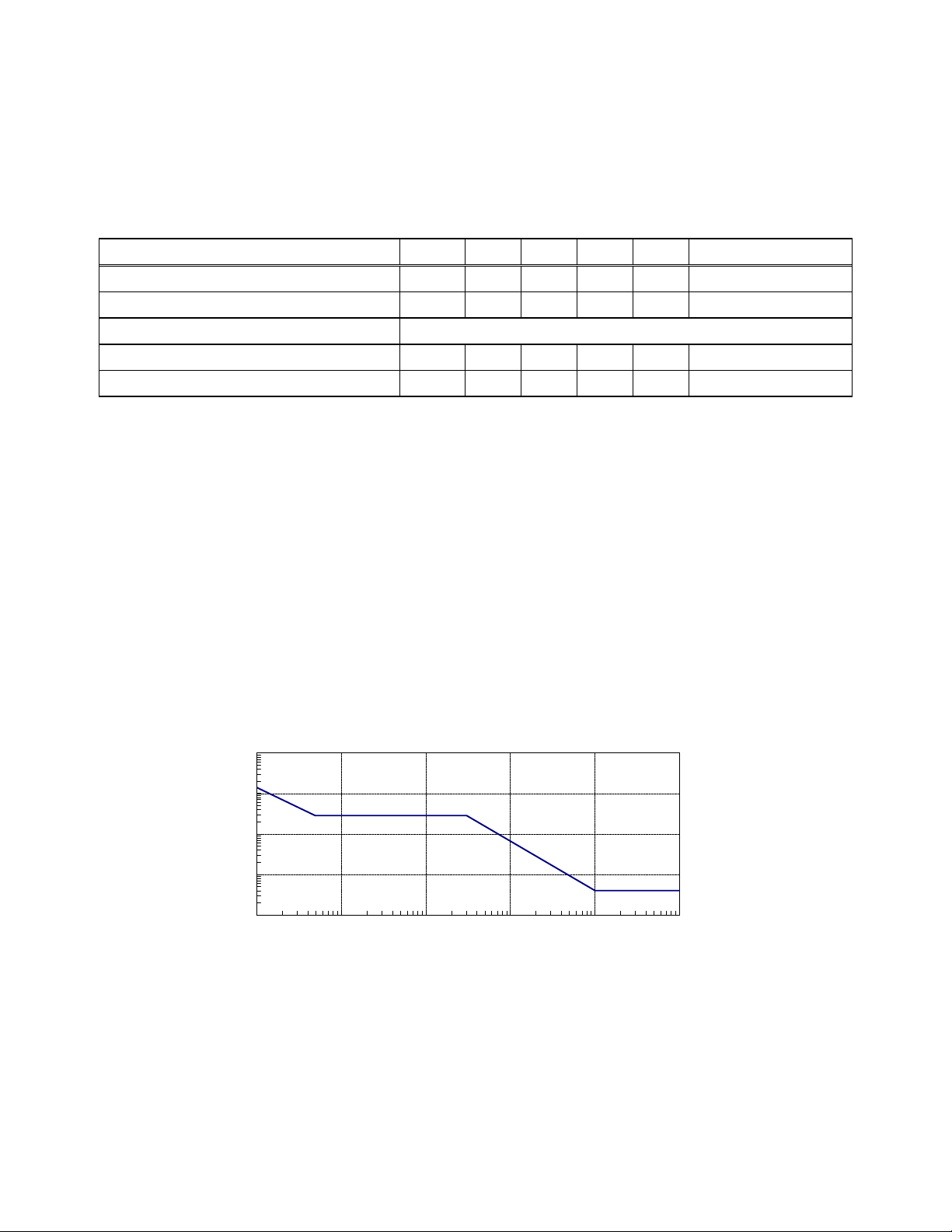
Jitter Tolerance GR-499 CategoryI,II, ATT TR 62411
Consecutive Zeros before Loss of Signal 170 175 180 Note 3
Input Impedance 20 kohm Note 4
Note 1: Relative value to the reference level. Compare at 772kHz with all mark pattern.
Note 2: Level at the line side of transformer. Loss of signal is logical OR between an analog loss of
signal, which monitors input level, and a digital loss of signal, which checks recovered data
stream.
Note 3: The device will tolerate consecutive zeros until loss of signal is reported with QRSS (PN20
Modified) pattern.
Note 4: It is not subject to be tested for the production. Guaranteed by design.
JITTER TOLERANCE
1000
100
10
1
Jitter Amplitude(UIpp)
0.1
1 10 100 1000 10000 100000
JITTER TOLERANCE
TR62411
Jiiter Frequency(Hz)
 Loading...