

AKM AK2305 Datasheet
ASAHI KASEI [AK2305]
Dual PCM CODEC for ISDN TERMINAL ADAPTER
GENERAL DESCRIPTION
AK2305 is a dual PCM CODEC-Filter most
suitable for ISDN Terminal Adapter. A-law/ulaw is selected by the internal register.
In addition to CODEC, this device has dual
DTMF receiver and External Tone Input pin.
Input/output operational amplifiers included in
this device are used for transmit/receive gain
adjustment. AK2305 has internal volume control
to attenuate signal from 0dB to –12dB by 3dB
step control which is defined by an internal
register written through the serial interface.
PCM interface of AK2305 accepts several clock
formats, which are Long Frame, Short Frame,
GCI, IDL. 64k-4096kHz clock input is available
for PCM interface.
AK2305
FEATURE
-
Dual PCM CODEC and Filtering systems for
ISDN Terminal Adapter
-
Dual DTMF Receiver
-
External Tone Input(AUX)
-
Independent functions on each channel
- Frame Sync Signal(8kHz)
- Power Down Mode(Pin/Register operation)
- Mute(Pin/Register operation)
- Gain Adjustment: 0 to -12dB (3dB step)
-
Selectable PCM Data Interface Timing:
Long Frame / Short Frame / GCI / IDL
-
Variable PCM Data Rate:
64k x N [Hz] (64k - 4.096MHz)
-
Operational Amplifier for Gain Adjustment
-
A-law/u-law Register Selectable
-
Serial Interface
-
Power on Reset
-
Single +5V ± 5% CMOS technology
-
Low Power Consumption (85mW typ)
PACKAGE
- 48LQFP
9.0 x 9.0 mm (0.5mm pin pitch)
C0029-E-02 1 1999/8

ASAHI KASEI [AK2305]
CONTENTS
ITEMS PAGE
- BLOCK DIAGRAM….…………..……………………… 3
- PIN ASSIGNMENT….……………………………..…… 4
- PIN CONDITION……...………………………………… 5
- PIN FUNCTION…….…………………………………… 6
- CIRCUIT DESCRIPTION….….……………………...… 8
- FUNCTIONAL DESCRIPTION…….…..……………… 9
- PCM INTERFACE……….…………………….... 9
LONGFRAME/SHORTFRAME……….…… 10
GCI……………………………………..…….. 12
IDL……………………………………………..13
RESET…………………………………..…… 14
- POWER DOWN……..……………………..…… 15
- MUTE…………………………………….……… 17
- GAIN ADJUSTMENT….…..…………………… 18
- DTMF RECEIVER……………………………… 19
- TONE GENERATOR…………………..………. 21
- AUX INPUT…….……………………………….. 21
- SERIAL INTERFACE………….………….…… 22
- REGISTER……….……………………………………… 25
- ABSOLUTE MAXIMUM RATINGS……..…………..…28
- RECOMMENDED OPERATING CONDITIONS…….. 28
- ELECTRICAL CHARACTERISTICS……..………...…28
- APPLICATION CIRCUIT EXAMPLE…..…………...…39
- PACKAGE INFORMATION……..…………………..… 42
C0029-E-02 2 1999/8
ASAHI KASEI [AK2305]
DTMF
Receiver0
Serial
DTMF
Receiver1
Internal
47
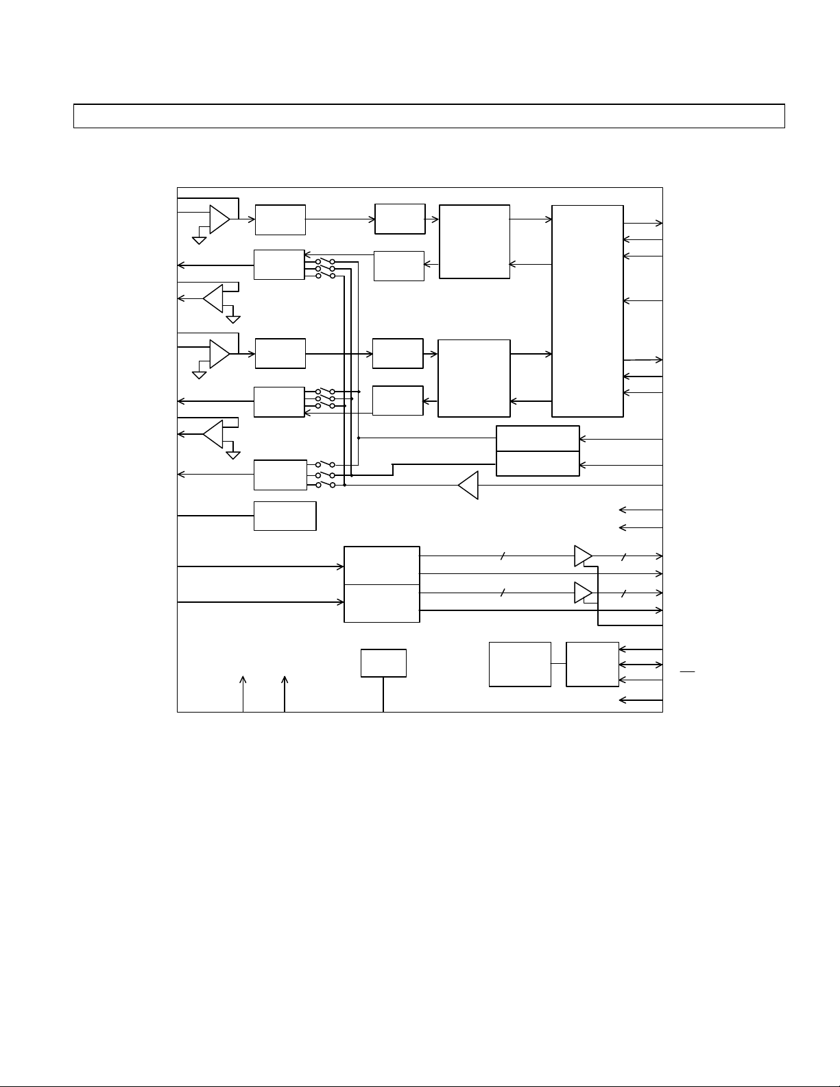
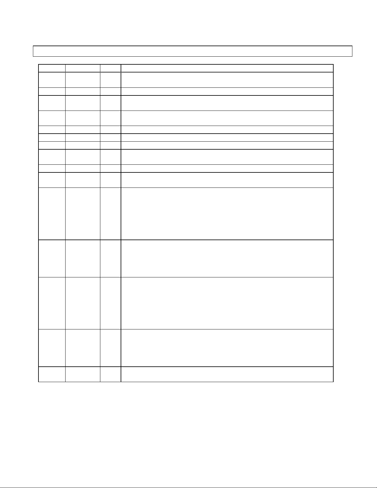
BLOCK DIAGRAM
GSX0
VFX0
VRX0
VFR0
GSR0
GSX1
VFX1
VRX1
VFR1
GSR1
TNOUT
VREF
DTIN0
DTIN1
AVDD
AVSS
DVDD
DVSS
48
1
2
3
14
13
12
11
10
9
4
46
15
6
7
31
30
VR0T
AMPT0
VR0R
AMPR0
VR1T
AMPT1
VR1R
AMPR1
VRTN
BGREF
45 16 5
TST2TST1
S1
S2
S3
S4
S5
S6
S7
S8
S9
AAF0
SMF0
AAF1
SMF1
PLL
LPC
CODEC
CH0
CODEC
CH1
TONEGEN0
TONEGEN1
4
4
Register
PCM I/F
I/F
29
DX0
33
DR0
26
FS0
27
BCLK
28
DX1
32
DR1
25
FS1
22
TNOE0
21
TNOE1
8
AUX
18
MUTE0
17
MUTE1
37-40
4
4
DTO00-03
24
STD0
41-44
DTO10-13
23
STD1
20
DTOE
35
SCLK
34
DATA
36
CS
19
PD
C0029-E-02 3 1999/8
ASAHI KASEI [AK2305]
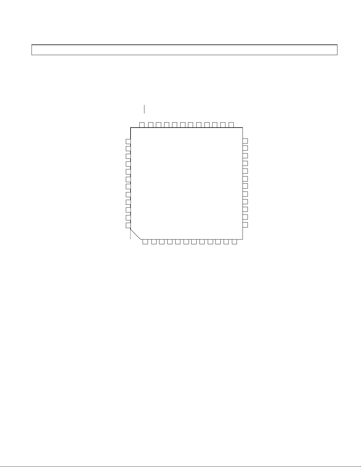
PIN ASSIGNMENT
FS1
FS0
BCLK
DX1
DX0
DVSS
DVDD
DR1
DR0
DATA
SCLK
CS
25
26
27
28
29
30
31
32
33
34
35
36
DTO00
DTO01
DTO02
DTO03
DTO10
DTO11
DTO12
DTO13
TST1
DTIN0
GSX0
VFX0
37
38
39
40
41
42
43
44
45
46
47
48
2
1
VFR0
VRX0
4
3
VREF
GSR0
5
LPC
7
6
AVSS
AVDD
9
8
TNOUT
AUX
11
10
VFR1
GSR1
24
23
22
21
20
19
18
17
16
15
14
13
12
VRX1
STD0
STD1
TNOE0
TNOE1
DTOE
PD
MUTE0
MUTE1
TST2
DTIN1
GSX1
VFX1
C0029-E-02 4 1999/8
ASAHI KASEI [AK2305]
PIN CONDITION
Pin# Name I/O Pin type
VRX0
1
VFR0
2
GSR0
3
VREF
4
LPC
5
AVDD
6
AVSS
7
AUX
8
TNOUT
9
GSR1
10
VFR1
11
VRX1
12
VFX1
13
GSX1
14
DTIN1
15
TST2 I TTL Factory use only
16
MUTE1
17
MUTE0
18
PD
19
DTOE
20
TNOE1
21
TNOE0
22
STD1
23
STD0
24
FS1
25
FS0
26
BCLK
27
DX1
28
DX0
29
DVSS
30
DVDD
31
DR1
32
DR0
33
DATA
34
SCLK
35
CSN
36
DTO00
37
DTO01
38
DTO02
39
DTO03
40
DTO10
41
DTO11
42
DTO12
43
DTO13
44
TST1 I TTL Factory use only
45
DTIN0
46
GSX0
47
VFX0
48
O Analog
I Analog
O Analog
O Analog
O Analog
-
-
I Analog
O Analog
O Analog
I Analog
O Analog
I Analog
O Analog
I Analog
I TTL
I TTL
I TTL
I TTL
I TTL
I TTL
O CMOS
O CMOS
I TTL
I TTL
I TTL
O CMOS
O CMOS
-
-
I TTL
I TTL
I/O TTL/CMOS
I TTL
I TTL
O CMOS
O CMOS
O CMOS
O CMOS
O CMOS
O CMOS
O CMOS
O CMOS
I Analog
O Analog
I Analog
AC load
(MAX.)
50pF
50pF
50pF
50pF
50pF
50pF
15pF
15pF
15pF
15pF
15pF
15pF
15pF
15pF
15pF
15pF
15pF
15pF
15pF
50pF
DC load
(MIN.)
10kΩ
10kΩ (*1)
10kΩ
10kΩ (*1)
10kΩ
10kΩ (*1)
10kΩ (*1)
Outout status
(Power down
mode)
Hi-Z Hi-Z
Hi-Z Hi-Z
Hi-Z Hi-Z
Hi-Z Hi-Z
Hi-Z Hi-Z
Hi-Z Hi-Z
L L
L L
Hi-Z Hi-Z
Hi-Z Hi-Z
Input Input
Hi-Z Hi-Z
Hi-Z Hi-Z
Hi-Z Hi-Z
Hi-Z Hi-Z
Hi-Z Hi-Z
Hi-Z Hi-Z
Hi-Z Hi-Z
Hi-Z Hi-Z
Hi-Z Hi-Z
Output status
(Reset)
Remarks
external cap
external cap
(*2)
(*3)
*1) DC load(MIN.) includes a feedback resistance of input/output op-amp. *2) Pulled down to VSS in GCI/IDL mode.
*3) Pulled down to VSS in 2ch Multiplex mode.
C0029-E-02 5 1999/8
ASAHI KASEI [AK2305]
PIN FUNCTION
Pin# Name I/O Function
VFX0 I
48
GSX0 O
47
VRX0 O
1
VFX0 I
2
GSR0 O
3
GSR1 O
10
VFR1 I
11
VRX1 O
12
GSX1 O
14
VFX1 I
13
DX0 O
29
DR0 I
33
DX1 O
28
DR1 O
32
FS0 I
26
Transmit analog input. Inverting input of transmit gain adjustment
amplifier for channel 0.
Output of transmit gain adjustment amplifier for channel 0.
Receive analog output of SMF for channel 0. This output can drive 10kΩ
and 50pF.
Transmit analog input. Inverting input of transmit gain adjustment
amplifier for channel 0.
Output of receive gain adjustment amplifier for channel 0.
Output of receive gain adjustment amplifier for channel 1.
Inverting input of receive gain adjustment amplifier for channel 1.
Receive analog output of SMF for channel 1. This output can drive 10kΩ
and 50pF.
Output of transmit gain adjustment amplifier for channel 1.
Transmit analog input. Inverting input of transmit gain adjustment
amplifier for channel 1.
Serial output of PCM data of ch0.
In Long Frame / Short Frame mode, output PCM data of ch0.
In GCI / IDL mode, output PCM data of ch0 is multiplexed with ch1. The
PCM data rate is synchronized with BCLK.
See “PCM INTERFACE” from page 9.
This output remains in the high impedance state except for the period of
transmitting PCM data.
Serial input of PCM data of ch0.
In Long Frame / Short Frame mode, input PCM data of ch0.
In GCI / IDL mode, input PCM data of ch0 is multiplexed with ch1. The
PCM data rate is synchronized with BCLK.
See “PCM INTERFACE” from page 9.
Serial output of PCM data of ch1.
In Long Frame / Short Frame mode, output PCM data of ch1.
The PCM data rate is synchronized with BCLK.
See “PCM INTERFACE” from page 9.
This output remains in the high impedance state except for the period of
transmitting PCM data.
In 2ch multiplexd mode, this pin remains in the high impedance state.
Serial input of PCM data of ch1.
In Long Frame / Short Frame mode, input PCM data of ch1. The PCM
data rate is synchronized with BCLK.
See “PCM INTERFACE” from page 9.
In GCI / IDL mode, this pin is pulled down to VSS.
Frame sync input for channel 0.
FS0 must be 8KHz clock synchronized in BCLK.
C0029-E-02 6 1999/8
ASAHI KASEI [AK2305]
CS
Pin# Name I/O Function
FS1 I
25
BCLK I
27
DTIN0 I
46
DTO00 O
37
DTO01 O
38
DTO02 O
39
DTO03 O
40
STD0 O
24
DTIN1 I
15
DTO10 O
41
DTO11 O
42
DTO12 O
43
DTO13 O
44
STD1 O
23
DTOE I
20
TNOE0 I
22
TNOE1 I
21
AUX I
8
TNOUT O
9
DATA I/O
34
SCLK I
35
36
MUTE0 I
18
MUTE1 I
17
PD I
19
LPC O
5
VREF O
4
DVDD -
31
DVSS -
30
AVDD -
6
AVSS -
7
TST1 I
45
TST2 I
16
Frame sync input for channel 1.
FS1 must be 8KHz clock synchronized in BCLK.
In GCI / IDL mode, this pin is pulled down to VSS.
Bit clock of PCM data interface. This clock is apply for both ch0 and ch1.
BCLK should be synchoronized with 8 x N kHz(FSn x N kHz).
DTMF tone input of ch 0.
Output of DTMF receiver 0. DTO00 is LSB.
Steering to delay output of ch0. After the DTMF decoding, the output
latch is renewed and this output alters to high level.
DTMF tone input.
Output of DTMF receiver 1. DTO10 is LSB.
Steering to delay output of ch0. After the DTMF decoding, the output
latch is renewed and this output alters to high level.
Output enable pin for the DTMF receiver.
Output enable pin for the tone generator 0.
Output enable pin for the tone generator 1.
External tone input pin. Input signal should be through more than 0.1uF
of an external capacitance.
Tone output pin.
Data input of serial interface.
Clock input of serial interface.
I
Read and write enable of serial interface.
Active high input for ch0 mute.
Active high input for ch0 mute.
Active high input for all power down.
Pin for PLL loop filter. Connect to AVSS with 0.22uF or larger.
Analog ground output.
To stabilize the analog ground, connect to AVSS with 0.1uF or larger.
Digital positive supply voltage. System digital +5V supply.
Digital negative supply voltage. System digital ground.
Analog positive supply voltage. Systems analog +5V supply.
Analog negative supply voltage. System analog ground.
Only for factory use. Should to be fixed to DVSS.
C0029-E-02 7 1999/8
ASAHI KASEI [AK2305]
CIRCUIT DESCRIPTION
Block Function
AMPT0,1
AMPR0,1
AAF
A/D
D/A
SMF
BGREF
TONE GEN 0
TONE GEN 1
SWITCH
Sn(n=1-9)
DTMF
Receiver0,1
VR0T/R
VR1T/R
VRTN
SERIAL I/F
PLL
PCM I/F
Op-amp for input gain adjustment. This op-amp is used as an inverting amplifier.
Adjusting the gain with external resistors. The resistor larger than 10kΩ is
recommended for the feedback resistor.
<NOTE>
AMP0(1) becomes automatically power down, when both CODEC ch0(1) and
DTMFR0(1) are power down.
Op-amp for output gain adjustment. This op-amp is used as an inverting amplifier.
Adjusting the gain with external resistors. The resistor larger than 10kΩ is
recommended for the feedback resistor.
Integrated anti-aliasing filter which prevents signals around the sampling rate
from folding back into the voice band. AAF is a 2nd order RC low-pass filter.
Converts analog signal to 8bit PCM data according to the companding schemes of
ITU recommendation G.711; A-law or u-law. The band limiting filter is also
integrated. The selection of companding schemes is set by ALAWN register as
follows:
"H": u-Law
"L": A-Law
Expands 8bit PCM data according to A-law or u-law. The selection of companding
schemes is set by ALAWN register as follows:
"H": u-Law
"L": A-Law
Extracts the inband signal from D/A output. It also corrects the sinx/x effect of
D/A output.
Provides the stable analog ground voltage (2.4V) using an on-chip band-gap
reference circuit which is temperature compensated.
Generates two kinds of tone; 400Hz and 1300Hz. Tone selection is defined by
registers. ON/OFF of tone output is controlled by TNOE0/1.
Controls output signals from VRX0, VRX1, TNOUT pins. Each switch is controlled
by register.
Detects and decodes the DTMF tone. ON/OFF of decoded output is controlled by
DTOE.
Gain selects of analog I/O signals. It is posibble to select gain from 0dB to -12dB
(3dB/step* 5steps). Gain is defined by register.
Interface to internal register by using SCLK, DATA, and CS pins.
1word=14bit; Instruction code: 2bit, address: 3bit, data: 9bit(1dummy bit
included).
PLL generates system clock of AK2305. Reference clock is FSn (8KHz). More than
0.22uF of an external capacitance should be connected between LPC and AVSS.
PCM data rate is available for 64xN(N = 1 to 64)kHz which synchronizes with
BCLK. Data format is selected in four types(Long Frame, Short Frame, GCI, IDL).
2ch PCM data are interfaced through DR0,1 and DX0,1 in non multiplexed mode
or DR0 and Dx0 in multiplexed mode.
C0029-E-02 8 1999/8

ASAHI KASEI [AK2305]
FUNCTIONAL DESCRIPTION
PCM INTERFACE
AK2305 supports the following types of format.
One of those is selected by PCMIF0 and PCMIF1 registers.
- Long Frame Sync(LF)
- Short Frame Sync(SF)
- GCI
- IDL
PCM data of both channels are multiplexed and interfaced through the common pins (DR0, DX0) in 2ch
Multiplex I/F mode. But in 2ch Independent I/F mode of LF or SF, it is also available to interface through the
independent pin(DR0/1,DX0/1) by channel.
Register of PCM interface mode selection
PCMIF1 PCMIF0 Interface Frame sync Input pin Output pin Remarks
0 0 LF/SF (Non multiplex) FS0,FS1 DR0,DR1 DX0, DX1
Reset
0 1 LF/SF (2ch multiplex) FS0,FS1 DR0 DX0
1 0 GCI (2ch multiplex) FS0 DR0 DX0
1 1 IDL (2ch multiplex) FS0 DR0 DX0
FRAME SYNC SIGNAL(Frame Sync : FS)
Frame sync signal should be 8kHz clock. 8bits PCM data is accommodated in 1 frame (125us).
Though only FS0 is required (FS1 isn’t required) in the mode of GCI or IDL, both FS0 and FS1 are required in
the mode of LF or SF.
FIRST FS
It is used as the input clock of PLL. PLL generates all timing in this IC from this signal.
FS0 is assigned as First FS in the mode of GCI or IDL, and in the mode of LF or SF, it is assigned by the first FS
register.
1stFS
register
0 FS0
First FS Remarks
Reset
1 FS1
Note
Keep supplying the first FS except for the state of all power down(PD=”H”). If the first FS is not supplied,
AK2305 loses timing; at a result, DTMFR and TONE GEN become not guaranteed to work normally.
BCLK
This clock decides the PCM data rate. See the following table of the relation between BCLK and PCM data rate.
PCM I/F mode BCLK
Rate of PCM
data
LF/SF/IDL F F
GCI 2F F
C0029-E-02 9 1999/8
ASAHI KASEI [AK2305]
Don’t
Don’t care
Don’t
Don’t care
output
output
output
output
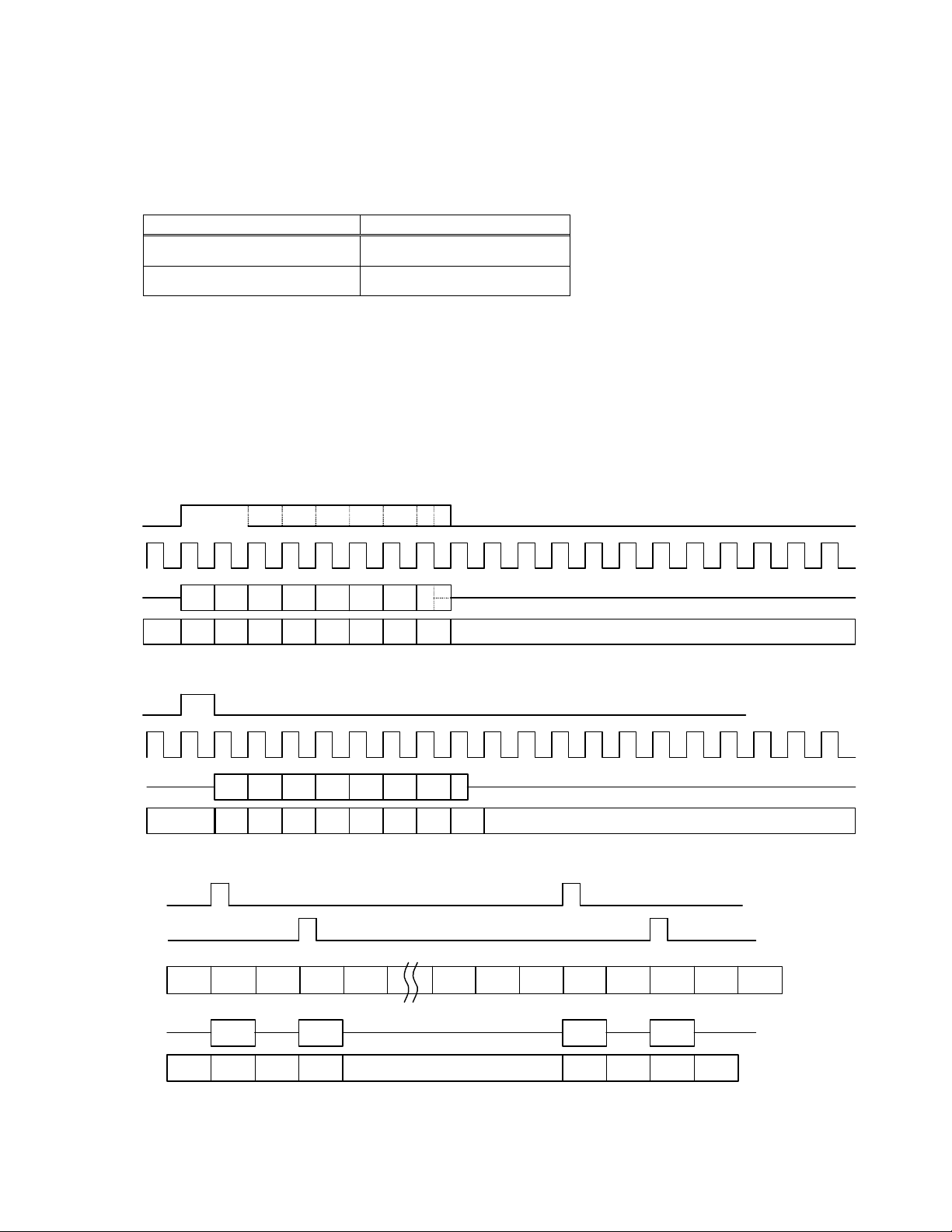
Long Frame Sync(LF) Short Frame Sync(SF)
AK2305 automatically decides whether Long Frame or Short Frame should be selected, by monitoring the high
level period of First FS.
Period of First FS =”H” Frame type
more than 2 clock of BCLK LF
1 clock of BCLK SF
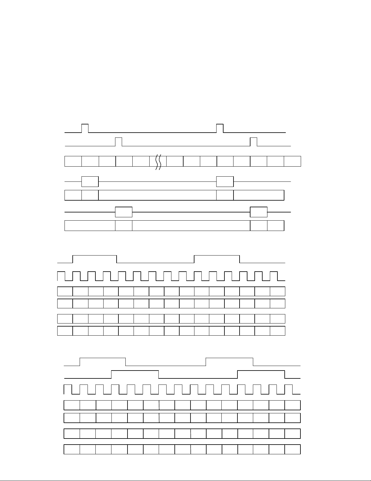
INTERFACE TIMING
<2ch Multiplex>
PCM data of both channel are interfaced by the DX0 and DR0(DX1 and DR1 are not used) at the format of
8bits in the period of 1 frame(125us) which synchronizes with the FSn(n=0,1). In the period of 1frame, 64 time
slots can be assigned at the maximum (in case of BCLK=4.096MHz). The number of the time slots is BCLK/64k.
The time slot assignment of CH0 and CH1 is decided by FS0 and FS1. In the mode of LF and SF, second FS(not
first FS) must be delayed or fast at least (8/BCLK) x n: (n=1 - 63) from the first FS.
LongFrame
FS0
BCLK
DX0
DR0
1 2 3 4
1 2 3 4 7 85 6
care
ShortFrame
FS0
BCLK
DX0
DR0
care
1 2 3 4
1 2 3 4 7 85 6
BCLK=4096kHz ( First FS = FS0 )
FS0
FS1
SLOT
1 2 3 4
5 6
5 6
7 8
7 8
63 64 1
2 3
4
DX0
DR0
ch0
ch0
input
ch1
ch1
input
ch0
ch0
input
ch1
ch1
input
C0029-E-02 10 1999/8
ASAHI KASEI [AK2305]
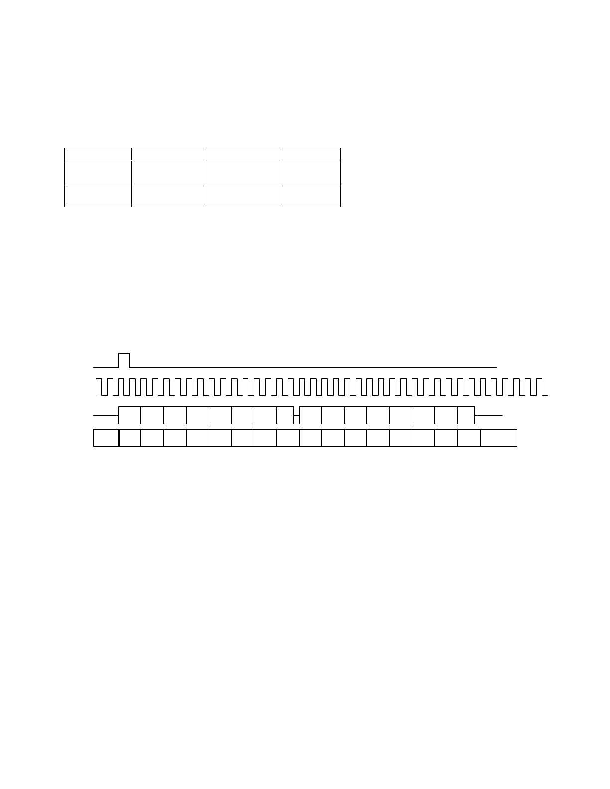
INTERFACE TIMING
<Non Multiplex>
PCM data of each channel are interfaced by each I/O pins(DX0 and DR0/DX1 and DR1) at the format of 8bits
in the period of 1 frame(125us) which synchronizes with the FSn(n=0,1). The timing of FS0 and FS1 can be set
at optionally as far as they synchronize with BCLK.
NOTE) First FS and Second FS
Only when BCLK=64kHz, it is possible to input the same clock to the first FS and the second FS. Except for
64kHz BCLK, 8 clock of BCLK x n (n=1-63 integral numbers) intervals of n slots are needed.
BCLK=4096kHz ( First FS = FS0 )
FS0
FS1
SLOT 63 64 1
DX0
DR0
DX1
DR1
1 2 3 4
ch0
output
ch0
input
ch1
output
ch1
input
ch0
output
ch0
input
BCLK=64kHz(LF) ( FS0 and FS1 at the same timing, First FS = FS0 )
FS0,FS1
BCLK
DX0
DR0
DX1
DR1
1 2 3 4
1 2 3 4
1 2 3 4
1 2 3 4
5 6
7 8 1
7 8 1 2 3 45 6
7 8 1 2 3 45 6
7 8 1 2 3 45 6
2 3 4
2 3
ch1
output
ch1
input
4
BCLK=64kHz(LF) ( First FS = FS0 )
FS0
FS1
BCLK
DX0
DR0
DX1
DR1
1 2 3 4
1 2 3 4
1 2 3 4
1 2 3 4
5 6
7 8 1
7 8 1 2 3 45 6
2 3 4
7 8 1 2 3 45 6
7 8 1 2 3 45 6
C0029-E-02 11 1999/8
ASAHI KASEI [AK2305]
Don’t
Don’t
B1-CHANNEL(CH0)
B2-CHANNEL(CH1)
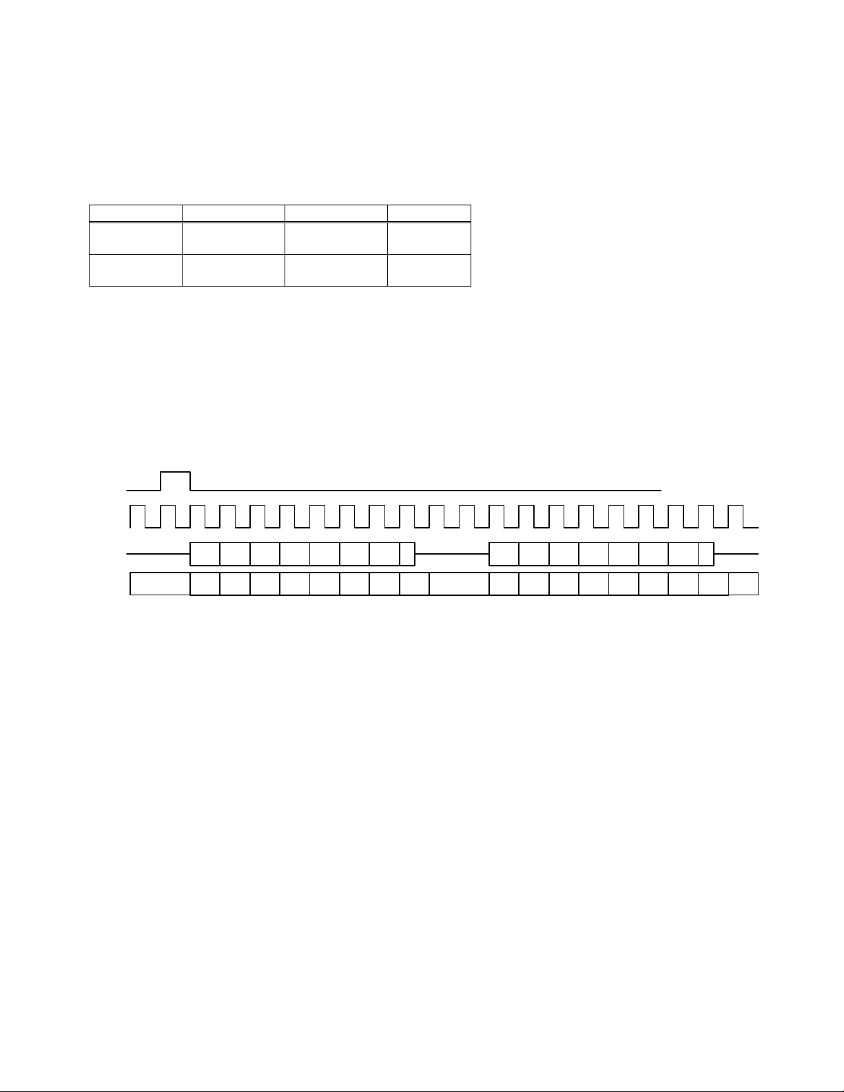
GCI(General Circuit Interface)
Interface used for ISDN. This data format is as below.
PCM data channel assignment for B1 and B2 is defined by SEL2B register.
CH0,1selection
SEL2B CH0 CH1 Remarks
0 B1 B2 Reset
1 B2 B1
Note: BCLK is twice the PCM data rate.
BCLK is acceptable from 512kHz to 4096kHz.
INTERFACE TIMING
<2ch Multiplex>
PCM data of each channel is interfaced through DR0/DX0 pin in 8bits format.
They are accommodated in 1 frame(125us) which synchronizes with FS0.
FS0
BCLK
DX0
DR0
1 2 3 4
1 2 3 4 7 85 6 1 2 3 4 7 85 6
care
<Non Multiplex>
Not supported.
5 6
<SEL2B=”0”>
7 8
1 2 3 4 7 85 6
care
<SEL2B=”0”>
C0029-E-02 12 1999/8
ASAHI KASEI [AK2305]
Don’t
Don’t
B1-CHANNEL(CH0)
Don’t
B2-CHANNEL(CH1)
IDL(Interchip Digital Link)
Interface used for ISDN. This data format is as below.
PCM data channel assignment for B1 and B2 channel is defined by SEL2B register.
CH0,1selection
SEL2B CH0 CH1 Remarks
0 B1 B2 Reset
1 B2 B1
Note: BCLK is same as the PCM data rate.
BCLK is acceptable from 256kHz to 4096kHz.
INTERFACE TIMING
<2ch Multiplex>
PCM data of each channel is interfaced through DR0/DX0 pin in 8bits format.
They are accommodated in 1 frame(125us) which synchronizes with FS0.
FS0
BCLK
DX0
DR0
care
<Non Multiplex>
Not supported.
1 2 3 4
5 6
1 2 3 4 7 85 6 1 2 3 4 7 85 6
<SEL2B=”0”>
7 8
1 2 3 4 7 85 6
care
<SEL2B=”0”>
care
C0029-E-02 13 1999/8
 Loading...