

ASAHI KASEI [AK2048]
2M
2M CMI
2M2M
CMI Transceiver
CMI CMI
AK2048D
AK2048D
AK2048DAK2048D
Transceiver
TransceiverTransceiver
- 2.048Mbps CMI Interface
- CLOCK & DATA Recovery function
- Loss of Lock Detection
- Loss of Signal Detection
- Transmitter Pulse Shape
- Single 5.0V±5% Operation
- Low Power Consumption: 400mW (TYP)
- Package: 44pin QFP
TXA
TXA
TXATXA
TXB
TXB
TXBTXB
DRIVER
RRRRXA
XA
XAXA
RRRRXXXXBBBB
VREF
RESET
FEATURES
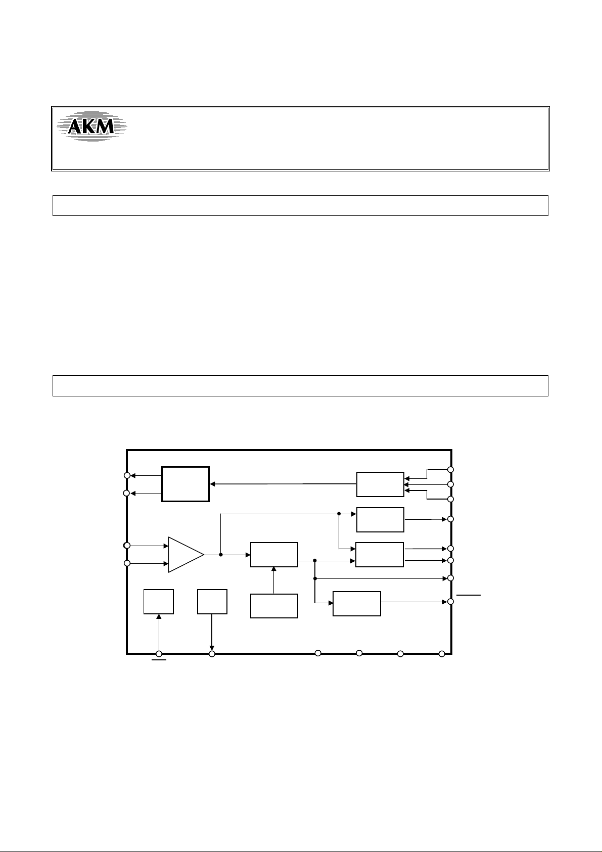
BLOCK DIAGRAM
CLOCK
RECOVER
CALIB
ENCODER
DECODER
LOCK
CMI
LOS
CMI
TDATA
TDATA
TDATATDATA
TCLK
TCLK
TCLKTCLK
TCRV
TCRV
TCRVTCRV
LOS
LOS
LOSLOS
RDATA
RDATA
RDATARDATA
RCRV
RCRV
RCRVRCRV
RCLK
RCLK
RCLKRCLK
LOCK
LOCK
LOCKLOCK
RST
RST
RSTRST
REF25
REF25 RRRRVDD
REF25REF25
2M CMI Transceiver Block Diagram
MS0073-E-00 2001/01 1
VDD RVSS
VDDVDD
RVSS TVDD
RVSSRVSS
TVDD TVSS
TVDDTVDD
TVSS
TVSSTVSS
ASAHI KASEI [AK2048]
GENERAL DESCRIPTI O NS
AK2048D is the 2.048Mbps CMI interface CMOS LSI for CMI interface card. It includes Clock and
Data Recovery, L i ne Dr i ver, LO S Det ect o r , etc.
Build in PLL clock recovery circuit eliminates the correlation of the frequency deviation due to the
uneven quality of the devices and a secular change.
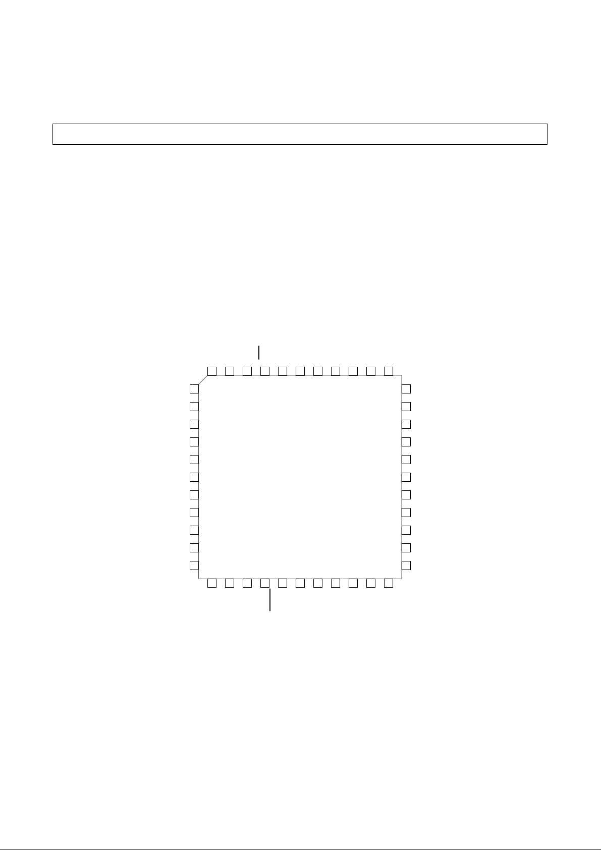
PIN ASSIGNMENTS
44pin QFP
NC
NC
NC
NC
RVDD
LOS
NC
NC
NC
NC
NC
NC
NC
NC
RXA
33
NC
32
REF25
31
NC
30
RXB
29
NC
28
NC
27
TXA
26
TVDD
25
TVSS
24
TXB
23
RDATA
RCLK
RCVR
NC
NC
NC
NC
NC
TDATA
TCLK
TCRV
NC
NC
RVSS
RST
44 43 42 41 40 39 38 37 36 35 34
1
2
3
4
5
(TOP VIEW)
(TOP VIEW)
6
(TOP VIEW)(TOP VIEW)
7
8
9
10
11
12 13 14 15 16 17 18 19 20 21 22
TEST1
TEST2
NC
LOCK
MS0073-E-00 2001/01 2
ASAHI KASEI [AK2048]
PIN ASSIGNMENTS
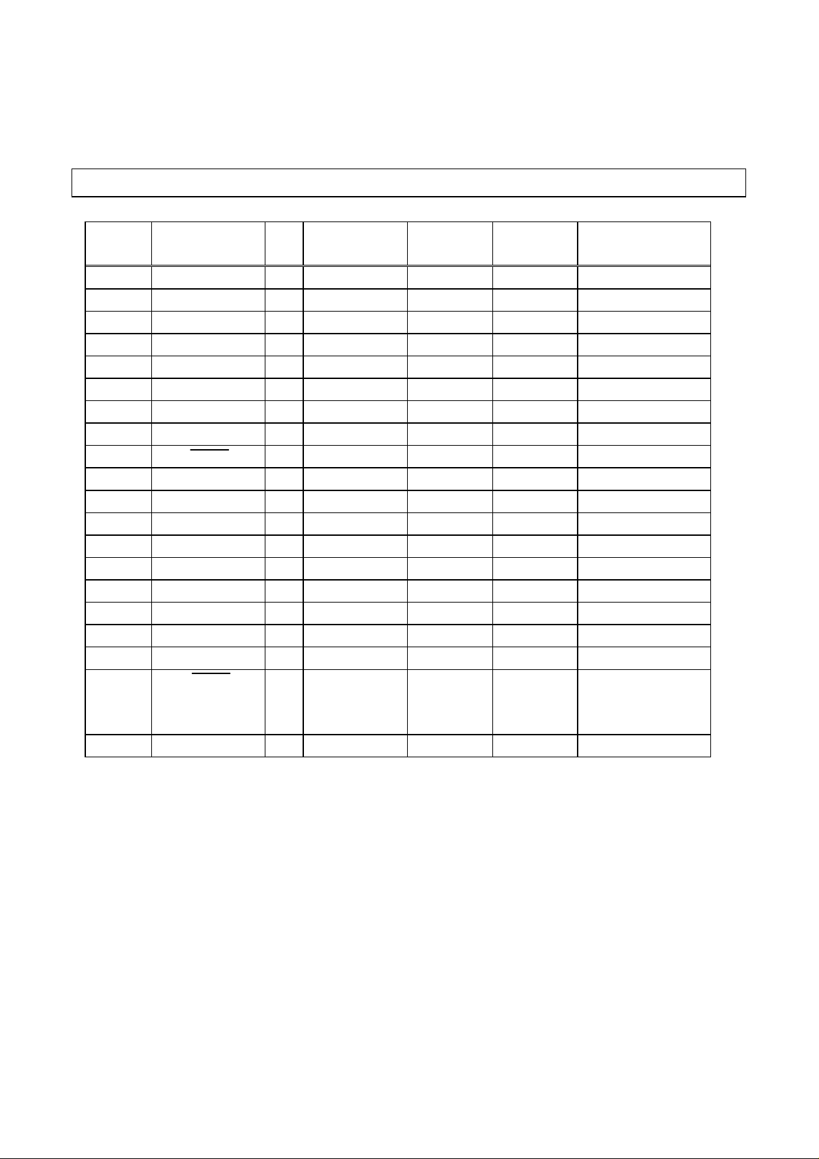
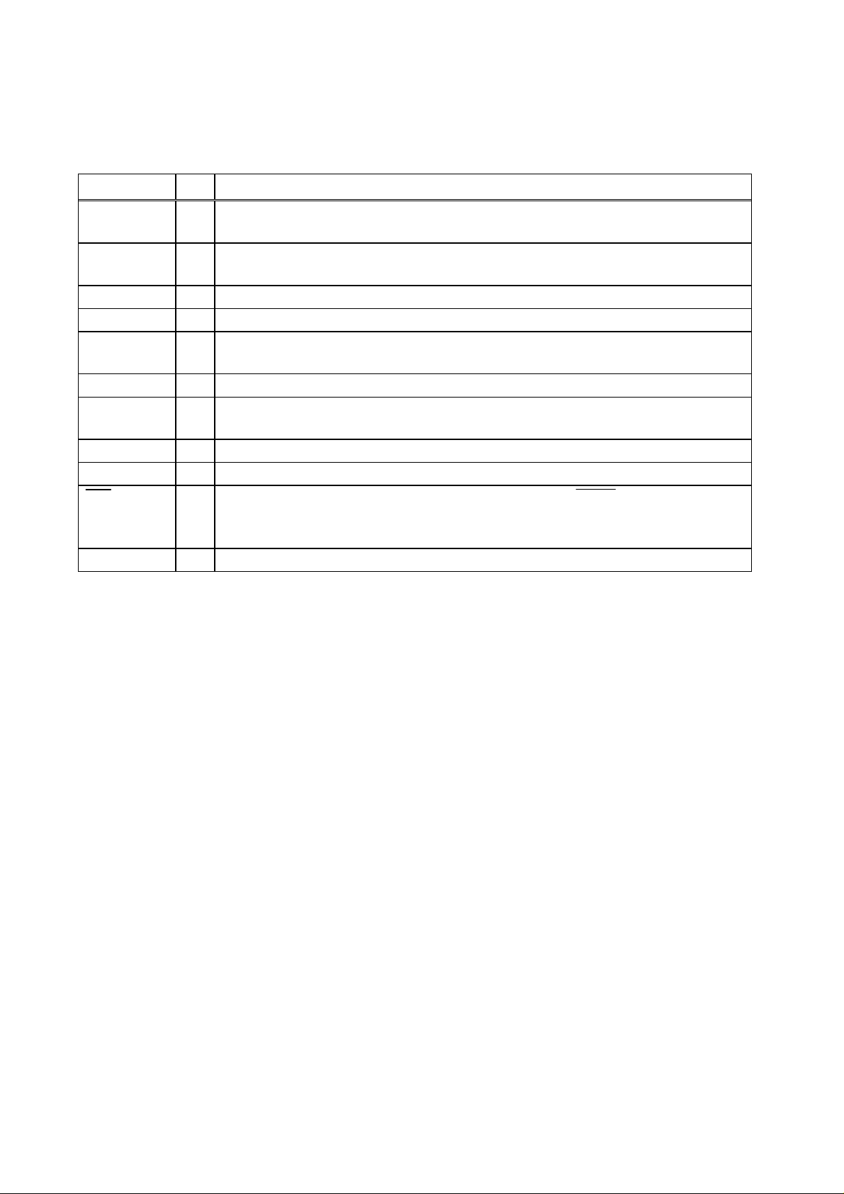
Pin No. Pin Name I/O Type AC Load
(MAX)
1
2
3
9
10
11
13
14
15
16
23
24
25
26
29
31
33
40
41
42
The other pins (4-8,12,17-22,27,28,30,32,34-39,43,44) are NC pins.
RDATA O TTL ≤15pF
RCLK O TTL ≤15pF
RCRV O TTL ≤15pF
TDATA I TTL
TCLK I TTL
TCRV I TTL
TEST1 - *2)
TEST2 - *2)
LOCK O TTL ≤15pF
LOS O TTL ≤15pF
TXB O Analog ≤15pF *1)
TVSS -
TVDD -
TXA O Analog ≤15pF *1)
RXB I Analog
REF25 O Analog 1µF(typ)
RXA I Analog
RVDD -
RST I TTL Pulled up to VDD
RVSS -
DC Load
(MIN)
≥4kΩ
≥4kΩ
≥4kΩ
≥4kΩ
≥4kΩ
Comment
by the internal
register (50KΩmin)
NC pins are recommended to connect to VSS to avoid noise problem.
*1) TXA, TXB can drive 11 0Ω connected between these pins .
*2) Must be ope n .
MS0073-E-00 2001/01 3
ASAHI KASEI [AK2048]
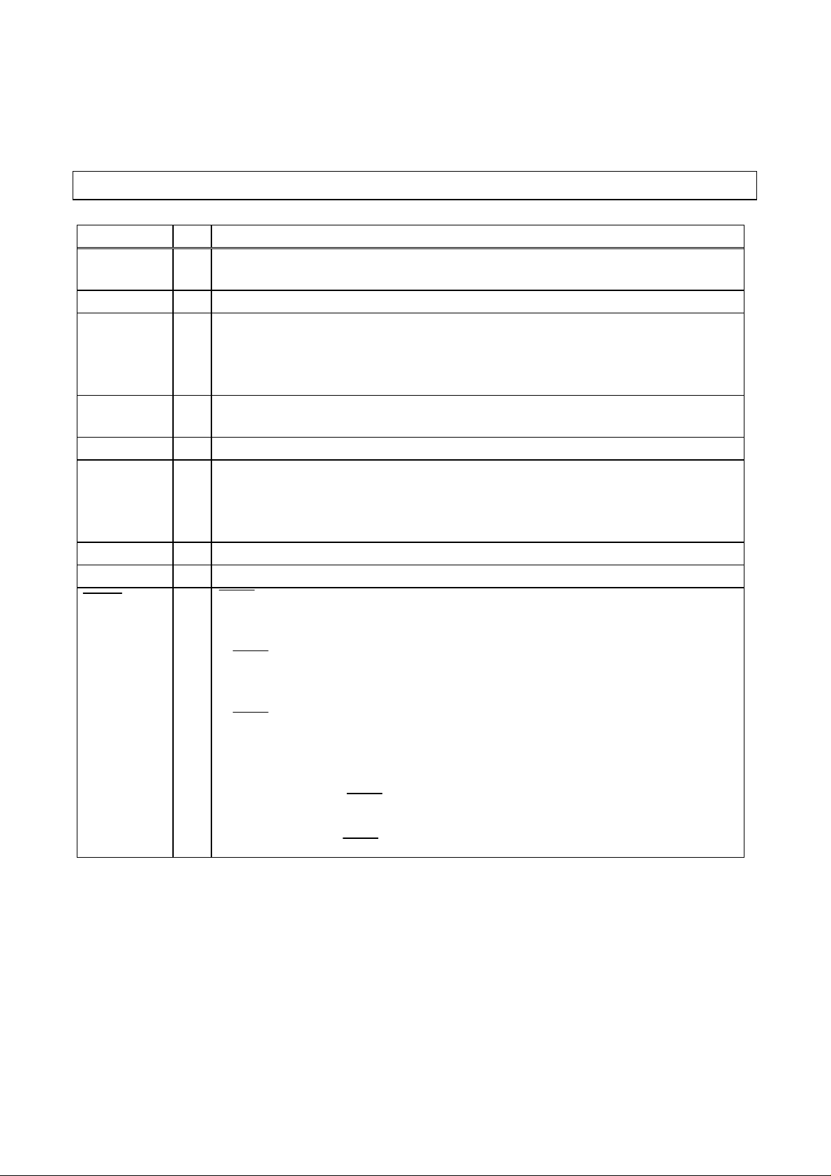
PIN DESCRIPTIONS
Pin Name I/O Function
RDATA O
RCLK O
RCRV O
TDATA I
TCLK I
TCRV I
TEST1 NC
TEST2 NC
LOCK O
Receive Data output recovered from the incoming data. Delay time from the incoming
data to the RDATA is about 1.25bit. Output on the rising edge of RCLK.
Receive Clock Output recovered from the incoming data.
CRV (Code Rule Violation) output pin .
When AK2048D detects the CRV of CMI codes from in the coming data, RCRV goes
to “high” synchronized with the violation data. CRV is detected for both “0” data and
“1” data. Refer to Fig.6, 11
Transmit Data Input pin.
Input on the falling edge of TCLK.
Transmit Clock Input pin.
If this input is “high”, AK2048D generates CR V in the transm i t d ata.
CRV is generated for both “0”data and “1”data. “High” input TCRV is accepted until 5
clocks duration. If the duration of “High” input is longer than 6 clocks, TCRV input
after 6th clock is ignored. Refer to Fig.4, 11
Test pin. Should be floated.
Test pin. Should be floated.
LOCK indicates the PLL st atus whether PLL is in the LOCK s tatus or PLL is in the
UNLOCK status.
LOCK status
LOCK becomes “Low” when the sampled RCLK are all “Low” during the consecutive
32 RXA-RXB sample clock duration.
UN LOCK status
LOCK becomes “High” when the following both conditions are satisfied.
The sampled RCLK are “High” m or e than 5 clocks in the frame of the consecutive
-
256 RXA-RXB clock duration.
And the above happens in the 5 consecutive frames.
-
In another condition, LOCK keeps the current output status without change.
The output timing of this signal is asynchronous with RCLK.
When RST is “Low”, LOCK is fixed to “High”.
MS0073-E-00 2001/01 4
ASAHI KASEI [AK2048]
Pin Name I/O
LOS O
TXB O
TVSS TVDD TXA O
RXB I
REF25 O
RXA I
RVDD RST O
RVSS -
LOS goes High within 12usec after AK2048D detects that the amplitude of the RXB
input signal is lower than 135mVpp(typ). Output on the rising edge of RCLK.
Transmit CMI signal output. TXA is to CMI+, and TXB is corresponds to CMI-.
Delay time from TDATA to TXB is about 1bit.
Negative power supply 0V
Positive power supply 5V
Transmit CMI signal output. TX A is to CMI+, and T XB is corresponds to CMI-.
Delay time from TDATA to TXA is about 1bit.
Receive CMI signal input. RXA is to CMI+, and RX B is corresponds to CMI -.
Output reference voltage (about 2.5V) in order to decide middle point of input signal
(RXA-RXB). Connected to middl e point of the external equ a l iz er.
Receive CMI signal input. RXA is to CMI+, and RX B is corresponds to CMI -.
Positive power supply .
“Low” input reset the calibration circuit and forces LOCK output “High” and
TXA-TXB output “High-Z”. When this input rise, PLL calibration restarts.
Please set open or connect to VDD when not using.
Negative power supply 0V
5V
Function
MS0073-E-00 2001/01 5
 Loading...