

Page 1

S
S
S
e
e
e
C
C
C
r
v
r
v
r
v
o
o
o
i
i
i
l
l
l
c
c
c
o
o
o
e
e
e
u
u
u
M
M
M
r
r
r
T
T
T
a
a
a
V
V
V
n
u
n
u
n
u
a
a
a
l
l
l
Page 2

2
Z
N
A
/
3
P
C
C
C
H
H
H
-
-
-
P
P
T
T
T
3
3
D
D
D
A
/
/
A
A
A
A
N
N
9
9
9
3
3
3
Z
Z
8
8
8
4
4
4
W
9
2
:
l
e
d
h
h
h
o
o
o
a
a
a
d
d
s
s
s
s
s
s
e
e
i
i
i
l
l
s
s
s
:
:
:
:
:
2
2
U
9
9
U
U
W
W
O
O
O
M
M
M
C
C
C
Model No: 29WHP3ANZ
Version 1.0
Page 3

3
CONTENT
THE MAIN CHIPS TDA9384/ TDA9363............................................................................................... 4
SIGNAL PROCESS................................................................................................................................. 7
THE HORIZONTAL AND VERTICAL CIRCUIT ................................................................................8
POWER SUPPLY .................................................................................................................................... 9
FACTORY MODE................................................................................................................................. 10
APPENDIX ............................................................................................................................................ 14
CIRCUIT DIAGRAM............................................................................................................................ 20
EXPLODED VIEW AND PART NAME.............................................................................................. 22
Model No: 29WHP3ANZ
Version 1.0
Page 4
4
THE MAIN CHIPS TDA9384/TDA9363
The UOC (“Ultimate One Chip”) TDA9363 is adopted in this chassis. This IC is the first available
component that contains the complete control and small signal functionality needed for a TV
application in one device.
1. The UOC TDA9363 pins function description: (total 64 pins
Pin1: Standby control,“1” is on,“0”is off.
Pin2: SCL.
Pin3: SDA.
Pin4: Tuning PWM output.
Pin5:
Pin6: Key board input.
Pin7: Mute control, “1” is mute, “0”is off.
Pin8: CTL, the earth magnetic field rectification output.
Pin9: Pin12, Pin18, Pin30, Pin35, Pin41, Pin55: GND.
Pin10:
Pin11: RELAY, control the K701,“1”is degaussing,“0”is not.
Pin13: SECAM PLL connected with a capacitance.
Pin14: +8V power source supply
Pin15:
Pin16: PHI-2 control loop, this pin requires a capacitor at 2.2nF (C) in series to GND.
Pin17:
Pin18: GND.
Pin19:
Pin20: East-west pillow signal output.
Pin21:
Pin22:
Pin23:
Pin24:
Pin25:
Pin26: Vertical sawtooth, This pin requires a capacitor to ground of 100nF.
Pin27: AGC output. This output is used to control (reduce) the tuner gain for strong RF signals.
Pin28: Audio de-emphasis.
Auto AV control SW, connected with the SCART2’s 8th pin.
Input. The rising edge or the falling edge operates.
LED, the lamp control output.
“1” is on standby, the lamp is light,
“0” is turn-on. The lamp is dim.
Using a capacitor of 220n in series to GND, This pin decouples the internal digital supply
voltage of the video processor and minimizes the disturbance to the sensitive analogue
parts.
PHI-1 control loop, the loop filter connected to pin 17 is suitable for various signal
conditions like strong/weak and VCR signal. This is achieved by switching of the loop
filter time constant by changing the PHI-1 output current.
Bandgap decoupling, the bandgap circuit provides a very stable and temperature
independent reference voltage. This reference voltage (4.0 V) ensures optimal
performance of the analogue video processor part of the TDA9363 and is used in almost
all functional circuit blocks.
Vertical drive output.
IF input.
Reference current, This pin requires a resistor to ground. The optimal reference current is
100mA, which is determined by this resistor. The 100mA reference current should not be
changed because the geometry processor is optimised for this current.
Furthermore the output current of vertical drive and EW are proportional to this current.
)
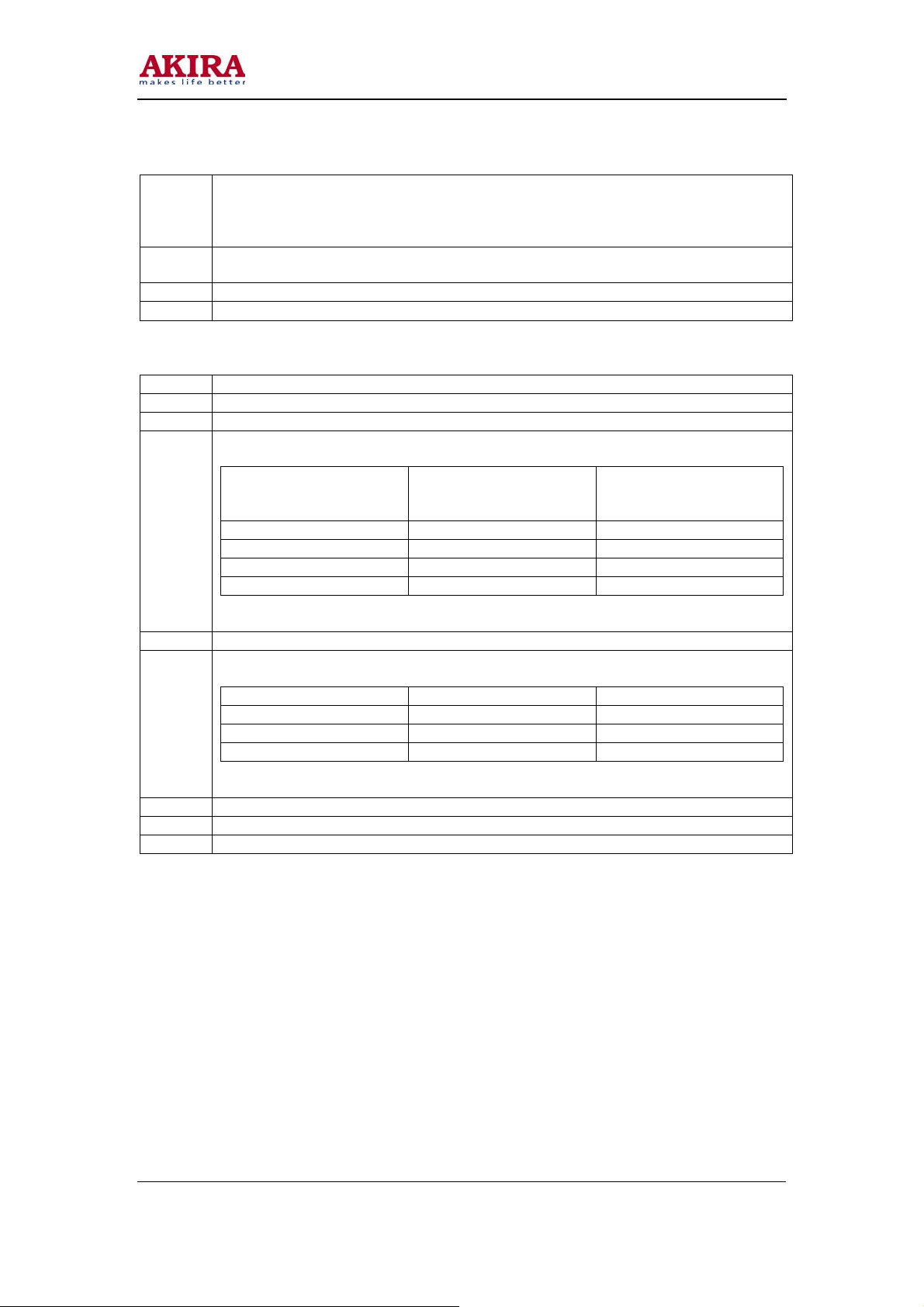
Model No: 29WHP3ANZ
Version 1.0
Page 5
5
Pin29:
Pin30: GND.
Pin31: Sound loop filter.
Pin32: AVL filter.
Pin33: Horizontal drive signal output, needs a resistor in series to +8V.
Pin34: Sandcastle output/flyback input
Pin35: External audio input, this pin should be grounded in this chassis.
Pin36:
Pin37: PLL loop filter.
Pin38: CVBS output. Monitor or RF videos can be selected.
Pin39: +8V supply source.
Pin40: CVBS input
Pin42: Y signal input.
Pin43: C signal input.
Pin44: Main audio output, this pin is connected to the TDA9859.
Pin45: RGB signal input blanking.
Pin46,
Pin47,
Pin48:
Pin49: ABL. It means been current limiter input. The R410 is the control resister.
Pin50: Black current input from the CRT board.
Pin51,
Pin52,
Pin53:
Pin54: +3.3V.
Pin55: GND.
Pin56: +3.3V.
Pin57,
Pin58,
Pin59:
Pin60: Reset, NC in this chassis.
Pin61: +3.3V
Pin62: NC.
Pin63: This pin is connected to the HEF4094, Functions expanding.
Pin64: IR signal input.
Sound decoupling. This pin requires a capacitor connected to ground. The pin acts as a
low pass filter needed for the DC feedback loop.
EHT tracking/ overvoltage protection. If something is wrong, the anode high voltage rises,
the heater voltage will rise too. When the rising voltage arrive some limit, the V406
works, the voltage of pin 36 will exceed 3.9V, the TDA9363 will stop working.
RGB signal input.
RGB drive signal output to the CRT board.
12MHz crystal.
Model No: 29WHP3ANZ
Version 1.0
Page 6
6
2. Memory AT24C08 is an E
Pin1,
Pin2,
Pin4,
Pin7:
Pin3,
Pin8:
Pin5: SDA.
Pin6: SCL.
GND.
+5V-1 supply.
2
PROM of 8k, pins describe as follows:
3. HEF4094B is described as follows:
Pin1: Connected with UOC Pin63.
Pin2: SDA.
Pin3: SCL.
AV control switch output, connected to the HEF4052. Data as follows:
HEF4094B Pin5
HEF4052 Pin9
Pin4,
Pin5:
Pin8: GND.
Tuner bands control output. Data as follows:
HEF4094B Pin11 HEF4094B Pin 12 Band
Pin11,
Pin12:
Pin14: NC.
Pin15: Control port, it is high level in this chassis.
Pin16: +5V supply.
0 0 AV1
1 0 AV2
0 1 AV3
1 1 SVHS
0 0 VHF-L
1 0 VHF-H
0 1 UHF
total 16 pins)
(
HEF4094B Pin4
HEF4052 Pin10
STATE
Model No: 29WHP3ANZ
Version 1.0
Page 7

7
SIGNAL PROCESS
The main chip is N201 TDA9363, AV control switch HEF4052, sound process chip is TDA9859,
sound driver is N601 TDA7495S.
The TV signal inputs into the tuner (U101) from CABLE or antenna. The pin 11 and pin 12 of the
N502 are combined to select the band. The pin 4 of the N201 outputs the PWM tuning signal. The IF
video signal comes from the IF pin of the tuner. The 38.9MHz IF signal is coupled to the N101 (preamplify) and then to SAWF (Z101). After processed in the SAWF, the 38.9MHz signal gets to the pin
23 and pin 24 of TDA9363. The IF circuit in TDA9363 includes such unit as the AGC amplifying
circuit, 38.9MHz oscillator, PLL video demodulator, video amplifier, IF identify circuit and AFT
circuit. The demodulated signal (CVBS) comes from the pin 38 of TDA9363, the sound signal comes
from the pin 44.
The internal CVBS signal needs norm identification then outputs from the pin 38 of TDA9363, via the
trap-wave circuit (composed of the V504, Z501, Z502, Z503, V506 and so on) feeds back to the pin 40
of TDA9363. The RGB signal comes from the pin51, Pin52, Pin53 of TDA9363, and outputs to the
CRT board.
The V901, V902 and V903 are the R
V909 are the auto low bright balance level output circuit, and generate the low bright level current into
the pin 50 of TDA9363.
The internal sound signal comes from the pin 44 of TDA9363, via the coupling capacitor C224
connects to the pin 3 and 5 of TDA9859. The TDA9859 is the audio effect processor, the TDA9495S is
the driver. The TDA9859 includes bass, treble, balance, surround, effect shortcut options.
G B drive transistors. The V904, V905, V906, V907, V908,
、、
Model No: 29WHP3ANZ
Version 1.0
Page 8

8
THE HORIZONTAL AND VERTICAL CIRCUIT
Through Synchronous separating circuit, the video signal is divided into horizontal-Synchronizing
signal and Vertical-Synchronizing signal. The horizontal-Sync pulse coming from the pin 33 is
transferred to the horizontal-drive transistor, and will be used to drive the horizontal-transformer. The
horizontal-switch transistor is V405, it and the +B supply drives the flyback transformer to generate
the anode high voltage, the focus voltage, the screen voltage, the CRT board drive voltage 190V, the
vertical drive voltage 17V and 54V.
The East-west pillow signal comes from the pin 20 of TDA9363. The wave is amplified to modulate
the horizontal drive circuit. The amplifying circuit composed of the V401, V403, V402 and other
peripheral parts.
The vertical sawtooth wave is generated on the pin 21 and 22, and then enters the vertical output
amplifier circuit. The vertical output amplifier circuit is realized with the power amplifier IC –
TDA8351.
The TDA8351 is a 9 pins vertical deflection circuit (3 Amperes) for DC-coupled 90° or 110°deflection
systems with frame frequencies from 50 up to 120 Hz. Only a single supply voltage for the scan and a
second supply for the flyback are needed.
The vertical drive currents of TDA9363 pins 21 and 22 are connected to input pins 1 and 2 of the
TDA8351. The currents are converted into a voltage by resistor R305. Pin 2 is on a fixed DC level
(internal bias voltage, about 2.3V) and on pin 1 the drive voltage can be measured (typical 1.4 Vpp).
The outputs (pins 4 and 7) are connected to the series connection of the vertical deflection coil and
feedback resistor R306 and R308. The voltage across R306 and R308 is fed via pin 9 to obtain a
deflection current which is proportional to the drive voltage. The supply voltage for the TDA8351 is
17V at pin 3. The flyback generator has a separate supply voltage of 54V on pin 6. On pin 8 a vertical
guard signal is available. For HF loop stability a damping resistor R309 is connected across the
deflection coil.
Model No: 29WHP3ANZ
Version 1.0
Page 9

9
N
N
N
N
N
N
POWER SUPPLY
The IC of KA5Q1265RF is adapted in this chassis; it is the product of Fairchild. It supplies four DC
voltages, one is the +B
fourth is +16V. The +16V can generate the +8V, +5V and +3.3V by the special generators.
Fig.2 The power supplies illustration.
130V, another is Hcc 25V, the third is 27V (the sound drive voltage), the
==
L701
L703
VD705
VD706
VD707
VD708
+190V To CRT board
+17V To Pin 3 of N301
+54V To Pin 6 of N301
+8V To N101, N201, N1001/2/3, CRT board
+3.3V To N201
To N202, N502, NA01
C811
801
T801
802
+5V
803
VD812
VD813
VD811
VD810
VD401
VD402
VD403
VD830
+5V-1
+25V To V712, T402, V404
+27V To N601
+16V To V711
+12V
T401
804
805
703
Model No: 29WHP3ANZ
Version 1.0
Page 10

10
FACTORY MODE
SC-1033 UOC factory menu 1 Value Description
PARA5/6 (50H/60H) 31 Parallelogram
BOW5/6 (50H/60H) 31 Bow
HPS5/6 (50H/60H) 31 Horizontal center
WID5/6 (50H/60H) 31 Width
DPC5/6 (50H/60H) 31 Parabola
UCNR5/6 (50H/60H) 31 Up-corner
LCNR5/6 (50H/60H) 31 Low-corner
KEY5/6 (50H/60H) 31 Trapezium
SC-1033 UOC factory menu 2 Value Description
VLIN5/6 (50H/60H) 31 Vertical linearity
HIT5/6 (50H/60H) 31 Vertical amplitude
VSC5/6 (50H/60H) 31 Vertical S-correction
VP50/60 (50H/60H) 31 Vertical center
OSDV5/6 (50H/60H) 31 OSD vertical position
VX 30 Vertical amplify
RCUT 31
GCUT 31
SC-1033 UOC factory menu 3 Value Description
RDRV 31
GDRV 31
BDRV 31
WBBRI 31
WBCON 60
LANG 4 OK language option
YDFP 7 Y-delay: SECAM/PAL/NTSC individually
AGC 28
M
#
#
#
#
#
#
#
#
M
#
#
#
#
#
L
#
#
M
#
#
#
L
L
L
L
L
Model No: 29WHP3ANZ
Version 1.0
Page 11

11
SC-1033 UOC factory menu 4 Value Description
VOL 20 TDA9859 volume
9874 10 TDA9874AH volume
IFFS 2 IF option
HDOL 8 Cathode inspect level
AGCS 1 AGC operate speed
VG2B 39 Screen adjust state
TILT 31
VX16 2 Vertical amplify in 16:9 state
SC-1033 UOC factory menu 5 Value Description
OSDL 0 OSD bright
BCF 2 Start time in M state
OKBCF 4 Start time in OK state
BRI50/60 (50H/60H) 39 Sub-bright
CON50/60 (50H/60H) 61 Sub-contrast
COL50/60 (50H/60H) 61 Sub-color
SHA50/60 (50H/60H) 31 Sub-sharpness
HUE50/60 (50H/60H) 50 Sub-tint
SC-1033 UOC factory menu 6 Value Description M
M
#
L
L
L
L
L
#
#
M
L
L
L
#
#
#
#
#
OPT1 204 Refer to Table 3
OPT2 3 Refer to Table 3
OPT3 115 Refer to Table 3
OPT4 243 Refer to Table 3
OPT5 55 Refer to Table 3
OPT6 127 Refer to Table 3
INIT Reset
M legend explain:
# : Manufacture adjusting item
L : Soft relative items
M state entrance process:
quickly step by step press the key mute, call and 980.
L
L
L
L
L
L
L
Model No: 29WHP3ANZ
Version 1.0
Page 12

12
Option of menu 6
OP_DEFAULT_OPT_1 0x098 /*
OP_DEFAULT_OPT_2 0x003 /*
OP_DEFAULT_OPT_3 0x0F3 /*
OP_DEFAULT_OPT_4 0x0FB /*
OP_DEFAULT_OPT_5 0x03F /*
VG2 mode No
Comb filter No
Super woofer No
AV3 Yes
SVHS Yes
DVD No
RGB No
OSO Yes */
AVL Yes
Auto Sound Yes
National Option table 1 No
National Option table 2 No
National Option table 2 No
Function 1 No
Function 2 No
FSL No */
AFC_SAVING Yes
NV_8598 Yes
CHARGING No
SECAM_SVM No
Sound DK Yes
Sound BG Yes
Sound I Yes
Sound M Yes */
FMWS Yes
Direct switch on Yes
AKB No
LOGO Yes
HCO Yes
IDENT_SENSITIVE Yes
STABLE Yes
DFL Yes */
TILT Yes
NICAM Yes
BOX Yes
MONITOR Yes
CALENDAR Yes
GAME Yes
RESERVED No
ZOOM 16:9 OSVE No */
Model No: 29WHP3ANZ
Version 1.0
Page 13

13
OP_DEFAULT_OPT_6 0x07F /*
OP_DEFAULT_OPT_7 0x00D /*
OP_DEFAULT_OPT_8 0x004 /*
ENGLISH YES
SPANISH YES
ARABRIC YES
GERMAN YES
FRENCH YES
ROMANIAN YES
TURKISH YES
RUSSIAN NO */
OP_FARSI YES
OP_MALAYSIA No
OP_ITALIAN YES
OP_HUNGARY YES
OP_MAGNETIC
OP_HOTEL NO
OP_AGCL1 NO
OP_AGCL2 NO */
OP_BBSW NO
OP_BLACK_BACK NO
OP_CURTAIN YES
Model No: 29WHP3ANZ
Version 1.0
Page 14

14
APPENDIX
HEF4052B illustration
Model No: 29WHP3ANZ
Version 1.0
Page 15

15
TDA9859 illustration 1
Model No: 29WHP3ANZ
Version 1.0
Page 16

16
TDA9859 illustration 2
Model No: 29WHP3ANZ
Version 1.0
Page 17

17
TDA8351 illustration 1
Model No: 29WHP3ANZ
Version 1.0
Page 18

18
TDA8351 illustration 2
SYMBOL PIN DESCRIPTION
|
1 Input power-stage (positive);
drive (pos)
Includes |
|
Vp 3 Operating supply voltage
V
GND 5 Ground
VFB 6 Input flyback supply voltage
V
V
V
2 Input power-stage (negative);
drive (neg)
Includes |
4 Output voltage B
O(B)
7 Output voltage A
O(A)
8 Guard output voltage
O(guard)
9 Input feedback voltage
|(fb)
signal bias
(sb)
signal bias
(sb)
Model No: 29WHP3ANZ
Version 1.0
Page 19

19
KA5Q1265RF illustration
Model No: 29WHP3ANZ
Version 1.0
Page 20

20
CIRCUIT DIAGRAM
TUNNER
C102
47uF 16V
1
A1
A0
AU
YCVBS2
LIN
RIN
TO A2 XS507TO A2 XS506
7
XP502
(EMC) U101
AGC1VT2AS3BS14BS25VCC6+5V
100u 16V
C105
C104
C103
100u
100u
+5V
L101
100u 16V
10uH
C107
C101
C108
100u 16V
10n
+
R101
R102
100K
+33V
IF
8
7
9
10
R217
R216
12K
10K
C206
100n
22k
HEF4 094
N502
1
STR
VDD
2
SDA
E0
3
SYSTEM
SCL
4
MUTE
00
5
BAND2
01
6
BAND1
02
7
03
8
Vss
R151
11
33
R150
100
16
15
14
13
12
11
10
9
uPC574
VD201
R214
R215
12K
C240
10n
10K
C205
100n
V201
PH2369
+5V -1
R525
10
R580
5k6
R526
3k3
+5V
R527
3K3
R528
3K3
R103
680
+8V
1
CIN
VOUT
SDA
SCL
10
XP503
XP810
14
+24V
GND
+130V
GND
TO A5 XP603
C513
1n
C514
47n
R521
XP804
1
3
VD803
EU2A
R806
2
56k
(EMC)N801
KA5Q1265RF
47u/50V
DRAIN1GND2Vin3OCP/F.B4SOURCE
C818
330uF/220V
R818
56k
L805
C801
2n2
C813
TRG1C
470
VD802
VD808
EU2A
C803
100n/50v
680p/1KV
R812
10
VD804
EU2A
R811
470
VD805
3V1
R807
56k
C814
39n/50V
22n/400V
C811
2
5
VD897
1N4148
R810
(EMC)T801
3
3
7
1
2
C810
2n2/400V
4
C802
N802
HS817B
14
12
9
13
15
10
16
11
8M2R814
1
23
C833
100n/50V
+8V
47
(EMC)VD810
RU4AM
(EMC)VD812
R836
1k
R835
1k
C109
12k
R213
C204
10u
C507
C822
470p/500V
(EMC)VD813
RU4Z
C825
10n
47u
N101
IN1GND2Vp
3
+130V
2
Z102
39.5M
A1015
C585
33n
R584
R583
10k
10k
R115
82K
R227
4k7
1
WP
2
n.c.
3
A2
4
Vss
24C08N202
R524
220
L820 L821
C838
220u/160V
470p/1kV
(EMC)VD811
BYD33D
L806
C823
470p/500V
L807
R828
RU4Z
C824
C834
220u/25V
L801
R831
470p/500V
1R2
KA431LZ
VD820
1N4148
V805
VD820
R438
C1815
4k7
R837
100k
OUT
4
5
6
10
C112
R122
R120
4K7
10n
R121
3K3
V518
VD101
BAT81
R111
2K2
V517
A1015
Vdd
PTC
SCL
SDA
20kR523
V509
C1815
2
R829
22k
22u/250V
R823
2R2
+16V
1
R840
5k1
+26V
R839
10k
RP801
50k
10
V102
C1815Y
R116
56K
+5V -1
R226
100
8
R225
7
3k3
6
5
C201
C203
56p
10n
C508
R522
47u
470
+130V
C828
+12V
R834
220k
L7808CV
R841
C831
5k1
220u/25V
+8V
L201
10uH
C261
C260
100u 16V
4
5
+8V
C835
100u
N803
BA33T
In Out
N805
L7805CV
In Out
Gnd
R201
3K3
VD830
1N4148
+5V
Gnd
C837
100u
+3.3V+5V -1
10n
(EMC) Z101
K628 3D
1
2
8
3
R224
3k3
C202
56p
+24V
C826
220u/35V
R820
L808
39
2
N804
In Out
Gnd
L810 L809
+5V -1 +5V
+5V -1
C832
TO A4 XS707
XP201
1
LED
100R208
100R209
C201
56p
R206
+3V3
3k3
C210
C211
16V
100n
100u
C407
1uF
16V
100u
10
+12V
CTL
IR
RELAY
STAN DBY
KEY
R201a
5k6
R212
R202
5k6
5k6
TDA9 38XN201
1
Standby
56pC202
2
SCL
3
SDA
4
Tuning
5
R207
SVHS
47
6
Key
7
MUTE
8
CTL
R203
9
R255
100
15KR410
16V
2u2C215
R219
16V
C222
R223
3k9
R506
1K8
R507
1K8
V505
C1815
R520
10K
Vss C/ P
100
10
LED
11
RELAY
12
VssA
C207
13
SECPLL
220n
14
Vp2
15
DECDI G
220nC208
16
PH2LF
2n2C209
17
PH1LF
4n7C2 09
18
Gnd3
100nC214
19
DECB G
20
AVL/E WD
100
21
VDRB
22
VDRA
23
IF1
24
IF2
39kR222
25
IREF
C216
26
VSC
100n
27
Tuner AGC
C217
28
AUDEE M/SIF 1
3n3
29
DECS DEM/SIF 2
10u
30
C220
Gnd2
330
31
SNDPLL/SIFAGC
32
AVL/RE FO
C221
1n2
V525S
C1815
1k
R248S
R260S
1k
L501
C1815
V504
R508
R509
56
Z502
180
XT-6.0
L502
XT-5.5
6.8uH
R510
100
R511
180
XS725
R517
Z504
56
XT-4.5
1
5
6.8uH
XT-6.5
Z501
Z503
R223S
1k8
V526S
C1815
R512
56
INPSEL
XTALout
XTALin
OscGn d
Blan king
BCLin
B2/Uin
G2/Y in
R2/Vin
INSSW2
AUDOUT/ AMOUT
CHROMA
CVBS/Y
CVBSINT
IFVO/ SVO
PLLIF
EHTO
AUDEX T/QSS O
FBISO
27n
C246
R513
1K8
R514
330
R518
1K
R519
V508
1K
C1815
VddP
Reset
VddC
VddA
Gout
Gnd1
H. out
V507
C1815
IRin
STR
VpE
Bout
Rout
Vp1
V506
C1815
+8V
+8V
R515
20
C235
2u2 16V
C236
R516
C238
330n
R505
47
C506
47u
16V
100
(EMC)Z201
12MHz
390R2 32
1k8
R230
22p C233
10uHL203
R261S
100
100nC223
R243
R242
22nC230
22nC228
47u/50V
+12V
100n
L205
10uH
C234
22p
100
100
100R241
10KR240
C417
R422
100
R611
3k3
C611
2u2
16V
64
63
62
61
60
59
58
57
56
55
54
53
52
51
50
49
48
47
46
45
44
43
42
41
40
39
38
37
36
35
34
33
TO A4 XP725
Note: This circuit diagram covers a basic or representative chassis only. There may be some component or partial circuit differences between the actual chassis and the circuit diagram.
Model No: 29WHP3ANZ
Version 1.0
TO A5 XP901 TO A2 XS509
61 14
XP202
ROUT
GOUT
BOUT
+3.3V
L204
10uH
C232
16V
100u
VD202
8V2
C231
100n
VD203
8V2
22nC229
+8V
R262S
V527S
1K
C1815
R263S
220
C225
22n
R231
27k
T402
C418
47 0p/5 00V
R423
2k2
C415
VD602
1N4148
A1015
390p
1SS133VD601
330u/25V
C610
R601
100k
V604
R602
220k
C609
R603
1n
2k7
R655
10k
V404
C2383
TO A5 XP601
BLANK
+8V
R245
33k
R244
22k
VD210
VD204
8V2
R2361KR2371KR238
1K
L202
10uH
C226
100u
BCT-5E
VD604
1SS133
V606
C1815
R607
10k
8V2
R424
C227
82
VD603
1SS133
12
R239
1K
R247
1n
R608
33k
XP205
YUV
+15V
C303
R301
2
2n2
R304
2R2
2k2
+45V
R220
100
C304
R303
2n2
2k2
R221
100
C218
1n
C219
1n
3k
+8V
R235
100k
R234
22k
9n1/2KV
9n1/2kV
C420
C421
L480
V405
D2553
C422
33n/630V
+26V
C603
22n
C602
2200u/35V
C612
470u
16V
C607
10u
16V
C424
BY228
VD412
VD413
BYV95C
N601
TDA7495S
Ri1VS2Wo3GND4Li5Wi6SVR7GND8MUTEw9MUTE10GND11Lo12Vd13Ro14GND
C607
2u2
16V 16V
R604
2k7
C407
330u/25V
15n
220u/25V
R302
VD406
15V
VD404
8V2
+15V
+24V
C606
2u2
C301
33
R428
47k
V401
C1815
R305
470K
R407
100K
R426
6k8
1N4148
C608
1n
TDA8 351N301
I+1I-2Vp3VOB4Gnd5VFB6VOA7Vguard8VIFB
C302
C307
47u/100V
100n
100n
C308
VD302
BVA21
VD301
UZ15 BSB
R414
VD405
1N4148
1k
R415
680
220p/500V
C416
R420
4k7
VD401
BYV95C
VD402
+45V
BYD33C
VD403
BYD33C
C409
4u7/250V
4u7/100V
68kR427
C423
R430
12kR425
6R8
R429
2k7
270p/500V
V403
A1015
V402
VD411
C3852
C660
10u
16V
R652
10k
C601
10u
16V
R654
6k8
47n/100V
R412
2R2
C306
C414
R310
12K
R308
2R2
R306
2R7
R403
2R2
R404
2R2
R405
2R2
C406
470p/500V
R406
220K
9
1K5
R311
+130V
L403
600uH
C415
330n/400V
R418
100
2
15
R307
2K7
10
2
1
6
8
5
4
3
9
JC30L401
R417
1k
(EMC)T401
C413
1u/160V
L404
XS401
4
R416
200k
1
11
12
13
R408
10k
7
VD409
1N4148
C663
10 00u/ 35V
2
R309
270
2
C662
1000u/35V
XP401
XP402
TO A5 XP902TO A3 XS605TO A3 XS606
HI VOL
FOCUSE
SCREEN
R409
1k
VD407
1N4148
C410
10u/25V
C305
22n
XP601
4
R SP
L SP
1
XP603
6
SDA
SCL
RIN
LIN
1
9
LIN
RIN
+5V
+8V
WIN
1
XP604
L302
L301
HEATER
+200V
R410
+8V
4k7
C412
68n
L402
6.8mH
Page 21

21
A2
Y
U
R552
V
R551
150
R541
150
V1
L1
R1
V2
150R544
L2
R2
VO
LO
RO
VHS
A3
6
ROUT
LOUT
1
XS605
SDA
SCL
9
LIN
RIN
+8V
TO A1 XP604 TO A1 XP603
1
XS606
Note: This circuit diagram covers a basic or representative chassis only. There may be some component or partial circuit differences between the actual chassis and the circuit diagram.
TO A1 XP205
411 5
XS509
YUV RL V
150
R542
47k
R543
47k
R545
47k
R546
47k
1n
C567
1n
C569
R550
R549
150
150
100u 16V
R628
1k8
C619
R616
10n
10
C640
10u/16V
1k8
R630
TO A 7 XP11 01
XP11 01
N503
HEF4053
1
C521
10u/ 16V
10kR530
C627
15n
C626
15n
C624
C633
10u/16V
33n
10u/ 16V
C579
C623
C576
5n6
R620
2
3
4
5
6
7
10u/1 6V
N504
1
2
3
4
5
6
7
C523
10k
C577
10u/1 6V
C560
C517
R568
C559
10k
1n
R570
C563
1n
R571
10k
R569
10k
10k
C568
1n
C570
1n
N602
SCIN
P1
MAIN
CSMO
MINR
VP
SC-R
GND
MoR
LR
CBR1
CBR2
CTR
LoR15LoL
SCL16SDA
C562
1n
C564
1n
C566
1n
TDA9859
SCIN
AUX
CPS1
MAD
CPS2
MAD
CBL1
CBL2
C519
10u/1 6V
P2
SC-L
MoL
LL
CTL
10u/1 6V
10u/1 6V
C520
C518
10u/1 6V
470u/16V
C524
32
31
30
29
28
27
26
25
24
23
22
21
20
19
18
17
1n
C561
1n
C565
1n
10kR572
R573
10k
220
R548
220R547
1
2
470nC615
3
C616
4
5
470nC617
6
7
C618
100u 16V
8
9
10
11
C620
33n
12
13
C622
5n6
14
100
R618
100
R619
Y1
Y0
Z1
Z
Z0
INH
VEE
VSS8C
HEF4052
0Y
2Y
Y-C
3Y
1Y
INH
VEE
VSS8B
22R531
10u/1 6V
16
VCC
15
Y
14
X
13
X1
12
0X
R577
11
A
10
B
VD561
1N414 8
9
16
VCC
15
2X
14
1X
10uC5 25
13
X-C
C518
12
0X
10u
11
3X
10
A
9
10kR529
R574
C529
10
10n
100u/16V
C528
1
A1
A0
XS1101
L
TO A 2 XP11 01TO A4 XP720
AUo
YC
GND
Lin
Rin
TO A1 XP50 2
XP502
7
1
+8V
Cin
GND
SW
Vo
SDA
SCL
GND
TO A1 XP50 3
10
XP503
V
L
V
R
XPK05
CK01
10n
TO A4 XP72 2
R540
C522
3k3
10u/1 6V
VD560
1N414 8
C530
10n
C575
R533
220k
R538
3k3
10u/1 6V
R575
C526
100u/16V
V511
2SC18 15
R532
1k
10
R537
10
A8
A6
TV/A V
R536
220k
CA01
4u7/16V
VDA01
SK06
RK01
2k2
SK05
MENU
V510
2SC18 15
R535
1k
47u/ 16V
NA01
RA02
330
XSA01
RK02
1k5
C527
SK04
VOL-
C574
100n
RK03
SK03
VOL+
47u/1 6V
C578
A7
R
XP1101
RK05
RK04
470
680
820
SK01
SK02
CH+
CH-
3k3
A5
TO A1 XP202
TO A1 XP40 2
R925
6
1
4
XP902
1
22
8V
R
G
B
HEATER
+190V
GND
R927
R926
22k
47u/16V
C909
GND
2k2
V910
2SA1015
VD910
1N4148
R929
10k
C910
R903
22u/250V
ROTATE
L706
L704
C902
R923
10
C907
390
R906
10k
C730
4u7/35V
V712
R767
2SB892
270
R762
5k1
V711
2SB892
R797
100k
R764
3k3
RT701
PTH451C7R0021
(EMC)L703
R701
2M2
1N4148VD908
15k
R930
R920
18k
C908
1n
VD907
1N4148
V704
C1815
2
10u/16V
C770
VD721
1N4148
VD720
1N4148
C701
220n/AC250V
47R901
V703
A1015
R705
1R
R717
3
3
VD906
BAV21
R922
470
V909
BF422
V908
BF423
R909
470
3DA4544
1N4148
4k7
1RR706
(EMC)L701
V901
R913
470
VD902
C726
10n
V705
C1815
C724
10u/25V
K701
(EMC)VD705-708
V710
C1815
R719
47k
VD903
1N4148
C723
100n
RM11C
10k
R931
R708
R761
R902
15k
39
47u/35V
5k1
C727
R912
10
C906
R713
VD909
1N4148
470u/16V
C912
C911
47u/16V
3DA4544
R903
100uH
V903
10k
R924
470
VD904
1N4148
1k
R907
C901
220n/500V
12n
47
R905
47
L901
A4
+5V
C729
10n
R763
10k
5
+25V
+13V
3
+16V
R766
TO A1 XS72 5
1
6R8
XP725
R765
10k
XP705
1
3
XP704
XP701
F701
T4A/AC250V
R930
15k
V902
3DA4544
R916
470
390
2
39
VD713
1N4148
R914
18k
C904
1n
R915
10
C905
390
R911
18k
C903
1n
N703
L7805CV
C728
1n
V702
C1815
C702
100n/AC250V
R918
R910
470
R760
5k1
2u2/16V
470
R919
470
R908
470
V905
BF423
+5V -1
R718
68k
C725
(EMC)C714-717
V904
BF422
R714
10k
2n2/1kV
V907
BF422
V906
BF423
VD901
BAV21
R715
1k
R750
4k7
C781
100n
VD905
BAV21
XS901
R917
C705
470p
XP903
XP903
C704
470p
XP722
+5V -1
STANDBY
RELAY
C913
2n2/2kV
XP720
LED
KEY
CTL
+16V
+5V
XS707
VE901
HI VOL
FOCUSE
FOCUSE
TO A6 XPK0 5
IR
TO A1 XP201 TO A8 XSA01
1kR936
1kR921
1k
R728
100
R726
10k
Model No: 29WHP3ANZ
Version 1.0
Page 22

EXPLODED VIEW AND PART NAME
22
Model No: 29WHP3ANZ
Version 1.0
Page 23

 Loading...