

Page 1

S
S
S
e
e
e
C
C
C
r
v
r
v
r
v
o
o
o
i
i
i
l
l
l
c
c
c
o
o
o
e
e
e
u
u
u
M
M
r
T
r
r
M
T
T
a
a
a
V
V
V
n
u
n
n
u
u
a
a
a
l
l
l
Page 2

2
E
C
/
3
S
H
T
4
1
:
l
e
d
M
o
o
o
d
d
e
e
l
l
:
:
1
1
4
4
T
T
H
H
S
S
3
3
/
/
C
C
E
E
M
M
C
C
C
h
h
a
a
s
s
s
s
i
i
s
s
:
:
U
U
O
O
O
U
:
s
i
s
s
a
h
C
C
C
-
-
-
O
O
O
M
M
M
8
8
8
3
3
3
7
7
7
0
0
0
Model No: 14THS3/CE.doc
Version 1.0
Page 3

3
CONTENT
SAFETY NOTICE.......................................................................................................................................4
GENERAL DESCRIPTION........................................................................................................................6
TECHNICAL SPECIFICATION................................................................................................................7
GENERAL SPECIFICATION....................................................................................................................8
HORIZONTAL AND VERTICAL CIRCUIT............................................................................................9
CHASSIS BLOCK DIAGRAM ................................................................................................................10
FAULT FINDING TREES........................................................................................................................11
IC BLOCK DIAGRAM.............................................................................................................................18
FACTORY MENU
EXPLODED VIEW AND PART NAME.................................................................................................43
BOM LIST .................................................................................................................................................44
CIRCUIT DIAGRAM ...............................................................................................................................64
....................................................................................................................................40
Model No: 14THS3/CE.doc
Version 1.0
Page 4

4
SAFETY NOTICE
WARNING: BEFORE EXAMINING AND
SERVICING THIS CHASSIS, READ
CAREFULLY THE FOLLOWING
SAFETY INSTRUCTIONS.
X-RAY RADIATION PRECAUTION
1. The primary source of X-RADIATION in television receiver is the picture tube. The picture tube
is specially constructed to limit X-RADIATION emissions. For continued X-RADIATION
protection, the replacement tube must be the same type as the original including suffix letter.
Excessive high voltage may produce potentially hazardous X-RADIATION. To avoid such
hazards, the high voltage must be maintained within specified limit. Refer to this service manual,
high voltage adjustment for specific high voltage limit. If high voltage exceeds specified limits,
take necessary corrective action. Carefully follow the instructions for +B1 volt power supply
adjustment, and high voltage check to maintain the high voltage within the specified limits.
2. The EHT must be checked every time the receiver is serviced to ensure that the CRT does not emit
X-ray radiation as result of excessive EHT voltage. The nominal EHT for this receiver is 22KV at
zero beam current (minimum brightness) operating at AC 220V. The maximum EHT voltage
permissible in any operating circumstances must not exceed 25KV. When checking the EHT, use
the High Voltage Check procedure in this manual using an accurate EHT voltmeter.
3. The only source of X-RAY radiation in this receiver is the CRT. To prevent X-ray radiation, you
should use the same type of CRT when replacing it.
4. Some components used in this receiver have safety-related characteristics preventing the CRT
from emitting X-ray radiation. For continued safety, replacement component should only be made
after referring the Product Safety notice below.
SAFETY PRECAUTION
1. The high voltage in the TV reaches to 22KV when the TV is in operation. Be more careful during
opening the back cover.
a) The high voltage existing in the TV is very dangerous. Refer servicing to qualified personnel
only.
b) Before removing the high voltage cap. Discharge the anode of the CRT and the chassis in
case of electric shock.
c) Wear a pair of goggles when handling the CRT to avoid broken pieces damaging your eyes.
d) Do not hold the CRT neck in case of causing damage to the CRT.
2. When the power cord needs replacing, use the same one as that provided by AKIRA factory.
3. Voltage exists between the hot and cold ground when TV is in operation. Install a separation
transformer during repairing or connecting to any tester for the sake of safety. The power of the
separation transformer should be beyond rated overall power.
4. When replacing a burnout fuse, use the one with the same specifications as the original.
Model No: 14THS3/CE.doc
Version 1.0
Page 5

5
5. When replacing old wire, wind new one round the shaft to weld. When replacing components with
safety in performance, use the same type as that specified by AKIRA and install it in the former
way.
6. Never place wire near high-temperature or high-voltage components.
7. An isolation transformer should be connected in the power line between the receiver and the AC
line when a service is performed on the primary of the converter transformer of the set.
8. Comply with all caution and safety-related notes provided on the cabinet back, inside the cabinet,
on the chassis or the picture tube.
9. When replacing a chassis in the cabinet, always be certain that all the protective devices are
installed properly, such as, control knobs, adjustment covers or shields, barriers, isolation resistor-
capacitor networks etc.. Before returning any television to the customer, the service technician
must be sure that it is completely safe to operate without danger of electrical shock.
PRODUCT SAFETY NOTICE
Product safety should be considered when a component replacement is made in any area of a receiver.
Components indicated by mark in the parts list and the schematic diagram designate components in
which safety can be of special significance. It is particularly recommended that only parts designated
on the parts list in this manual be used for component replacement designated by mark. No deviations
from resistance wattage or voltage ratings may be made for replacement items designated by mark.
Model No: 14THS3/CE.doc
Version 1.0
Page 6
6
GENERAL DESCRIPTION
THE SURVEY
Table 1, the main IC and functions
Number Function IC Remark
1 Power supply KA5Q0765RT N611
2 CPU + SIGNAL PROCESSER OM 8370 /TDA9370 N301
3 Field driver STV9302A N401
4 Sound driver AN7522N N161
5 AV SWITCH TC4052BP
6 Memory AT24C08 N702
7 Photo-coupler PC817B N504
8 IR-receiver HS0038A2 U701
9 8V regulator L7808CV N503
10 5V regulator L7805CV N505
SIGNAL PROCESS
N801 (Video)
N161 (sound)
The TV signal enters into tuner (A201) from cable or antenna. Pin 10 and pin 11 of N301 are combined
to select the band. Pin 4 of N301 outputs PWM tuning signal. The 38.9MHz IF signal is coupled to
V308 (pre-amplify) and then to SAWF (Z301). After processed in the SAWF, the 38.9MHz signal gets
to pin 23 and pin 24 of OM8370. The IF circuit in OM8370 includes such unit as the AGC amplifying
circuit, 38.9MHz oscillator, PLL video demodulator, video amplifier, IF identify circuit and AFT
circuit. The demodulated signal (CVBS) comes from the pin 38 of OM8370, the sound signal comes
from the pin 44.
The internal CVBS signal needs norm identification then outputs from pin 38 of OM8370, via the trap
circuit (composed of the V351, Z351, Z354, V352 and so on) feeds back to the pin 40 of OM8370. The
RGB signal comes from pin51, Pin52, Pin53 of OM8370, and outputs to the CRT board. The internal
sound signal comes from pin 44 of OM8370 and then input to pin 1 and pin 12 of HEF4052BP. The
sound signals from RF and AV are selected in it. The selected signal is output from Pin 3 and pin13,
then input AN7522N (sound amplifier) or output from AV terminals.
Model No: 14THS3/CE.doc
Version 1.0
Page 7
7
TECHNICAL SPECIFICATION
Test Item Conditional TD171
AC Operating
Range
Total Power
Consumption
EHT
Anode Current Brightness &contrast Maximum I
Heater Voltage TV operate normally V
B+ Normal operating VB+ = 112Vdc
Sound power
output
RF&AV signal input with sound loud speaker
(volume maximum) & Picture set in Dynamic
mode
Philips or Mono-scope pattern signal with howling
sound Contrast & Brightness set in Maximum,
sound increase maximum
Standby Mode 14 Watts
Brightness & contrast set in Maximum Min: 26.2KVdc
Typical Design value Average: 26.5KVdc
Brightness &contrast Minimum Max: 27.8KVdc
RF signal input broadcasting at
217.25MHz/BG/DK(1KHz)
Volume is maximum
140Vac ~ 240Vac
90Watts
≤ 1.2mA
ABL
= 6.2Vac
Heater
V = 6.3Vrms
P = 5Watts X 2
Model No: 14THS3/CE.doc
Version 1.0
Page 8
8
GENERAL SPECIFICATION
Power consumption
Receive system DK/BG/I
Color system PAL/ SECAM/ NTSC
Vision intermediate frequency 38.9MHz
Inter-carrier frequency
Chroma if frequency PAL 34.47/ 35.32MHz
Antenna type DIN TYPE 75 Ohm
Channel receiving
Tuning system VS tuning
AV IN/ OUT 2 AV STEREO IN + 1 AV STEREO OUT
Component IN 1 YUV-Component IN
AV IN/ OUT specification
OSD language
Audio output power > 8W (1KHz, 0.5V INPUT, 10% THD
Safety authentication standard CB
LED indicator Power ON
Hand set type HS08
Hans set power supply Pin AAx2
Color picture tube 14” 21” 90 degree tube
Remote control distance 5m
External input/output
2
I
C Bus Control
Auto Search
Off/On Timer
Teletext
Model No: 14THS3/CE.doc
Version 1.0
14” 70W MAX
21” 90W MAX
5.5 MHz(B/G)
6.5MHz(D/K)
VHF Low channel (VL) =48.25
VHF high channel (VH) =154.25
UHF channel (U) =471.25
VIDEO IN ----1.0 0.2V
AUDIO IN ----0-2V (RMS)
VIDEO OUT ----1.0 0.2V
AUDIO OUT ---- 0-2V (RMS)
English, Russian, Turkish, French, Spanish,
Vietnamese, Indonesian, Arabian, Persian
Video/Audio (L/R) 2set input
YUV input
S-Video input
Video/ Audio (L/R) 1 set output
75 Ohm
p-p
p-p
to
147.25
MHz
to
463.25
MHz
to
863.25
MHz
75 Ohm
Page 9

9
HORIZONTAL AND VERTICAL CIRCUIT
Through Synchronous separating circuit, the video signal is divided into horizontal-Synchronizing
signal and Vertical-Synchronizing signal. The horizontal-Sync pulse coming from pin 33 is transferred
to the horizontal-drive transistor.
The cathode driving voltage 180V vertical drive voltage +15V and –15V are all generated from
FBT.
The vertical sawtooth waveform is generated on the pin 21 and 22, and then enters the vertical
amplifier STV9302A. STV9302A is a 7 pins vertical deflection circuit (2 Amperes) for DC-coupled
90° or 110° deflection systems with frame frequencies from 50 up to 120 Hz. one supply voltage for
the scanning and second voltage supply for the flyback are needed.
The vertical drive currents of OM8370 pins 21 and 22 are connected to input pins 1 and 7 of
STV9302A. The vertical scanning output is coming from pin 5 and feed back to pin 1 by R405. The
supply voltage is ±15V at pin 2 and pin 4. C406 is the pump capacitor.
POWER SUPPLY
The IC of KA5Q0765RT is adapted in this chassis; it is the product of Fairchild. It supplies four DC
voltages, one is the +B=110V, another is Hcc=26V, the third is 13V (the sound drive voltage), the
fourth is +16V. The +16V can generate the +8V, +5V and +3.3V by the special generators.
Model No: 14THS3/CE.doc
Version 1.0
Page 10
10
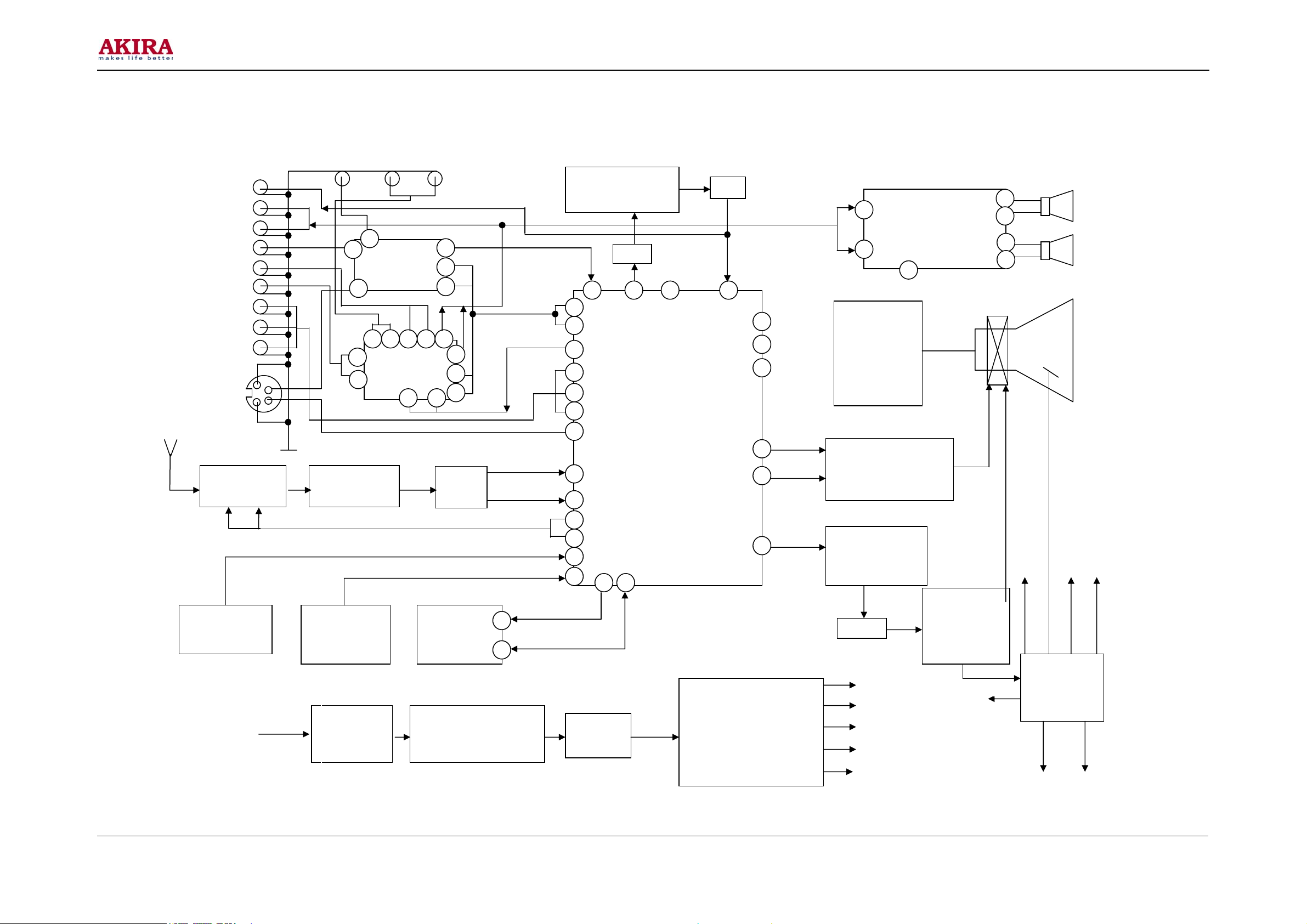
6
3
CHASSIS BLOCK DIAGRAM
Video-out
Audio-out L
Audio-out R
Video-in1
Audio-in1L
Audio-in1R
Y
Cr
Cb
S-video
HF TUNER
A101
BAND1
BAND2
KEY BOARD
AC150-260V
50/60Hz
V-in2 A-in2LA-in2R
14
15
N801CD4052
11
11
15
IF PRE-AMP
V308
REMOTE
RECEIVER
U701
AV SWITH
14
AV SWITH
N161CD4052
12
13
9
10
2 3 4 5
13
10
1
SAWF
Z301
MEMORY
N702
ST24C08
Resistance
disturbance
C501L502
rectification
VD503-VD506
TV AUDIO OUT
9
Bridge
SIF TRAPS
Z351,Z352,Z354
V352
6
AUDIO AMPLIFIER
12
10
SP161
8Ω5W
R
(N101) AN7522N
SP162
L
8Ω5W
63
62
44
47
46
48
43
V351
42
38 7
PHILIPS UOC
TDA9351/61/81
40
53
52
51
21
8
9
VIDEO
AMPLIFIER
V912V913
V922V923
V932V933
FIELD OUTPUT
4
2
CRT
POWER AMP
23
24
11
10
22
33
N401LA78040
HORIZONTAL
DRIVE
V450
64
2
SCL
6
SDA
5
T450
HORIZONTAL
OUTPUT
V451
EHT
SCREEN
HEAT
FOCUS
FBT(T402)
BSC25
-15V
Filter C507
+300V
POWER SUPPLY
CIRCUIT
V1512V553V1511T
501N504
16V
13V
15V
24V
110V
200V
+15V
Model No: 14THS3/CE.doc
Version 1.0
Page 11
11
N
N
N
N
N
N
N
N
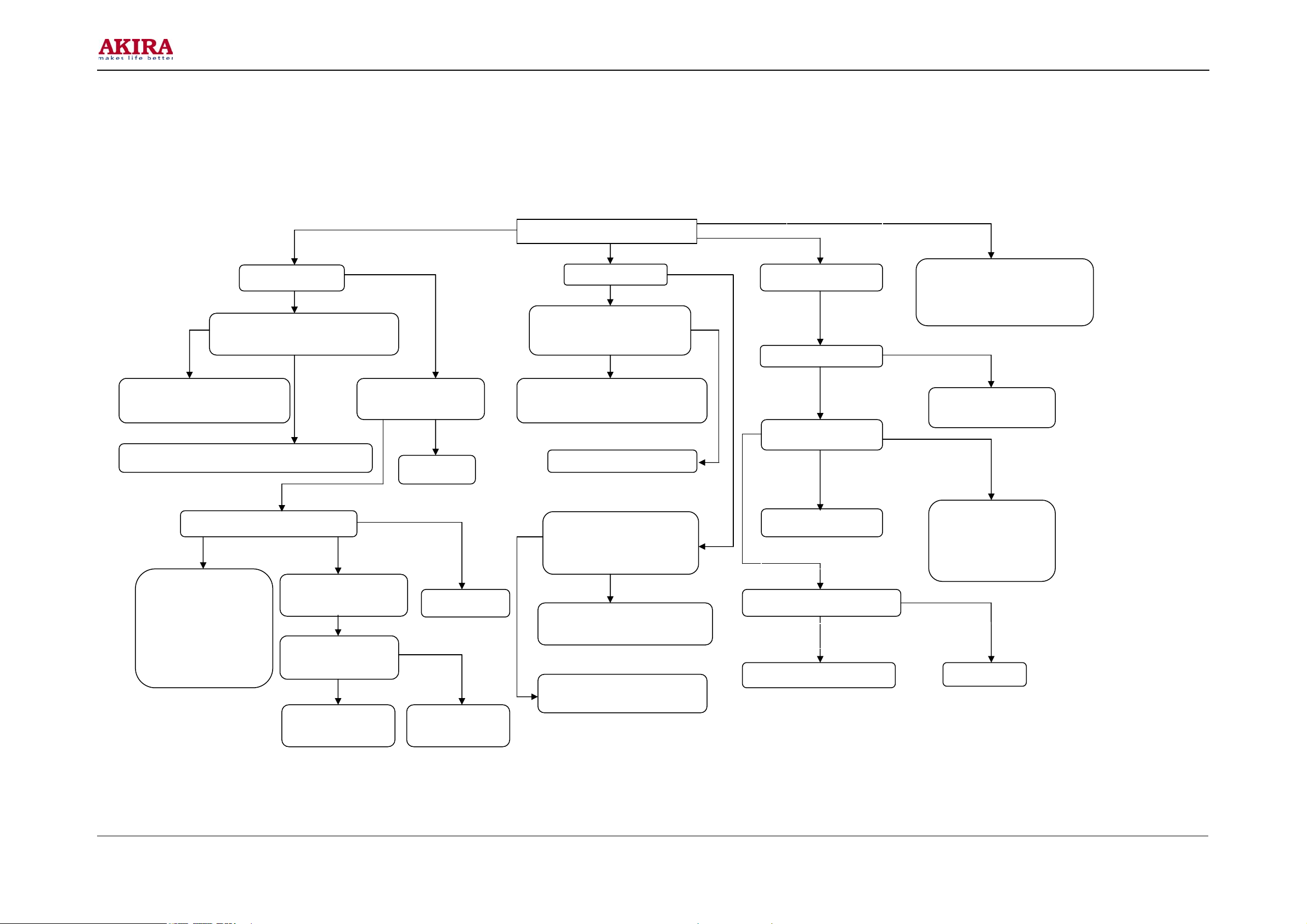
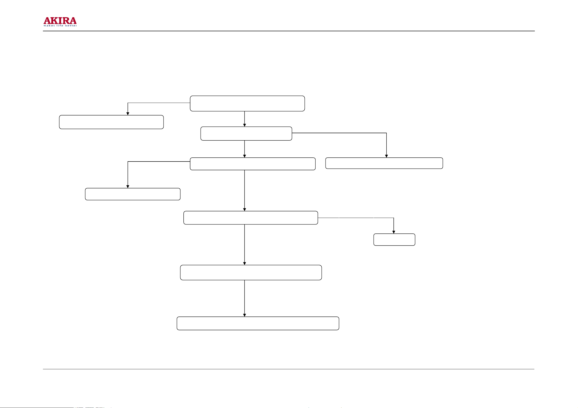
FAULT FINDING TREES
A Three-None(no raster, no picture, no sound)
This failure is mainly caused by big-power circuit such as power supply, horizontal scanning, vertical scanning.
The detail checking and repairing steps are as follow.
Voltage of C507
O
Check if V1513 collect-emitter
Was broken down
0V
Check XR502,F501,power
Swich, AC cord and plug
YES
Check V1513,V1512,F501,XR502,VD503
300V
Test voltage of V1513 base
0.6V
Check T501,VD1517,
C1515,C1517,V451,
Check if it get right
When cut off V504
VD522-VD529
C455,C456,T451
C467
Test the voltage of
301 pin1
CPU has sent the
Power-off signal
Check the voltage
of V1513 collector
0V
YES
4.5-5.5V
300V
1V
0V
0V
Check T501
Check V1513
0V
Check if V504
is broken down
Test the voltage of C528B
50V
Cut off R458
O
V
V
e
r
e
r
e
r
,
,
,
variation
v
o
l
v
o
l
v
o
2
4
V
2
4
V
2
4
V
t
a
g
e
t
a
g
e
l
t
a
g
e
s
,
a
n
d
,
a
n
d
,
a
n
T
T
T
e
s
t
o
t
h
e
s
t
o
t
h
e
s
t
o
t
h
1
8
8
V
1
8
8
1
8
a
a
8
s
s
a
s
LOW
VD525,VD1561,VR501,V542,
VD1517,V504,V1511
Check VD522,C528B
115V
Recover R458, unplug
XS403 for a While,then
test the voltage of C528B
o variation
Check V451,T451,T450,
Deflection coil
Check L452,VD436,C461
Deflection coil
115V
s
u
c
s
u
c
u
c
1
2
1
2
d
1
ormal
h
h
h
V
V
2
V
Check V451 pin C voltage
Check T451,V451,R458
130V
115V
301 pin39voltage
8V
301 pin33 voltage
2V
V450 pin C voltage
24V
Check R452,V450
Others
115V
Check R539,V1553,VD1561
504,V1511,V1512,R556
Others
Check N301,N401
0V
Check VD543,C525,
]R454,C453,T450,
C455,V451
0V
Check T451
Model No: 14THS3/CE.doc
Version 1.0
Page 12
12
N
N
N
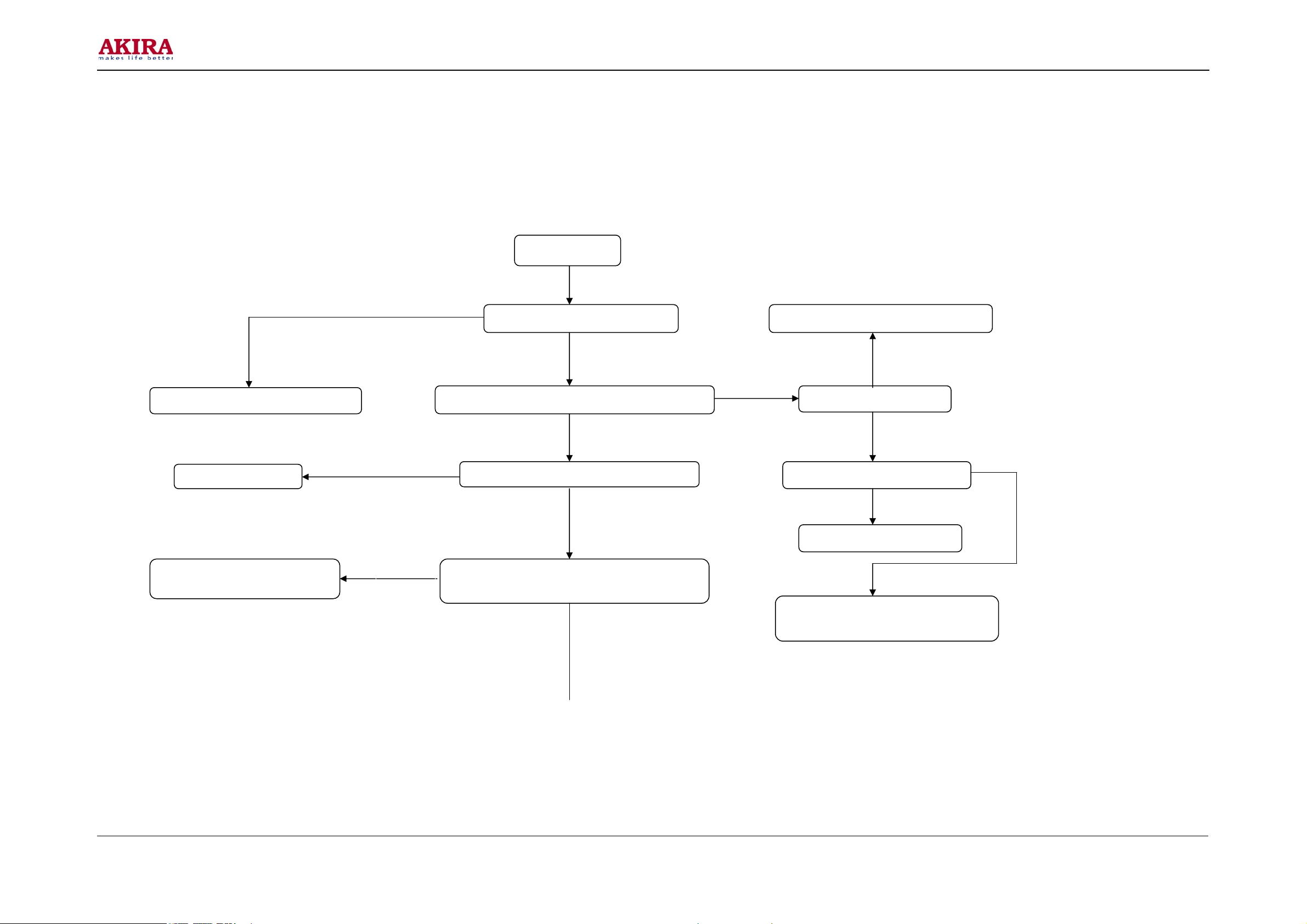
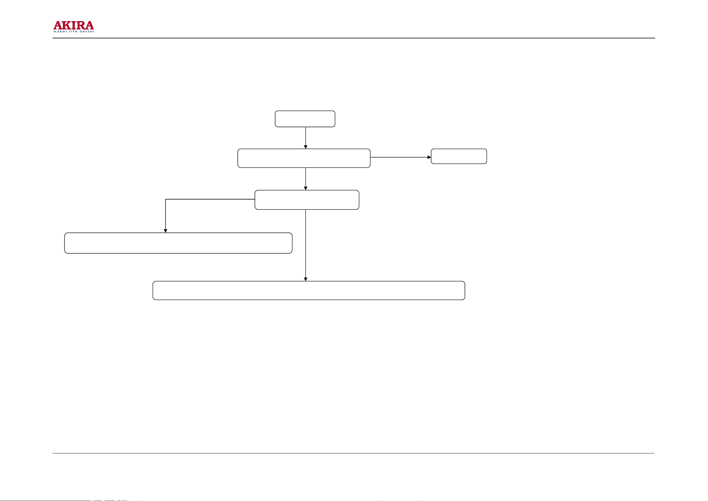
B Two-None (no picture, no sound)
The failure shows that the set does not display the picture but it has noise wave or blue background or OSD on the screen. This means that the circuits of power supply, horizontal scanning, vertical scanning
and video amplification are normal and they are not considered in the repairing. The failures are mainly in the small signal processing circuits.
Before checking these circuits, a kind of practical test method is introduced. It is called “Signal-input way ”. The detail is described as follow: We can use the resistance function of an analog multimeter,
connect the red pole (negative in ohm scope) on the circuit board ground, then touch softly the test point with another pole (black pole) in ohm scope meanwhile observe the reactivity on the output device.
Note : In the TV test, we mainly observe the noise wave on the CRT and listen to the noise voice liking as “Ka…..Ka” from the loudspeakers.
1. No picture
Check RF signal input and adaptor
Check N703, A101
Check R301,R302,
301,A101
O
Check if A101 has input signal
Check the “ VT ” voltage when auto searching
0V
Check the “ +5V ” voltage on A101
0V
The voltage between VL and BH vary from 0V to
5V or not when auto searching
No picture
YES
YES
Out of the “ 0-33V ” range
In the “ 0-33V ” range
5V
Check R703,N703,C703A
33V
The voltage on the C703
33V
o variation
Check the voltage on the C705
0-33V
Check R707, C707, A101
Check ,V701,N301, R701, R701A
,R704,R705,C701,C705,C706
Model No: 14THS3/CE.doc
Version 1.0
Page 13
13
N
N
N
NO NO N
Check R317, R318, R316,C307,A101,N301
Check,L331, C333, L752,C753A, L751, C751
Observe if there is snow-noise-wave disturbance on the CRT via using “Signal-input way ” by touching pin 23 and pin 24 of N301
YES
Observe if there is snow-noise-wave disturbance on the CRT via using “ Signal-input way ” by touching pin 38 of N301
Observe if there is snow-noise-wave disturbance on the CRT via using “Signal-input way ”by touching pin 17 of N301
Observe if snow-noise-wave disturbance on the CRT via using “ signal-input way ”by touching pin 40 of N301
Check if voltage on pin 31 of N301 is 1.7V
≥2V
Check C323,A101,N301
2V
Exam the voltage of “ AGC ” on A101 without antenna
3.8V
0V
Test the voltage on pin 14, 54, 56of N301
8V
Test the voltage on pin 51, 52, 53, 50 of N301
5V
O
O
Test if there is the sync signal on the pin 39 of N301
O
Check C361,C362,L361,N301
Observe if these is snow-noise-wave disturbance on the CRT via using “ Signal-input way ” by touching pin 51,52,53 of N301
Check R381,R382,R383,V912,V922,V932,N301
0V
YES
Check N503, N301,C532, R565,C524,
,VD561,V542
YES
Check N505, N301
YES
Check R331,C336,C337
YES
Check V351,V352,L351,Z351,C364
O
Model No: 14THS3/CE.doc
Version 1.0
Page 14
14
NO N
N
N
N
N
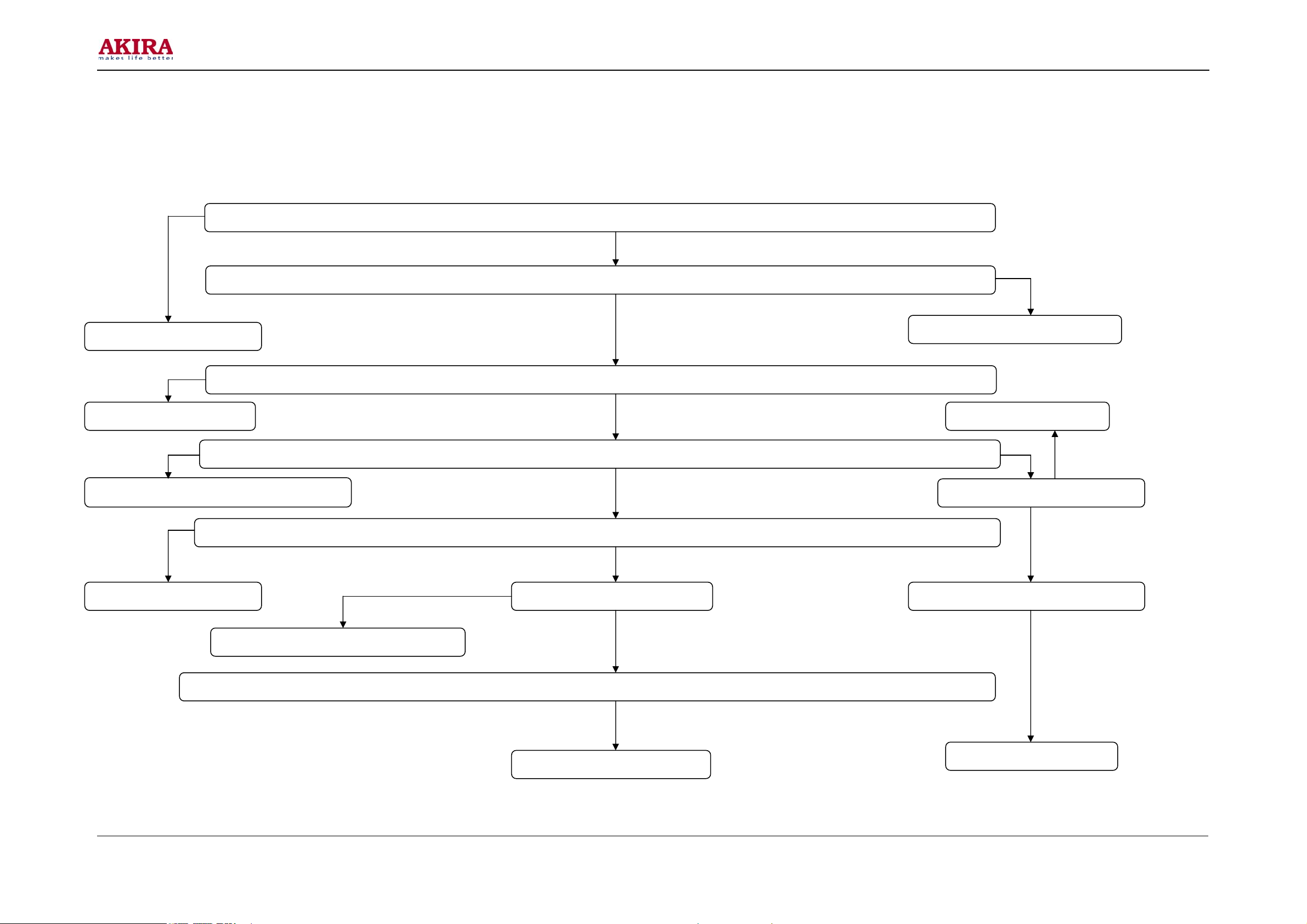
5. No sound
In this kind of failure, first of all we should observe if there is the picture on the CRT. It proves the small signal circuit to work correctly with the picture on the CRT and we only check the sound signal
processing and sound amplification circuit. The repairing method(B1) may be referred without picture. The detail checking and repairing steps are as follow.
Note:
Before repairing, assure that the volume is on and the state of set is in “TV” .
Check R733, C732, N301
Check R157,C157,N161
Check R153,C153,R154,C154,N121
Check C157,C153, N101
YES
YES
Hear if there is the voice liking “Ka…Ka ” in the loudspeaker via using “ Signal-input way ” by touching pin 7 of N301
O
Hear if there is the voice liking “Ka…Ka ” in the loudspeaker via using “ Signal-input way ” by touching pin 44 of N301
O
YES
YES
Hear if there is the voice liking “Ka…Ka ” in the loudspeaker via using “ Signal-input way ” by touching pin 3 of N121
O
Hear if there is the voice liking “Ka…Ka ” in the loudspeaker via using “ Signal-input way ” by touching pin 13 of N121
O
Hear if there is the voice liking “Ka…Ka ” in the loudspeaker via using “ Signal-input way ” by touching pin 6,8of N161
5V
The voltage on pin 1 of N701
Check VD521,R165,C522,T501,N161
Hear if there is the voice liking “Ka…Ka ” in the loudspeaker via using “ Signal-input way ” by touching pin 2,10 of N701
Check SP161, SP162, N161
12.5V
O
YES
Check C367,R369,V395,N301
Check 8V-power supply
YES
8V
The voltage on pin 16 of N121
8V
The voltage on pin 9,10of N121
8V
Check R126,N505, N121
Model No: 14THS3/CE.doc
Version 1.0
Page 15
15
N
N
N
C Only horizontal line in the middle of the screen:
If vertical deflection circuit does not work, this kind of failure will happen. In deflection yoke, there only has horizontal sweeping , the electron beam in the CRT only moves in the horizontal orientation , so
form this failure.
(While checking horizontal and vertical deflection circuit’ s failure , we have better to use an oscilloscope.)
Check C401,C402,R401,R402,N301
Check R405, C408, N401, N301
Abnormal
Abnormal
The waveform on the pin 21,22 of N301
ormal
The voltage on pin 2 of N401
24V
Measuring the waveform on pin 1 of N401
ormal
Measuring the waveform on pin 5 of N401
ormal
Measuring the waveform on the deflection yoke
Abnormal
Check R407,C408,R406,XS403, deflection yoke
0V
Check VD470, R470,VD401,N401
The deflection yoke on the CRT
Abnormal
Check N402
Model No: 14THS3/CE.doc
Version 1.0
Page 16
16
N
N
D Only vertical line in the middle of the screen
This is a dangerous failure. It probable causes flashover and smoking inside the set. Don’ t let your TV work for a long time as this failure appears. Because the electron beam can not move in the horizontal
orientation, the failure should be in the horizontal deflection circuit. We mainly check the open-circuit fault in horizontal deflection circuit. The detail checking and repairing steps are as follow:
Check if there is bad solder between XS403, and the main board
E UOC does not work
In television, remote-control system is similar with the computer system. In theory , it can work if it holds two conditions as follow:
1) The power supply: In general, it is 5V, the error is not above 10% and the disturbance pulse is as small as possible.
2) The clock pulse: In TDA93XX circuit, the clock pulse is generated by pin58 / pin59 of N301 and 12M crystal oscillator.
Television’ s remote-control system also needs reset circuit that can preset the values in internal register. The circuit around pin57
of N204 is called auto-reset circuit. If UOC detects errors in resetting, it will come to the state of programme protected.
Model No: 14THS3/CE.doc
Version 1.0
Check L452, VD436, C467,C455,especial in inductive components and connector
YES
The horizontal yoke is opened or not
Whether “ XS403” is opened
Vertical line
YES
Repair CRT
O
O
Page 17
17
N
N
N
N
The detail checking and repairing steps are as follow:
O
Observe if there is sine wave on the pin 58 or pin 59
of N301 with an oscilloscope
The voltage on the pin 56 of N301
301 does not work
3.3V 3.3V
Check the voltage on the positive pole of C548
=3.3V
Check X761, N301
Check N301
F No OSD (On Screen Display)
This failure is usually cause by the circuit of character generated and located. Most of reasons are that the horizontal and vertical flyback pulse signals do not come to UOC.
We can judge this failure by measuring the wave of the character in an oscilloscope.
The detail checking and repairing steps are as follow:
3.3V
Check the voltage on the pin 54 of N301
Check L752,L753
YES
3.3V
Check the voltage on the emitter of VD564
3.3V
No OSD
Check the wave on the pin 7 of FBT
O
Check FBT T451
3.3V
Check VD522, T501
Check alternant voltage on secondary coil of N505,
YES
Check T501, VD522,R565
Check the voltage on the positive pole of VD522
3V
YES
Check C482, R485, VD483, R487, N301
=14V
O
Check R561,VD564
Check R565,R546,N505
Model No: 14THS3/CE.doc
Version 1.0
Page 18
18
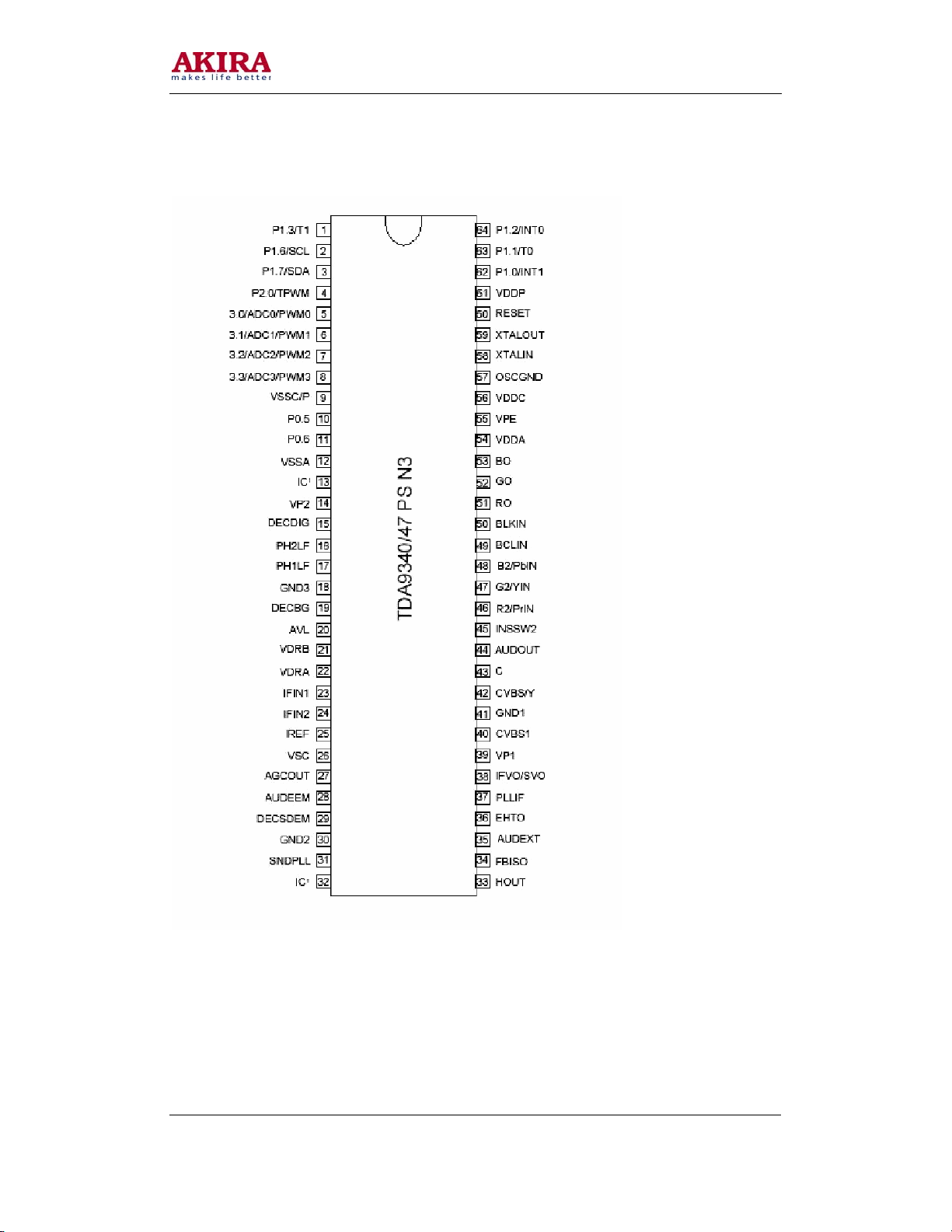
IC BLOCK DIAGRAM
Fig 1: OM8370 Illustration
Model No: 14THS3/CE.doc
Version 1.0
Page 19
19
MAIN CHIP INSTRUCTION
Pin 1 Standby control, “1” is on, “0” is off.
Pin 2 SCL
Pin 3 SDA
Pin 4 Tuning PWM output
Pin 5 Auto AV control SW, connected with the SCART 8th pin. Input. The rising edge or
the falling edge operates.
Pin 6 Key board input.
Pin 7 Volume
Pin 8 Mute control, “1” is mute, “0” is off.
Pin 9, Pin 12,
Pin 18, Pin 30,
Pin 35, Pin 41,
Pin 55
Pin 10 BAND 1 control output.
Pin 11 BAND 2
Pin 13 SECAM PLL, connected with a capacitance (no use in this type).
Pin 14 +8V power source supply
Pin 15 Using a capacitor of 220n in series to GND. This pin decouples the internal digital
Pin 16 Phase-2 control loop, this pin requires a capacitor at 2.2nF © in series to GND.
Pin 17 Phase-1 control loop filter connected to pin 17 is suitable for various signal
Pin 18 GND
Pin 19 Bandgap decoupling, the bandgap circuit provides a very stable and temperature
Pin 20 East-west pillow signal output.
Pin 21, Pin 22 Vertical drive output.
Pin 23, Pin 24 IF input.
Pin 25 Reference current/ This pin requires a resistor to ground. The optimal reference
Pin 26 Vertical sawtooth. This pin requires a capacitor to ground of 100nF.
Pin 27 AGC output. This output is used to control (reduce) the tuner gain for strong RF
Pin 28 Audio de-emphasis.
Pin 29 Sound decoupling. This pin requires a capacitor connected to ground. The pin acts
Pin 30 GND
Pin 31 Sound loop filter.
Pin 32 AVL filter
Pin 33 Horizontal drive signal output, needs a resistor in series to +8V.
Pin 34 Sandcastle output /flyback input.
Pin 35 External audio input, this pin should be grounded in this chassis.
GND
supply voltage of the video process and minimizes the disturbance to the sensitive
analogue parts.
conditions like strong /weak and VCR signal. This is achieved by switching of the
loop filter time constant by changing the Phase-1 output current.
independent reference voltage. This reference voltage (4.0V) ensures optimal
performance of the analogue video processor part of the OM8370 and is used in
almost all functional circuit blocks.
current is 100mA which is determined by this resistor. The 100mA reference
current should not be changed because the geometry processor is optimized for this
current. Furthermore the output current of vertical drive and EW are proportional to
this current.
signals.
as a low pass filter needed for the DC feedback loop.
Model No: 14THS3/CE.doc
Version 1.0
Page 20
20
Pin 36 EHT tracking /over voltage protection. If something is wrong, the anode high
voltage rise the heater voltage will rise too. When the rising voltage arrive some
limit, the V406 works, the voltage of pin 36 will exceed 3.9V. The OM8370 will
stop working.
Pin 37 PLL loop filter.
Pin 38 CVBS output. Monitor or RF videos can be selected.
Pin 39 +8V supply source
Pin 40 CVBS input
Pin 42 Y signal input
Pin 43 C signal input
Pin 44 Main audio output. This pin is connected to the TDA9859.
Pin 45 RGB signal input blanking.
Pin 46, Pin 47,
Pin 48
Pin 49 ABL. It means been current limiter input. R410 is the control resistor.
Pin 50 Black current input from the CRT board.
Pin 51, Pin 52,
Pin 53
Pin 54 +3.3V
Pin 55 GND
Pin 56 +3.3V
Pin 57, Pin 58,
Pin 59
Pin 60 Reset. NC in this chassis
Pin 61 +3.3V
Pin 62 NC
Pin 63 This pin is connected to the HEF4094. Functions expending.
Pin 64 IR signal input.
RGB signal input.
RGB drive signal output to the CRT board.
12MHz crystal
Model No: 14THS3/CE.doc
Version 1.0
Page 21

21
Fig 2: HEF4052BP Illustration
Model No: 14THS3/CE.doc
Version 1.0
Page 22

22
FUNCTION TABLE OF N4052
Input
Ē
L L L Y0A – ZA; Y0B – ZB
L L H Y1A – ZA; Y1B – ZB
L H L Y2A – ZA; Y
L H H Y3A – ZA; Y3B – ZB
H X X NONE
Notes:
H = HIGH state (the more positive voltage)
L = LOW state (the less positive voltage)
X = state is immaterial
A
1
A0
Channel On
2B
– ZB
Model No: 14THS3/CE.doc
Version 1.0
Page 23

23
IC N402 <VERTICAL OUTPUT> LA78040 (or STV9302)
Model No: 14THS3/CE.doc
Version 1.0
Page 24

24
Model No: 14THS3/CE.doc
Version 1.0
Page 25

25
Model No: 14THS3/CE.doc
Version 1.0
Page 26

26
Model No: 14THS3/CE.doc
Version 1.0
Page 27

27
Model No: 14THS3/CE.doc
Version 1.0
Page 28

28
Model No: 14THS3/CE.doc
Version 1.0
Page 29

29
Model No: 14THS3/CE.doc
Version 1.0
Page 30

30
Model No: 14THS3/CE.doc
Version 1.0
Page 31

31
Model No: 14THS3/CE.doc
Version 1.0
Page 32

32
Model No: 14THS3/CE.doc
Version 1.0
Page 33

33
Model No: 14THS3/CE.doc
Version 1.0
Page 34

34
Model No: 14THS3/CE.doc
Version 1.0
Page 35

35
1 Inverting input
2 Vcc
3 Pump up out
4 GND
5 VER output
6 Output stage Vcc
7 Non inv. Put
Model No: 14THS3/CE.doc
Version 1.0
Page 36

36
Fig 4 AN7522N Illustration
Model No: 14THS3/CE.doc
Version 1.0
Page 37

37
Model No: 14THS3/CE.doc
Version 1.0
Page 38

38
Model No: 14THS3/CE.doc
Version 1.0
Page 39

39
Fig 5: KA5Q0765RT Illustration
Model No: 14THS3/CE.doc
Version 1.0
Page 40

40
FACTORY MENU
Main power +B setting
Receive standard color pattern RF signal. Set picture to “Standard Mode”. Adjust VR501, to get +B
(VD542 -) voltage =110V.
I2C bus control adjustment method
How to enter and exit factory mode (with customer’s remote controller)
1. Press [menu] key → display picture menu
2. Press digital key “6” “4” “8” “3” → display “M”
3. Push [standby] key one time to exit factory mode and return to normal.
How to select menus in factory mode
In factory mode {“M” mode) there are ten menus totally. Menu 1 to Menu 4 can be selected directly
but Menu 5 to Menu 0 must be select by these steps:
1. Press “CALL” key, to call “M”.
2. Press “LOCK” key, then press any one numeric key from 5 to 0.
For example, to select Menu 7, you should press “call” key and LOCK key in turns, then press the
numeric key 7.
Menu function introduction
Menu 1
Item
V SLOPE 32 32 Vertical linearity
V SHIFT 32 32 Vertical position
V SIZE 32 32 Vertical size
V SC 32 32 Vertical S correction
H SHIFT 32 32 Horizontal position
Menu 2
Item Preset value Definition
RF AGC 20 RF AGC adjust, when the signal is poor, you can decrease the
Shipping For factory use
Menu 3
Item Preset value Definition
BT 75 Bright in W/B mode
CT 75 Contrast in W/B mode
SC Screen mode (press Vol +/- or CH +/- key to enter or exit).
RB 32 Red bias adjust
GB 32 Green bias adjust
RD 32 Red drive adjust
GD 32 Green drive adjust
BD 32 Blue drive adjust
SB 40 Sub-bright adjust
Note:
1. BT /CT can not be remembered.
2. RB /GB /RD /GD /BD /SB can be remembered.
Model No: 14THS3/CE.doc
Version 1.0
Preset value
50Hz 60Hz
value to increase the gain
Adjust screen knob on FBT to adjust the bright of the line.
Definition
Page 41

41
Menu 4
Item
OSD V 32 32 OSD vertical position
OSD H 32 32 OSD horizontal position
Menu 5
Item Preset value Definition
MODE STANDARD Picture mode selection. You can select four modes:
BRIGHT 75 Preset bright value for the mode you have selected above.
CONTRAST 75 Preset contrast value.
COLOR 50 Preset color value.
SHARP 50 Preset sharpness value f.
SC BRIGHT 20 Preset bright value for screen mode.
COOL 10 The off set in cool mode.
WARM 10 The off set in bright mode.
Y DELAY PAL 8 Y signal delay in PAL system.
Y DELAY NTSC 8 Y signal delay in NTSC system.
Y DELAY AV 8 Y signal delay in AV mode.
Menu 3
Item Preset value Definition
OSO 1 Over scan switch Off.
AGC SPEED 1 0: Slow AGC action. IF –AGC capacitor is 3.1uF.
FFI 0 Fast filter IFPLL.
FSL 0
FMWS 0 FM search window width
RPO 1
NTSC MATRIX 0 0: JAPAN
IFS REDUCE 0 0: Decrease the sensitivity of IF while search.
VOL PIN 0 0: OC gate output
SOFT CLIP 0
PEAK WHITE 0
CORING 0
Preset value
50Hz 60Hz
STANDARD, VIVID, MILD and USER.
0: not available
1: available
1: Normal. IF –AGC capacitor is 2.2uF.
2: Fast AGC action. 3 times speed than normal.
3: Fast AGC action. 6 times speed than normal.
0: Normal
1: Fast
0: ±225KHz
1: ±450KHz
1: USA
1: Not decrease the sensitivity of IF while search.
1: PULL-PUSH output
Definition
Model No: 14THS3/CE.doc
Version 1.0
Page 42

42
Menu 7
Item Preset value Definition
IFFS 38.9MHz IF Frequency selection
DK OFF DK system selection
I OFF I system selection
BG ON BG system selection
M OFF M system selection
SIF PRI ON SIF Priority
AV2 ON AV2 selection
S-VIDEO ON S-video selection
YUV ON YUV selection
VOL ADJ POINT 1 VOL curve point selection
VOL ADJ VALUE 10 VOL curve value adjusting on the selected point
Menu 8
Item Preset value Definition
CATHODE 4 Cathode adjusting From 0 to 15
UOC VOL 0 Must be 0. When set 1, AV volume will be abnormal
FM ATT 45 UOC output volume adjusting. From 0-63
CHINESE 1 Chinese OSD selection
Menu 9
Item Preset value Definition
BAND 2 Must be 2 according to be TUNER
START ON 0 0: Last memory mode: TV mode
1: Power on standby mode.
LOGO OFF No use
ON DELAY 10 Power on delay time adjust
ON DELAY M 5 Preset on delay time
CURTAIN OFF
OSD FORM 0 From 0 to 3
AV MEM ON AV memory
BLUE SCREEN ON Off: Black screen
On: Blue screen
S_VHS SW 1/0 S-VHS switch
0: S-VHS is independent
1: S-VHS is paralleled to AV1
OFF-SET 32 IF demodulator OFF-SET value. The default value is 32.
Menu 0
Item Preset value Definition
SUB CON 63 SUB CONTRAST
SUB COLOR 63
SUB SHARP 63
SUB TINT 63
FS MODE 0 FS TUNER (No use)
FS-VL-H 0 Frequency point setting in FS MODE (No use)
FS-VL-L 0 Frequency point setting in FS MODE (No use)
FS-VH-H 0 Frequency point setting is FS MODE (No use)
FS-VH-L 0 Frequency point setting in FS MODE (No use)
Model No: 14THS3/CE.doc
Version 1.0
Page 43

43
EXPLODED VIEW AND PART NAME
Model No: 14THS3/CE.doc
Version 1.0
Page 44

44
BOM LIST
Ref.No
Name Specification
1 CARBON RES RT13-1/6W-10Ω-J D10B100J-T RDB100J-NAAT 2 R312、871
2 CARBON RES RT13-1/6W-22Ω-J D10B220J-T RDB220J-NAAT 3 R914、924、934
3 CARBON RES RT13-1/6W-33Ω-J D10B330J-T RDB330J-NAAT 2 R398、806
4 CARBON RES RT13-1/6W-47Ω-J D10B470J-T RDB470J-NAAT 5 R368、708、911、921、931
5 CARBON RES RT13-1/6W-56Ω-J D10B560J-T RDB560J-NAAT 2 R354、355
6 CARBON RES RT13-1/6W-68Ω-J D10B680J-T RDB680J-NAAT 1 R304
7 CARBON RES RT13-1/6W-75Ω-J D10B750J-T RDB750J-NAAT 1 R801
8 CARBON RES RT13-1/6W-82Ω-J D10B820J-T RDB820J-NAAT 1 R313
9
CARBON RES RT13-1/6W-100Ω-J D10B101J-T RDB101J-NAAT 19
10 CARBON RES RT13-1/6W-150Ω-J D10B151J-T RDB151J-NAAT 3 R815A、848、852
11 CARBON RES RT13-1/6W-180Ω-J D10B181J-T RDB181J-NAAT 1 R353
12 CARBON RES RT13-1/6W-220Ω-J D10B221J-T RDB221J-NAAT 4 R311、917、927、937
13 CARBON RES RT13-1/6W-300Ω-J D10B301J-T RDB301J-NAAT 3 R913、923、933
14 CARBON RES RT13-1/6W-330Ω-J D10B331J-T RDB331J-NAAT 4 R805、916、926、936
Components EASTKIT EAST KIT
Q'TY Parts Location
Parts Code Parts Code
R301、302、359、363、365
R366、381、382、383、401
R402、452、723、724、743
R815、824、861、862
Model No: 14THS3/CE.doc
Version 1.0
Page 45

45
Ref.No
Name Specification Parts Code Parts Code
16 CARBON RES RT13-1/6W-470Ω-J D10B471J-T RDB471J-NAAT 2 R308、1517
17 CARBON RES RT13-1/6W-680Ω-J D10B681J-T RDB681J-NAAT 2 R316、482
18 CARBON RES RT13-1/6W-1KΩ-J D10B102J-T RDB102J-NAAT 14
19 CARBON RES RT13-1/6W-1.2KΩ-J D10B122J-T RDB122J-NAAT 2 R305、560
20 CARBON RES RT13-1/6W-1.5KΩ-J D10B152J-T RDB152J-NAAT 2 R397、732
21 CARBON RES RT13-1/6W-1.8KΩ-J D10B182J-T RDB182J-NAAT 3 R403、405、1523
CARBON RES RT13-1/6W-2.2KΩ-J D10B222J-T RDB222J-NAAT
23 CARBON RES RT13-1/6W-2.7KΩ-J D10B272J-T RDB272J-NAAT 1 R321
CARBON RES RT13-1/6W-3.3KΩ-J D10B332J-T RDB332J-NAAT
25 CARBON RES RT13-1/6W-3.9KΩ-J D10B392J-T RDB392J-NAAT 2 R455、462
CARBON RES RT13-1/6W-4.7KΩ-J D10B472J-T RDB472J-NAAT
27 CARBON RES RT13-1/6W-5.6KΩ-J D10B562J-T RDB562J-NAAT 3 R370、540、1511
28 CARBON RES RT13-1/6W-8.2KΩ-J D10B822J-T RDB822J-NAAT 2 R153A、157A
Components EASTKIT EAST KIT
Q'TY Parts Location
R128、129、369、460、464
R481、701、734、802、803
R816、818、825、827、
R315、351、361、371、451 22
6
R463
R310、721、722、728、735 24
9
R736、737、741、742
10
R131、133、154、158、306 26
R309、360、362、733、731
Model No: 14THS3/CE.doc
Version 1.0
Page 46

46
Ref.No
Name Specification Parts Code Parts Code
29 CARBON RES RT13-1/6W-10KΩ-J D10B103J-T RDB103J-NAAT 24
30 CARBON RES RT13-1/6W-15KΩ-J D10B153J-T RDB153J-NAAT 1 R331
31 CARBON RES RT13-1/6W-22KΩ-J D10B223J-T RDB223J-NAAT 5
32 CARBON RES RT13-1/6W-27KΩ-J D10B223J-T RDB273J-NAAT 2 R484、487
33 CARBON RES RT13-1/6W-33KΩ-J D10B333J-T RDB333J-NAAT 4 R171、175、317、385
34 CARBON RES RT13-1/6W-47KΩ-J D10B473J-T RDB473J-NAAT 3 R172、732A、745
CARBON RES RT13-1/6W-56KΩ-J D10B563J-T RDB563J-NAAT 1 R319
35 CARBON RES RT13-1/6W-68KΩ-J D10B683J-T RDB683J-NAAT 1 R173
36 CARBON RES RT13-1/6W-82KΩ-J D10B823J-T RDB823J-NAAT 1 R314
37 CARBON RES RT13-1/6W-100KΩ-J D10B104J-T RDB104J-NAAT 5 R350、483、802A、803A、807
38 CARBON RES RT13-1/6W-150KΩ-J D10B154J-T RDB154J-NAAT 1 R318
39 CARBON RES RT13-1/6W-270KΩ-J D10B274J-T RDB274J-NAAT 1 R174
40 CARBON RES RT13-1/6W-560KΩ-J D10B564J-T RDB564J-NAAT 1 R465
41 CARBON RES RT14-1/4W-1.0Ω-J D10C1R0J-T RDC1R0J-NABT 1 R404
Components EASTKIT EAST KIT
Q'TY Parts Location
R126、127、163、380、395
R396、434、461、548、551
R704、705、706、707、709
R816A、818A、825A、827A
R851A、852A、912、922、932
R162、384、804
R1515、1556、
Model No: 14THS3/CE.doc
Version 1.0
Page 47

47
Ref.No
42 CARBON RES RT14-1/4W-2.7Ω-J D10C2R7J-T RDC2R7J-NABTD 1 R468
43 CARBON RES RT14-1/4W-22Ω-J D10C220J-T RDC220J-NABTD 1 R513
44 CARBON RES RT14-1/4W-27Ω-J D10C270J-T RDC270J-NABTD 1 R561
45 CARBON RES RT14-1/4W-2.2KΩ-J D10C222J-T RDC222J-NABT 2 R161、1526、
46 CARBON RES RT14-1/4W-10KΩ-J D10C103J-T RDC103J-NABT 1 R485
47 CARBON RES RT14-1/4W-15KΩ-J D10C153J-T RDC153J-NABTD 1 R1522
48 CARBON RES RT14-1/4W-51KΩ-J D10C513J-T RDC513J-NABT 2 R539、539A
49 CARBON RES RT14-1/4W-150KΩ-J D10C154J-T RDC154J-NABTD 1 R1554
50 CARBON RES RT14-1/4W-330KΩ-J D10C334J-T RDC334J-NABTO 1 R942
51 CARBON RES RT15-1/2W-270Ω-J D10D271J-T RDD271J-NACT 1 R407
52 CARBON RES RT15-1/2W-1KΩ-J D10D102J-T RDD102J-NACT 1 R453
53 CARBON RES RT15-1/2W-47KΩ-J D10D473J-T RDD473J-NACTD 1 R1555
54 CARBON RES RT15-1/2W-120KΩ-J D10D124J-T RDD124J-NACTD 2 R507、1520、
55 FUSE RES RF10-1/2W-1.0Ω-J F10D1R0J-C RFD1R0J4ACCN 1 R473B
56 FUSE RES RF10-1W-0.47Ω-J 4 R470、472、555、565
57 FUSE RES RF10-1W-1Ω-J 1 R566
Components EASTKIT EAST KIT
Q'TY Parts Location
Name Specification Parts Code Parts Code
FUSE RES RF10-1W-0.27Ω-J 1 R165、
Model No: 14THS3/CE.doc
Version 1.0
Page 48

48
Ref.No
58 FUSE RES RF10-2W-3.9Ω-J 1 R480
59 OXIDE FILM RES RY16-1W-1.5Ω-J S10E1R5J-C RSE1R5J5DCCN 1 R406
60 OXIDE FILM RES RY16-1W-22Ω-J S10E220J-C RSE220J5ACCN 1 R300A
61 OXIDE FILM RES RY16-1W-1KΩ-J S10E102J-C RSE102J4ACCN 1 R466
62 OXIDE FILM RES RY17-2W-5.6Ω-J S10F5R6J-C RSF5R6J5ACDN 1 R941
63 OXIDE FILM RES RY17-2W-56Ω-J S10F560J-C RSF560J5ACDN 1 R530
64 OXIDE FILM RES RY17-2W-270Ω-J S10F271J-C RSF271J7ACDN 2 R454、546
65 OXIDE FILM RES RY17-2W-10KΩ-J S10F103J-C RSF103J5ACDN 1 R467
66 OXIDE FILM RES RY17-2W-12KΩ-J S10F123J-C RSF123J7ACDN 3 R915、925、935
67 OXIDE FILM RES RY17-2W-22KΩ-J S10F223J-C RSF223J7ACDN 1 R556
68 RESISTOR METAL RJ13-1/6W-39KΩ-F RJB393F-NAAF 1 R411
69 Glass-Glazed RES RI40-1/2W-1.5KΩ-J C10D152K-T RGDX152K-03N 3 R918、928、938
70 Glass-Glazed RES RI40-1/2W-24MΩ-K C10D246K-T RGDX246K-03N 1 R519
71 Thermal RES PTC MZ72 180HM P10X180J-C
72 WIRE RES RX27-3A-5W-1.8Ω-K W10J1R8K RWH1R8K5AF-N 1 XR502
73 WIRE RES RXG6-5W-3.9Ω-K W11H3R9K RWH3R9K4AK-N 1 R458
74 WIRE RES RX27-5W-27Ω-K W11H270K
75 WIRE RES RX27-3A-5W-68Ω-K W11H680K RWH680K4AK-N 1 R504
Components EASTKIT EAST KIT
Name Specification Parts Code Parts Code
OXIDE FILM RES RY17-2W-12KΩ-J 1 R703
DH1180M001-
NC 1 PS501
RWH270K7AJ-
NF
Q'TY Parts Location
1 R1524
Model No: 14THS3/CE.doc
Version 1.0
Page 49

49
Ref.No
76 VARIABLE RES WI06-2AA-2KΩ V11D202B VDAAA202A001C 1 VR501
77 CERAMIC CAPA. CC1-06A-CH-63V-33pF-J C2CF330J-T CCF330JICA-F 2 C761、762
78
79 CERAMIC CAPA. CT1-06A-2B4-63V-330pF-K C2BF331K-T 3 C911、921、931
80 CERAMIC CAPA. CT1-06A-2B4-63V-470pF-K C2BF471K-T 7
81 CERAMIC CAPA. CT1-06A-2B4-63V-560pF-K C2BF561K-T 1 C381
82 CERAMIC CAPA. CT1-06A-2B4-63V-820pF-K C2BF821K-T 1 C323
83 CERAMIC CAPA. CT1-06A-2B4-63V-1000pF-K C2BF102K-T CKF102K1BA-F 7
84 CERAMIC CAPA. CT1-06A-2B4-63V-2200pF-K C2BF222K-T CKF222K1BA-F 1 C335
85 CERAMIC CAPA. CT1-06A-2B4-63V-4700pF-K C2BF472K-T CKF472K1BA-F 2 C324、336
86 CERAMIC CAPA. CT1-08A-2F4-63V-0.01uF-Z C2FF103Z-T CKF103Z1FA-F 15
87 CERAMIC CAPA. CT1-08C-2B4-500V-220pF-K C2BP221K-T CKP221K1BA-N 1 C405
88 CERAMIC CAPA. CT1-08C-2B4-500V-1000pF-K C2BP102K-T CKP102K1BA-F 1 C452
89 CERAMIC CAPA. CT1-08C-2B4-500V-3900pF-K C2BP392K-T CKP392K1BA-F 1 C451
Components EASTKIT EAST KIT
Q'TY Parts Location
Name Specification Parts Code Parts Code
C803、805、812、814
C824、826
C732、
C308、311、401
C402、481、721、861
C162、302、309、312、313
C332、362、472、475、535
C703A、723、744、752、756
Model No: 14THS3/CE.doc
Version 1.0
Page 50

50
Ref.No
90 CERAMIC CAPA. CT81-08C-2R-1KV-470pF-K C2RW471K-O CKW471K2RA-N 1 C529
91 CERAMIC CAPA. CT81-08C-2R-1KV-1000pF-K C2BW102K-O CKW102K2BJ-N 4 C503、504、505、506
92 CERAMIC CAPA. CT81-08C-2R-2KV-220pF-K C2RX221K-O CKX221K2RA-N 1 C527
93 CERAMIC CAPA. CT81-08C-2R-2KV-470pF-K C2RX471K-O CKX471K2RA-N 2 C456、543
94 CERAMIC CAPA. CT81-08C-2R-2KV-680pF-K C2RX681K-O CKX681K2RA-N 1 C509
95 CERAMIC CAPA. CT81-08C-2R-2KV-1000pF-K C2RX102K-O CKX102P2EJ-N 1 C943
96 CERAMIC CAPA. CK-400V-470PF-±20% C2EM471M-O CKMX471K301N 2 C515A、598
97 CERAMIC CAPA. CK-400V-1000PF-±20% C2EM102M-O CKMX102M301N 1 C515
98 CERAMIC CAPA. CD110-10V-100uF -M E10C100M-T CEB101MYACBN 1 C548
99 Electrolytic CAPA. CD110-16V-10uF -M E20C100M-T 12
100 Electrolytic Capa. CD110-16V-22uF -M E20C220M-T CEC220MYACAN 1 C745
101 Electrolytic Capa. CD110-16V-47uF -M E20C470M-T CEC470MYACAN 8
102 Electrolytic Capa. CD110-16V-100uF -M E20C101M-T CEC101MYACBN 2 C361、743
103 Electrolytic Capa. CD110-16V-470uF -M E20C471M-T CEC471MYACCN 3 C525、532、801
104 Electrolytic Capa. CD110-25V-100uF -M E20D101M CED101MYACBN 5 C406、471、471A、474、474A
105 Electrolytic Capa. CD110-25V-470uF -M E20D471M CED471MYACBN 1 C161
Components EASTKIT EAST KIT
Q'TY Parts Location
Name Specification Parts Code Parts Code
C163A、172、301、307、322
C363、364、367、751、807
C841、871
C116、171、333、352、561、
C723A、811、823
Model No: 14THS3/CE.doc
Version 1.0
Page 51

51
Ref.No
106 Electrolytic Capa. CD110-25V-1000uF -M E20D102M CED102M1ACHN 1 C522
107 Electrolytic Capa. CD110-25V-2200uF -M E20D222M CED222M1ACKN 1 C524
108 Electrolytic Capa. CD110-35V-47uF -M E20E470M-T CEE470MYACCN 1 C453
109 Electrolytic Capa. CD110-35V-330uF -M E20E331M CEE331M1ACFN 1 C530
110 Electrolytic Capa. CD110-50V-0.47uF -M E20FR47M-T CEFR47MYACAN 5 C121、123、340(MI)、372、374
111 Electrolytic Capa. CD110-50V-1uF -M E20F1R0M-T CEF1R0MYACAN 11
112 Electrolytic Capa. CD110-50V-2.2uF -M E20F2R2M-T CEF2R2MYACAN 2 C339、755
113 Electrolytic Capa. CD110-50V-4.7uF -M E20F4R7M-T CEF4R7MYACAN 5 C303、304、325、353、464
114 Electrolytic Capa. CD110-50V-22uF -M E20F220M-T CEF220MYACBN 1 C703
115 Electrolytic Capa. CD110-50V-47uF -M E20F470M-T CEF470MYACBN 1 C462
116 Electrolytic Capa. CD112A-160V-4.7uF -M E20H4R7M CEH4R7MYBCCN 1 C466
117 Electrolytic Capa. CD110-160V-10uF -M E20H100M CEH100M1ACEN 1 C458
118 Electrolytic Capa. CD288-160V-100uF -M E20H101M CEH101M2ECKN 1 C528B
119 Electrolytic Capa. CD288H-250V-10uF-M E21K100M CEK100M1ACHN 2 C477、941
120 Electrolytic Capa. CD293-400V-150uF-±10% 1 C507
121 FILM CAPA CL11-50V/63V-0.1uF-K F20F104K-T CAY104K1-H-F 4 C326、338、365、411
122 FILM CAPA CL11-50V/63V-0.22uF-K F20F224K-T CAY224K1-H-F 3 C331(MI)、334、404
Components EASTKIT EAST KIT
Q'TY Parts Location
Name Specification Parts Code Parts Code
C153、157、163、337、804、
C806、813、815、825、827
C862
Model No: 14THS3/CE.doc
Version 1.0
Page 52

52
Ref.No
123 FILM CAPA CL21X-50V-0.47u-K F22F474K-T CAY474K1-H-F 1 C461
124 FILM CAPA CL11-100V-3300pF-K F20G332K-T CFG332K1-H-N 1 C321
125 FILM CAPA CL11-100V-5600PF-J F20G562J-T CFG562J1-H-N 2 C154、158
126 FILM CAPA CL11-100V-0.012uF-J F20G123J-T CFG123J1-H-NW 1 C1515
127 FILM CAPA CL11-100V-0.022uF-J F20G223J-T CFG223J1-H-NW 1 C1517
128 FILM CAPA CL11-100V-0.033uF-K F20G333K-T CFG333K1-H-N 1 C403
129 FILM CAPA CL11-100V-0.047uF-K F20G473K-T CFG473K1-H-N 1 C1513
130 FILM CAPA CL11-100V-0.1uF-K F20G104K-T CFG104K2-H-N 5 C1514、460、705、706、707
131 FILM CAPA CBB21-200V-0.39uF±5% F20J394J CNJ394J9-H-N 1 C467
132 FILM CAPA CBB62-250VAC-0.22uF-M F20R224M CMLX224M901N 1 C501
133 FILM CAPA CBB81-1.6KV-7500PF-J 1 C455
134
135 INDUCTOR LGA0204-3.9uH-K L2X239K-T LBA3R9K----T 1 L351
136 INDUCTOR LGA0204-1uH-K L2X210K-T LBA1R0K----T 1 L302
137 INDUCTOR LGA0307-10uH-K L3X2100K-T LBB100K----T 5 L331、361、751、752、753
138 INDUCTOR LGA0307-22uH-K L3X2220K-T LBB220K-----T 1 L401
139 INDUCTOR LGA0307-82uH-K L3X2820K-T LBB820K-----T 3 L911、912、913
140 INDUCTOR Magnetic Coil LEA001-5----N 1 L450
141 PHOTO COUPLE PC817B/C RX0001XX NLTV817B----N 1 N504
Components EASTKIT EAST KIT
Q'TY Parts Location
Name Specification Parts Code Parts Code
Coil And
Inductance 北塔LX036,利通LX36 1 L452
Model No: 14THS3/CE.doc
Version 1.0
Page 53

53
Ref.No
142 DIODE 1S1555/IN4148 DR0001XX-T DRIN4148---T 13
143 DIODE BAV21 DRBAV21----BP 3 VD912、922、932
144 RECTIFIER DIODE FR105/RGP10D DR0003XX-T DRRGP10D---T 5 VD401、470、471、525、1517
145 DIODE TVR4N DR0015XX-T DRTTVR4N---NZ 4 VD503、504、505、506
146 RECTIFIER DIODE RGP10J DR0017XX DRRGP10J---T 3
147 RECTIFIER DIODE RGP15D DRRGP15D----N 2 VD521、543
148 DIODE ZENER HZ5C1 DZ0002XX-T DZHZ5C1----T 1 VD300A
149 DIODE ZENER HZ22-2 DZHZ22-2---T 1 VD481
150 DIODE ZENER HZ3C3 DZHZ3C3-----T 1 VD564
151 DIODE ZENER HZ6C2 DZHZ6C2----TD 1 VD1561
152 DIODE ZENER HZ7C1 DZHZ7C1----T 4 VD381、382、383、1519
153 DIODE ZENER HZ9A3 DZHZ9A3----T 5 VD460、483、822
154 IC AN7522N NAN7522N---N 1 N161
155 IC TDA9370 NTDA9381---N 1 N301
156 IC MC7805CT/L7805 NMC7805CT---N 1 N505
Components EASTKIT EAST KIT
Q'TY Parts Location
Name Specification Parts Code Parts Code
VD171、301、461、462、482
VD561、734、911、921、931
VD1514、1516、1518
VD436、472
VD524
VD861A、941
Model No: 14THS3/CE.doc
Version 1.0
Page 54

54
Ref.No
157 IC TC4052BP/CD4052BE/HEF4052BP IXXX0026 NHEF4052---BP 2 N121、801
158 IC LA78040/STV9302 IXXX0142 NLA78040---N 1 N401
159 EEPROM IC AT24C08( 8K)/TL24C08 IXXX0079 NAT24C08---N 1 N702
160 Voltage-stabilizer uPC574J/CW574CS/KA33V IXXX0080-T NCW574CS----N 1 N703
161 IC TA7808/L7808/MC7808CT IXXX0090 NMC7808CT--N 1 N503
162 TRANSISTOR 2SA1015Y/2SA608/KTA1266-Y RXA1015X-T Q2PA1015-GNF 2 V1511、171
163 TRANSISTOR 2SC945/2SC1815/KTC3198-Y RXC945XX-T Q2PC1815-GNF 13
164 TRANSISTOR 2SB1443TV2Q/2SB985T/2SB892 KTA1281-Y RXB892XX-T Q2SB1443--NN 1 V542
165 TRANSISTOR BF421/BF423 QBF421----NF 3 V913、923、933
166 TRANSISTOR BF422/BF420 QBF422----NN 3 V912、922、932
167 TRANSISTOR KSC1674C/KTC3192 RXC1674X-T
168 TRANSISTOR 2SC2383-O/KTC3228-O RXC2383X-T
169 TRANSISTOR 2SC2330/2SC2482 RXC2482X QKSC2330-YNN 3 V911、921、931
170 TRANSISTOR 2SC3807-CTV-YA RXC3807X Q2SC3807-CBN 1 V1512
171 TRANSISTOR 2SC2498/5586 1 V1513
172 TRANSISTOR TT2140/2SC5885/TT2190LS
173 TRANSISTOR PH2369/KTN2369
Components EASTKIT EAST KIT
Name Specification Parts Code Parts Code
QKSC1674C-
NN
QKSC2383-
ONN 1 V450
RXC2140X
PXC2369X
QTT2140---BN 1 V451
QPH2369---NN 1 V701
Q'TY Parts Location
V121、122、173、301、350
V351、352、353、354、395
V504、801、1553
1 V308
Model No: 14THS3/CE.doc
Version 1.0
Page 55

55
TRAP FILTER
174 TRAP FILTER T 6.0M (X6.0B) FC0007XX XTC007-----N 1 Z352
175
176 SAW FITER 2966 38.9MHz FS0043XX XFS043-----NB 1 Z301
177
178
179
180 Crystal Oscillator 12.0MHz(18P) XX-021------N 1 X761
181 REMOTE RECEIVER HS0038A2/AT138A
182 Connector TJC3-5P-5P-400mm LXXX0132 1 XS402---XS902A
TRAP FILTER T 5.5M (X5.5B) FC0008XX XTC008-----N 1 Z354
FUSE 3.15A 250V FXXX0020 FBA3154S02C 1 F501
POWER SW
TUNER 5V 38.9M 470M
DIODE LED (Red)Ф5 1 VD775
KDC-A11 1 K501
BXATB066----
X 1 A101
1 U701
Model No: 14THS3/CE.doc
Version 1.0
Page 56

56
Ref.No
183 Connector TJC3-5P-5P-450mm(3脚和4脚对调) 1 XS301---XS903
184 CRT SOCKETⅡ GZS8-6-5 NXXX0020 1 XS901
185 A/V SOCKET AV9-8.4-04 GBBB9-03----- 1 XS801
186 S-VIDEO SW-4-103
187 AC SOCKET TJC1-2A NXXX0070
188 2S SOCKET TJC2-2A NXXX0230 1 XS502
189 SPEAKER SOCKET TJC3-2A NXXX0210 1 XS702
190 4S SOCKET TJC3-4A NXXX0234 1 XS161
191 5S SOCKET TJC3-5A NXXX0235 1 XS895
192 DY SOCKET TJC2-5A NXXX0250 1 XS403
193 LINE FILTER A-LF0011 LFXX0011 LG-011-----N 1 L501
194 H FBT 21″BSC24-0103Q 西联 TF-0070----0U 1 T451
195 SW-TRANS 利通:TM-0076--0L 1 T501
196 H-DRIVER A-TX0040 TXXX0040 TD-0004---0L 1 T450
197 MAIN PCB PX2--0030----1C
198 FUSE SOCKET FGXX0011G
199 Radiator HEATSINK FOR H.V
Components EASTKIT EAST KIT
Name Specification Parts Code Parts Code
GAAV2001----
-
PX20030----
1C
MB0X0011--
G8 2 F501a、F501b
MB1X0196---
B 1 H-V451
Q'TY Parts Location
1 XS861
1 XS501
1
Model No: 14THS3/CE.doc
Version 1.0
Page 57

57
MB1X0040----
200 Radiator HEATSINK FOR 8V
201 Radiator HEATSINK FOR 5V
202 Radiator HEATSINK FOR POWER
203 Radiator HEATSINK FOR SOUND
204 TESTING POINT TJC2-1A PTSX0010 1 XS904A
B 1 H-N505
MB1X0114----
B 1 H-N503
MB1X0154----
B 1 H-N501
MB1X0113----
B 1 H-N161
205 SCREW ST3*8
206 SCREW M2.5*12 1 N401
207 SCREW M3*10 SCXX0020 5 N161a、N161b
V451、V1513、N503
NUT M3 NUT
Model No: 14THS3/CE.doc
Version 1.0
SXN1A30--FF 6
1 N505
N401、161a、161b、503、V451、1513
Page 58

58
Ref.No
208
209
210 JUMPER 5 mm LXXX0101 7
211 JUMPER 6mm LXXX0110 3 W582、683、684
212 JUMPER 7.5 mm LXXX0102 59
Components EASTKIT EAST KIT
Name Specification Parts Code Parts Code
Mica Slice
Isolate The Washer
2
Q'TY Parts Location
1
W011、265、266、391、486、
W791、929、
W021,051,131、168、231
W242、243、244、245、264
W311*、356、358、368、373
W381、385、442、443、466
W467、471、493、501、531
W532、552、553、554、555
W562、563、564、581、652
W662、663、721、760、762
W763、764、771、773、774
W786、821、841、861、862
W863、875、876、881、902
W491、685、675
R358
Model No: 14THS3/CE.doc
Version 1.0
Page 59

59
Components EASTKIT EAST KIT
Ref.No
Name Specification Parts Code Parts Code
213 JUMPER 10 mm LXXX0103 36
214 JUMPER 12.5 mm LXXX0104 16
215 JUMPER 15 mm LXXX0105 24
Q'TY Parts Location
W121、148、152、153、154
W159、166、171、213*、214*
W241、251、263、312*、313*
W341、342、343、361、421
W435、472、484、485、571
W535、643、650、653、655
W741、751、752、900、921
W922
W142、253、432、454、551
W621、665、673、674、681
W682、731、781、872、873
W930
W162、163、164、221、331
W355、369、411、434、451
W452、453、463、464、465
W641、642、644、656、672
W840、492
R520、R508
W362、363、364、365、366 216 JUMPER 17.5 mm LXXX0106 10
W367、461、462、671、761
Model No: 14THS3/CE.doc
Version 1.0
Page 60

60
217 JUMPER 20 mm LXXX0107 5 W156、481、561、661、664
Model No: 14THS3/CE.doc
Version 1.0
Page 61

61
COMPONENT PARTS LIST Key Board)
Components EASTKIT EAST KIT
REF.No
Name Specification Parts Code Parts Code
Q'TY Parts Location
1
2
3
4
5
6
7
8
9
JUMPER 5mm
JUMPER 7.5mm
D10B122J-T RDB122J-
CARBON RES RT13-1/6W-1.2KΩ-J
D10B202J-T RDB202J-
CARBON RES RT13-1/6W-2KΩ-J
D10B272J-T RDB272J-
CARBON RES RT13-1/6W-2.7KΩ-J
D10B512J-T RDB512J-
CARBON RES RT13-1/6W-5.1KΩ-J
D10B682J-T RDB682J-
CARBON RES RT13-1/6W-6.8KΩ-J
PUSH
SW.Ⅰ(stand)
SW1005、SW1006
KFC-A06-C-1-
L(9.5mm)
NAAT 1 R1006
NAAT
NAAT
NAAT
NAAT
1 W1003
1 W1001
1 R1007
1 R1004
1 R1003
1 R1010
6 SW1001、SW1002
SW1003、SW1004、
10
Model No: 14THS3/CE.doc
Version 1.0
Page 62

62
11
12
13
Connector
21" KEY PCB
TJC3-2P-2Y-800mm
AKPA21005-K
1 XZ1001
1
Model No: 14THS3/CE.doc
Version 1.0
Page 63

63
COMPONENT PARTS LIST (AV Board)
Name Specification Parts Code Parts Code
1 AV SOCKET TX2--ZA2(不带开关)黄色 1 XZ1002
2 AV SOCKET TX2--ZA2(不带开关)红色 1 XZ1003
3 AV SOCKET TX2--ZA2(不带开关)白色 1 XZ1004
4 Connector TJC3-5P-5Y-350mm 1 XZ1005
5 21″AV-PCB AKPA14/21005-AV 1
Components EASTKIT EAST KIT
Q'TY Parts Location
Model No: 14THS3/CE.doc
Version 1.0
Page 64

CIRCUIT DIAGRAM
64
Model No:14THS3/CE..doc
Version 1.0
Page 65

 Loading...