

Page 1
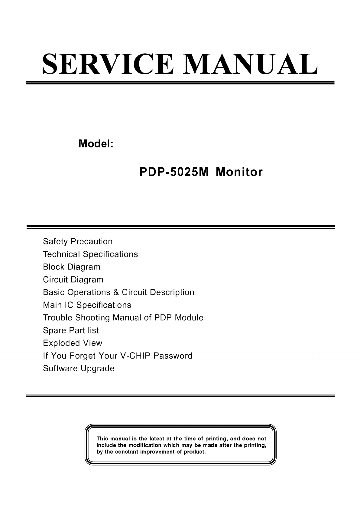
SERVICE MANUAL
Model:
PDP-5025M Monitor
Safety Precaution
Technical Specifications
Block Diagram
Circuit Diagram
Basic Operations & Circuit Description
Main IC Specifications
Trouble Shooting Manual of PDP Module
Spare Part list
Exploded View
If You Forget Your V-CHIP Password
Software Upgrade
This manual is th e la test at the time of printing, and d o e s not
include th e modification which may b e made after th e printing,
by the co n st an t improvement of product.
Page 2

Safety Precaution
CAUTION
RISK OF ELE CTRIC S HOCK
DO NOT OPEN
A
CAUTION: TO REDUCE THE RISK OF
ELECTRIC SHOCK, DO NOT REMOVE COVER
(OR BACK). NO USER-SERVICEABLE PARTS
INSIDE. REFER SERVICING TO QUALIFIED
SERVICE PERSONNEL ONLY.
A
The lightning flash with arrowhead symbol,
within an equilateral triangle, is intended to
alert the user to the presence of uninsulated
“dangerous voltage” within the product’s enclo
sure that m ay be of sufficient magnitude to
constitute a risk of electric shock to persons.
The exclamation point within an equilateral
triangle is intended to alert the user to the
presence of important operating and
maintenance (servicing) instructions in the
literature accompanying the appliance.
PRECAUTIONS DURING
SERVICING
1. In addition to safety, other parts and
assemblies are specified for conformance with
such regulations as those applying to spurious
radiation. These must also be replaced only
with specified replacements.
Examples: RF converters, tuner units, antenna
selection switches, RF cables, noise-blocking
capacitors, noise-blocking filters, etc.
2. Use specified internal W iring. Note especially:
1) Wires covered with PVC tubing
2) Double insulated wires
3) High voltage leads
3. Use specified insulating materials for hazardous
live parts. Note especially:
1) Insulating Tape
2) PVC tubing
3) Spacers (insulating barriers)
4) Insulating sheets for transistors
5) Plastic screws for fixing micro switches
4. When replacing AC primary side components
(transformers, power cords, noise blocking
capacitors, etc.), wrap ends of wires securely
about the terminals before soldering.
5. Make sure that wires do not contact heat
generating parts (heat sinks, oxide metal film
resistors, fusible resistors, etc.)
6. Check if replaced wires do not contact sharply
edged or pointed parts.
7. Make sure that foreign objects (screws, solder
droplets, etc.) do not rem ain inside the set.
MAKE YOUR CONTRIBUTION
TO PROTECT THE
ENVIRONMENT
Used batteries with the ISO symbol
\5<9
for recycling as well as small accumulators
(rechargeable batteries), mini-batteries (cells) and
starter batteries should not be thrown into the
garbage can.
Please leave them at an appropriate depot.
WARNING:
Before servicing this TV receiver, read the
SAFETY INSTRUCTION and PRODUCT
SAFETY NOTICE.
SAFETY INSTRUCTION
The service should not be attempted by anyone
unfamiliar with the necessary instructions on this
apparatus. The following are the necessary
instructions to be observed before servicing.
1. An isolation transformer should be connected in
the power line between the receiver and the
AC line when a service is performed on the
primary of the converter transformer of the set.
2. Comply with all caution and safety related
provided on the back of the cabinet, inside the
cabinet, on the chassis or picture tube.
3. To avoid a shock hazard, always discharge the
picture tube's anode to the chassis ground
before removing the anode cap.
4. Completely discharge the high potential voltage
of the picture tube before handling. The picture
tube is a vacuum and if broken, the glass will
explode.
Page 3

5. When replacing a MAIN PCB in the cabinet,
always be certain that all protective are
installed properly such as control knobs,
adjustment covers or shields, barriers, isolation
resistor networks etc.
6. When servicing is required, observe the original
lead dressing. Extra precaution should be given
to assure correct lead dressing in the high
voltage area.
7. Keep wires away from high voltage or high
tempera ture components.
8. Before returning the set to the customer,
always perform an AC leakage current check
on the exposed m etallic parts of the cabinet,
such as antennas, terminals, screwheads, metal
overlay, control shafts, etc., to be sure the set
is safe to operate without danger of electrical
shock. Plug the AC line cord directly to the
AC outlet (do not use a line isolation
transformer during this check). Use an AC
voltmeter having 5K ohms volt sensitivity or
more in the following manner.
Connect a 1.5K ohm 10 watt resistor paralleled
by a 0.15pF AC type capacitor, between a
good earth ground (water pipe, conductor etc.,)
and the exposed metallic parts, one at a time.
Measure the AC voltage across the combination
of the 1.5K ohm resistor and 0.15 uF
capacitor. Reverse the AC plug at the AC
outlet and repeat the AC voltage measurements
for each exposed metallic part.
The measured voltage must not exceed 0.3V
RMS.
This corresponds to 0.5mA AC. Any value
exceeding this limit constitutes a potential
shock hazard and must be corrected
immediately.
The resistance measurement should be done
between accessible exposed metal parts and
power cord plug prongs with the power switch
"ON". The resistance should be more than
6M ohms.
AC V O L TM E TER
PRODUCT SAFETY NOTICE
Many electrical and mechanical parts in this
apparatus have special safety-related
characteristics.
These characteristics are offer passed
unnoticed by visual spection and the protection
afforded by them cannot necessarily be obtained
by using replacement components rates for a
higher voltage, wattage, etc.
The replacement parts which have these
special safety characteristics are identified by A
marks on the schem atic diagram and on the parts
list.
Before replacing any of these components,
read the parts list in this manual carefully. The
use of substitute replacem ent parts which do not
have the same safety characteristics as specified
in the parts list may create shock, fire, or other
hazards.
9. Must be sure that the ground wire of the AC
inlet is connected with the ground of the
apparatus properly.
Good earth ground
such as the w ater
- p ip e, condu cto r,
etc.
AC Leakage C urrent Check
1500 oh m i, lOwatt
Place this probe
on each exposed
metallic part
Page 4
Technical Specifications
M O D E L : PDP-5025M Monitor
5 0 ” Pla s m a D is p lay
DATE FIRST ISSUED ISSUE
RAISED BY :
RAISED BY CHECKED BY NUMBER OF PAGE
1
------10-------
DATE
R & D DEPARTMENT
COMMERCIAL DEPARTMENT
PRODUCTION DEPARTMENT
Q/A DEPARTMENT
CUSTOMER
SIGNATURE : DATE :
NOTE :
O i l y d oc u m e n t s s t a m p ed ‘Co n tr o ll e d D oc ume nt ” to be u se d f or m a nu f a c t ur e o f pr o d uc ti o n p a rts .
Page 5

CONTINUATION PAGE
Technical Specifications
1. S ta n d a rd T e s t C o n d itio n s
PDP-5025M
NUMBER 2 OF 1 0 PAGES
All tests shall be performed under the following conditions, unless otherwise specified.
1.1 Ambient light
1.2 Viewing distance
1.3 Warm up time
1.4 PDP Panel facing
1.5 Measuring Equipment
1.6 Magnetic field
1.7 Control settings
1.8 Power input
1.9 Ambient temperature
1.10 Display mode
150ux (When measuring IB, the ambient luminance
= 0.1Cd/m2)
50cm in front of PDP
30 minutes
no restricted
PC, Chroma 2225 signal generator (with Chroma digital
additional card) or equivalent, Minolta CA100 photometer
no restricted
Brightness, Contrast, Tint, Color set at Center(50)
100~120Vac
20°C ± 5°C (68°F ± 9°F)
31.5KHz/60Hz (Resolution 1366 x 768)
1.11 Other conditions .
1.11.1 With image sticking protection of PDP module, the luminance will descend
by time on a same still screen and rapidly go down in 5 minutes. When
measuring the color tracking and luminance of a same still screen, be sure t
o accomplish the measurement in one minute to ensure its accuracy.
1.11.2 Due to the structure of PDP, the extra-high-bright same screen should not
hold over 5 minutes for fear of branding on the panel.
Page 6

Technical Specifications
E L E C T R IC A L C H A R A C T E R IS T IC S
2. P o w e r In p u t
PDP-5025M
CONTINUATION PAGE
NUMBER 3 OF 10 PAGES
2.1 Voltage
2.2 Input Current
2.3 Maximum Inrush Current
Test condition
2.4 Frequency
2.5 Power Consumption
Test condition
2.6 Power Factor
2.7 Withstanding voltage
3. D is p la y
3.1 Screen Size
3.2 Aspect Ratio
3.3 Pixel Resolution
3.4 Peak Brightness
3.5 Contrast Ratio (Dark room)
3.6 Viewing Angle
3.7 OSD language
100 ~120VAC
5.0 /2.5A
<30 A (FOR AC110V ONLY)
Measured when switched off for at least 20 mins
50Hz to 60Hz(±3Hz)
450W Typical
full white display with maximum brightness and
contrast
Meets I EC 1000-3-2
1.5kVac or 2.2kVdc for 1 sec
50” Plasma display
16:9
1366x768
1000 cd/m2 (Typical, Panel only)
5000:1 (Ratio, Typical, in a dark room, Panel only)
Over 160°
English, Spanish, French
4. Sig n a l
4.1 AV & Graphic input
4.1.1 Composite signal
4.1.2 Y,C Signal
4.1.3 Component signal
4.1.4 Graphic I/P
4.1.5EDID compatibility
4.1.6 I/P frequency
CVBS
S-Video
Y PbPr1, YPbPr2, HDMI compatible
Analog: D-sub 15pin detachable cable
Digital : HDMII
DDC 1.3
fH: 31.5kHz to 60kHz/fV: 56.25Hz to 75Hz (1024X768
recommended)
Page 7

Technical Specifications
PDP-5025M
CONTINUATION PAGE
NUMBER 4 OF 1 0 PAGES
4.2 Audio input
4.3 Audio output
5. E n v iro n m e n t
5.1 Operating environment
5.1.1 Temperature :
5.1.2 Relative humidity:
5.2 Storage and Transport
5.2.1 Temperature :
5.2.2 Relative humidity:
VGA (D-Sub 15 pin Type) *1
D-Sub 9 Pin (RS-232 Input) * 1
HDMI (Ver. 1.1) connector * 1
S-Video (Mini Din 4 Pin) * 1
Video (RCA Type) * 1
YpbPr1/YpbPr2 * 1
Stereo/Audio * 6
Audio (L+R) * 1 Video (RCA Type) * 1 SPDIF (Optical) * 1
PIP/POP/PBP, Picture size, Picture Still, Sound mode,Last
memory, Timer, MTS
5° to 33°C
20% to 85%(non-condensing)
-20°C to 60°C(-4° to 140°F)
5% to 95%
6. P an e l C h a r a c te r is t ic s
6.1 Type :
6.2 Size :
6.3 Aspect ratio
6.4 Viewing angle
6.5 Resolution
6.6 Weight
6.7 Color
6.8 Contrast
6.9 Peak brightness :
6.10 Color Coordinate Uniformity :
Test Pattern :
S50HW-XD03
50”,1106.5mm(W)X622.1mm(H)
16:9
Over 160°
1366X768
22.0kg ±0.5 kg (Net)
16.7 millions of colors (R/G/B each 256 scales)
Average 60:1 (In a bright room with 150Lux at center)
Typical 5000:1 (In a dark room 1/100 White Window
pattern at center).
Typical 1000cd/m2 (1/25 White Window)
Contrast; Brightness and Color control at normal
setting
Full white pattern
Average of point A,B,C,D and E +/- 0.01
Page 8

Technical Specifications
PDP-5025M
CONTINUATION PAGE
NUMBER 5 OF 10 PAGES
6.11 Color temperature
6.12 Cell Defect Specifications
Subject to Panel supplier specification as appends.
7. F ro n t P a n e l C o n tro l B u tto n
7.1 SET Up / Down Button
Volume Left/Right Butt
Menu Button
Source Select Button
Contrast at center (50); Brightness center (50);
Color temperature set at Natural
x=0.285±0.02
y=0.290±0.02
Push the key to select Item up or down.
When selecting the item on OSD menu.
Push the key to increase the volume left or right.
When selecting the adjusting item on OSD menu
increase or decrease the data-bar.
Enter to the OSD menu.
Press this button and use up/down button to sellect
the signal sources. AV, S-Video, YPbPr1,YPbPr2
VGA or HDMI.
7.2 Stand by Button
Switch on main power, or switch off to enter power
Saving modes.
7.3 Main Power Switch
8. O S D F u n c tio n
Turn on or off the unit.
8.1 Picture : State (Normal,Dark,Bright,User); Display (Bright,contrast,Color,Hue)
Temp (warm,Cool,Normal,User);
Position (H-posit,V-posit,Phase,H-size,Auto Adjust)
8.2 Sound : Setup (Mode,AVC,Volume,Balance);
Equalizer (120HZ,500HZ,1.5KHZ,5KHZ,10KHZ)
BBE Setup (Gain,Treble,Bass)
8.3 OSD : Size (Panorama,16:9,Normal,Anamorphic,Letter Box,TV Mode)
OSD Set (Language,OSD Position,Time Out)
Option (Burn Protect, Version)
V-Chip , C/C
8.4 Layout : Layout (Full Screen,PIP,Split Screen,Grid,POP 3,POP 12)
PIP Set (Sub Win Source,Sub Win Size,PIP Size.PIP Position)
8.5 Time : Sleep (30Min,60Min,90Min,120Min,180Min)
Wake Up (Time Edit,Volume,TV Mode,Channel)
Time Set
Page 9

Technical Specifications
9. A g e n c y A p p ro v a ls
Safety UL/FCC/cUL
Emissions FCC class B
10. R e liab ilit y
PDP-5025M
CONTINUATION PAGE
NUMBER 6 OF 10 PAGES
11.1 MTBF
11. A c c e s s o rie s
20,000 hours(Use moving picture signal at 25°C ambient)
User manual x1, Remote control x1, Stand x1,
Battery x 2, Accessories box x 1, AC Cable x1
Page 10
Technical Specifications
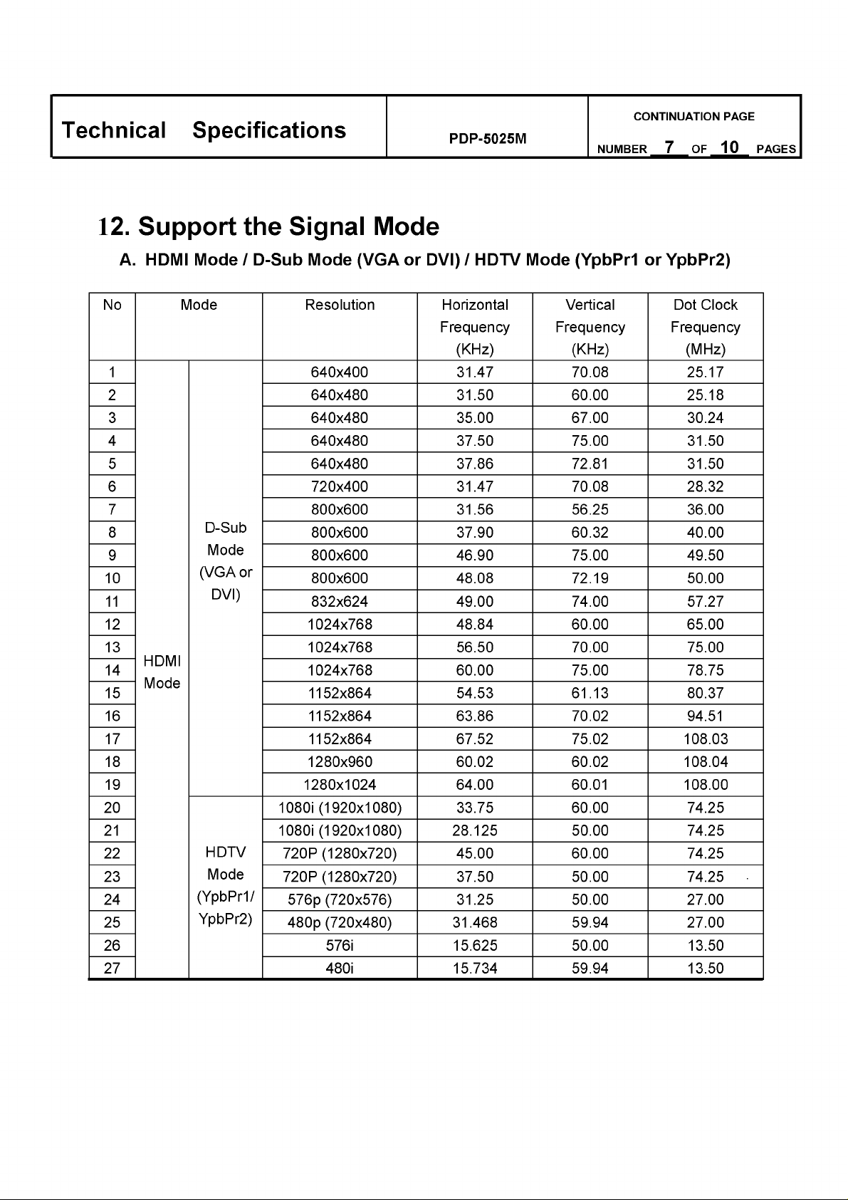
12. Support the Signal Mode
A. HDMI Mode / D-Sub Mode (VGA or DVI) / HDTV Mode (YpbPrl or YpbPr2)
PDP-5025M
CONTINUATION PAGE
NUMBER 7 OF 10 PAGES
No Mode Resolution Horizontal
Frequency
(KHz)
1 640x400 31.47 70.08 25.17
2 640x480 31.50 60.00 25.18
3 640x480 35.00 67.00 30.24
4 640x480 37.50 75.00 31.50
5 640x480 37.86 72.81 31.50
6 720x400 31.47 70.08 28.32
7 800x600 31.56 56.25 36.00
8
9
10
11
12 1024x768 48.84 60.00 65.00
13
HDMI
14 1024x768 60.00 75.00 78.75
Mode
15
16 1152x864 63.86 70.02 94.51
17 1152x864 67.52 75.02 108.03
18 1280x960 60.02 60.02 108.04
19 1280x1024 64.00 60.01 108.00
20 1080i (1920x1080) 33.75 60.00 74.25
21 1080i (1920x1080) 28.125 50.00 74.25
22
23
24
25
26 576i 15.625 50.00 13.50
27 480i 15.734 59.94 13.50
D-Sub
Mode
(VGA or
DVI)
HDTV
Mode
(YpbPr1/
YpbPr2)
800x600 37.90 60.32 40.00
800x600 46.90 75.00 49.50
800x600 48.08 72.19 50.00
832x624 49.00 74.00 57.27
1024x768 56.50 70.00 75.00
1152x864 54.53 61.13 80.37
720P (1280x720) 45.00 60.00 74.25
720P (1280x720) 37.50 50.00 74.25
576p (720x576) 31.25 50.00 27.00
480p (720x480) 31.468 59.94 27.00
Vertical
Frequency
(KHz)
Dot Clock
Frequency
(MHz)
Page 11

Technical Specifications
4.4 Remote Control
1 POWER(cb): Press this button to turn off to
standby and turn on from standby.
2 MUTE(jc): Press this button to quiet the sound
system. Press again to reactivate the
sound system.
3 P.STILL: Press this button to hold on the
screen. Press again to normal.
4 P.SIZE: When the input source is YPbPr 1,
YPbPr 2, VGA or HDMI, press this button,
the picture will change according to Fill All,
Force 4:3, Letter Box, Wide or Anamorphic.
When the input source is AV or S-Video, press
this button, the picture will change according to
Fill All, 4:3, Letter Box, Wide or Anamorphic.
5 S.SELE: Press this button to select the sound
output from Main Window or Sub Window.
6 P.MODE : Press the button to select different
picture effect.
7 TIME: Press this button to pop up the "Clock
Set” menu.
8 SLEEP: Press this button to select the sleep
time.
9 INFO: Press the button to display the
source information.
10 AUTO: The Display automatically adjusts the
phase, vertical / horizontal position when
pressing this button in VGA mode.
11 LAYOUT: Press this button to pop up Layout
menu.
12 C/C: Press this button to enter the Closed
Caption Function. (Only for AV or S-Video)
13 V-CHIP: Press this button to enter the V-Chip
Function. (Only for AV or S-Video)
14 Number buttons: Use these buttons to enter
the password.
PDP-5025M
CONTINUATION PAGE
NUMBER 8 OF 10 PAGES
2
5
6
9
10
12
13
14
18
19
22
23
25
(Continued on next page)
Page 12

Technical Specifications
PDP-5025M
CONTINUATION PAGE
NUMBER 9 OF 10 PAGES
15 SWAP: Press this button to switch the Main
window or Sub window pictures in PIP and
Split Screen.
16 F.WHITE: Press this button to show a full
white picture.
17 PIP POS. : Press the button to select different
Image Position in PIP Mode.
18 PIP SIZE : Press the button to select different
Image Size in PIP Mode.
19 SPEAKER: Press this button to pop up the
"Speaker” menu, use the ^ / ► butt°n t° select
"Internal” or "External”.
20 SOUND: Press the button to select different
sound effect.
21 W.SELE: Press this button to select the Main
Window or Sub Window.
22 SOURCE: Press this button and use ▲ / T
button to select the signal sources. AV, S-Video,
YPbPr 1, YPbPr 2, VGA or HDMI.
23 PIP: Press this button to change different
Picture Mode.
24 MENU: Press this button to pop up the OSD
Menu and press it again to exit the OSD Menu.
25 OK : Press to enter or confirm.
26 -4 / ► : They are used as -4 / ► buttons in the
OSD Menu screen and they can be used for
the adjustment of volume when the OSD Menu
is not shown on the screen.
▲ / ▼ : They are used as ▲ / ▼ buttons in the
OSD Menu screen.
They also can be used for the selection of the
program when the OSD Menu is not shown on
the screen, but only for the Model with Tuner.
2
5
6
9
10
12
13
14
18
19
22
23
25
Page 13

Technical Specifications
P H Y S IC A L C H A R A C T E R IS T IC S
14. P o w e r C o rd
PDP-5025M
CONTINUATION PAGE
NUMBER 1 0 OF 1 0 PAGES
Length
Type
15. C a b in e t
15.1 Color
15.2 Weight
Net weight
Gross weight
15.3 Dimensions
Width
Height
Depth
1.8m nominal
optional
black colour as defined by colour plaque reference number
51kg
74kg
(W/O stand&handles)
1227.8mm
739.8mm
100.5mm
Page 14

Block Diagram
Product Specification of PDP Module
LVDS Input
Control Signal
(Serial Interface)
APL Data
Vs(180V~190V)
Va(55V~65V)
Vcc(+5V)
Display data, Driver timing
Color Plasma Display Panel
1366 X 768 pixels
Address Driver
^ Applied Voltage level is specified at the time when Full-White pattern is displayed on the panel.
Page 15

Block Diagram MAIN / AUDIO BOARD
Page 16
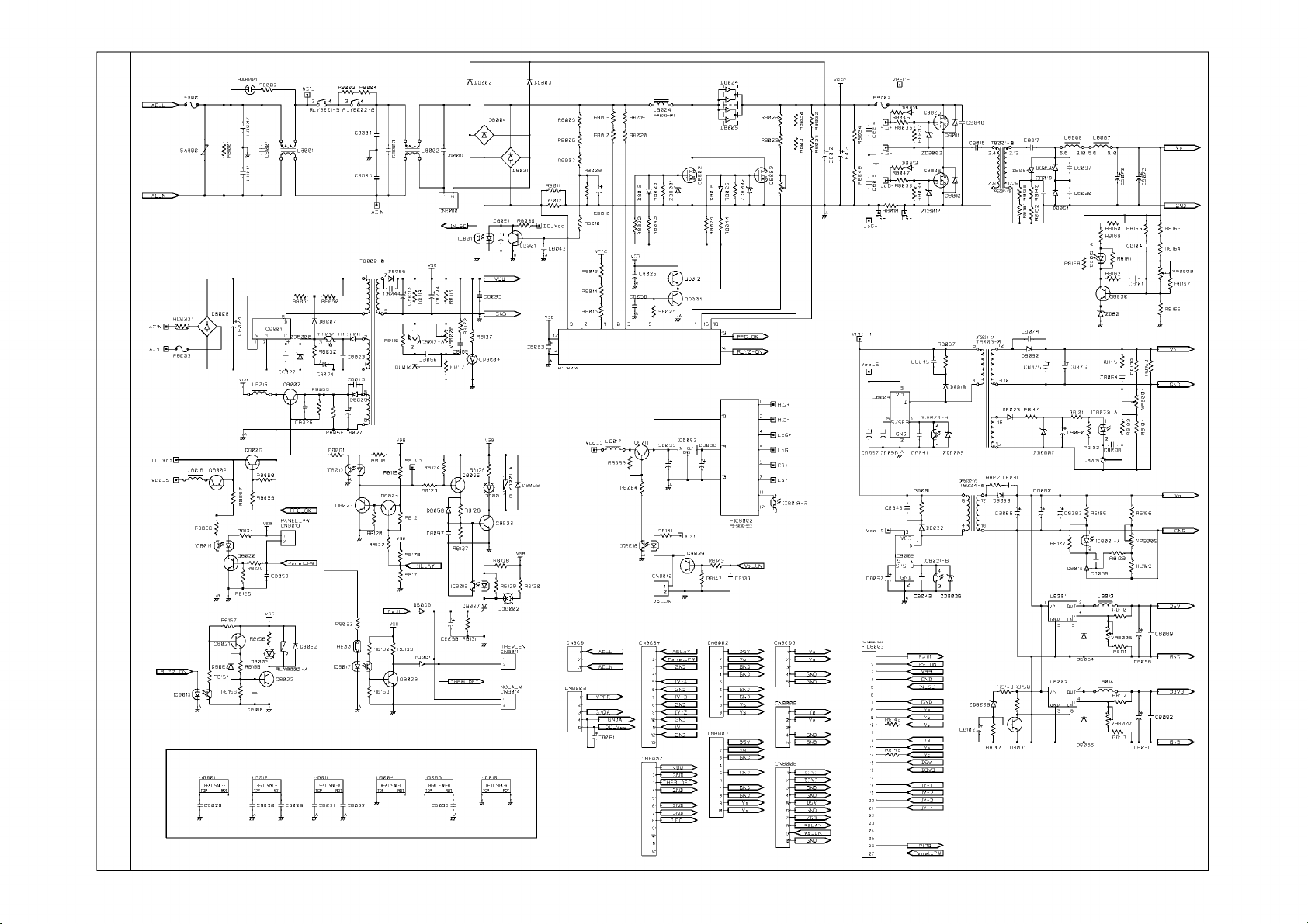
Circuit Diagram
- Power supply board of Audio Amplifier,
- Main (Video) board
- Audio/Tuner board
- Keypad board
- Remote control receiver board
- Remote control board
Page 17

MPT012A
Page 18
Page 19

PT.T.1 8V OVDD3 3V#
Using digital interface:
DVdd (1.8V) (DVdd+CVdd) 130mA 234mW
PVd (1.8V) (PVd+ALVdd) 30mA 54mW
D D
B B
DDC SCL5 D S DDC SCL3
R919^ ^ J q901
HSOUT
SOGOUT
VSOUT/AO
FIELD
DCLK
DDC5V 1
DDC SDA5
92
93
94
95
96
97
98
99
2 ADCB7
3 ADCB6
4 ADCB5
7 ADCB2
BO
88
DE
87
86
85
84
89
Ö R925
R920 °
D S
R924
ADC DCLK
Q902
R916 -
R929
l
R921
—
R922
Vd (3.3V) (Avdd+TVdd) 80mA 264mW
Vdd (3.3V) (Ovdd) 10-120mA, 30mA typical
99mW
Using analog interface:
TVDD3.3V
DVdd 60mA 108mW
PVd 20mA 36mW
DDC SDA3
Vd 270mA 891mW
C
MCLKIN
MCLKOUT
SCLK
LRCLK
1250
1251
1252
1253
A A
Title
9-HDMI-R
SizeBNumber Revision
Date: 14-O ct-2005 Sheet of
File:
F:\4228\4228 temp ddb\4228 Temp.DDB Drawn By:
Page 20

Page 21

Page 22

Page 23

Page 24

■ |c13Ö4 |c13Ö5 C1306 C1307 C1308 C130
T T TTTTT
2 L1304 VT5
4 II |+ IC1331 |C1330 |C1329 |C132
— i c t-T
f t o i I I I J
D
13 Ic1314 C1315 C1322 C1321 C1320 C1319 C1318 C1317 ^C131
TTTTTTTTT
3 C1334 C1335 C1336 C1337 C1338 Cc1339 Cu340 'c1341 Cm 2 Cc134
A A
T
13-SCALER
II ___T TTT
Page 25

31RAMA0 40
31RAMA1 38
31RAMA2 36
31RAMA3 34
31RAMA4 33
31RAMA5 35
31RAMA6 37
31RAMA7 39
D D
5LOCK
31RAMA8 41
31RAMA9 43
31RAMA10 42
31RAMA11 45
31RAMA1246
31RAMA13 44
204
MA0
MD
MA1
MD
MA2
MD
MA3
MD
MA4
MD
MA5
MD
MA6
MA7
MA8
MA9
MA10
MA11
MA12
MA13
- MCLK MRAS
MCAS
MWE
U1201C
V33SW
MD9
MD8
MD7
MD6
MD5
MD4
67
6947
48 R121
49 R1217
50
31RAMD15
31RAMD14
31RAMD13
RAMD12
RAMD11
RAMD10
WE
17 31CASn
CAS
MM
'i iyiyo
¿QQ S
DQ10
DQ11
DQ12
DQ13
DQ14
DQ15
RAS
DQ0
DQ1
DQ2
DQ3
DQ4
DQ5
DQ6
DQ7
42
DQ8
44
DQ9
45
47
48
50
53
37
CKE
RAMD3
RAMD6
RAMD9
38
31RAMA0 23
31RAMA1 24
Cl242 C1205 C1206 C1207 C1208 C12C
T TTTT^
ADR:0x64
B B
A A
- VSS0
- VSS1
104
VSS2
134
VSS3
- PVSS0
- PVSS1
53
PVSS2
79
PVSS3
91
PVSS4
122
PVSS5
147
PVSS6
78
76
123
ADDVSS PW1231P0WER .
29
- ADAVSS ADAVDD
32
- ADGVSS ADGVDD
- AVS33B AVD33B
- AVS33G AVD33G
- AVS33R AVD33R
4
- AVS33SVM AVD33SVM
VDD0
VDD1
VDD2
VDD3
PVDD0
PVDD1
PVDD2
PVDD3
PVDD4
PVDD5
PVDD6
70
V25SW
_T
V33SW1
146
AV25p1
----
AV25p2
AND GROUND
28 “ I AV25a
â=i_
22
AV331
_ T
V33SW
T
__
C1210 C1212 C1213 C1214 C1215 C1216 C121
TTTTTT
V33SW1 V25SW AV25P1 V25SW
C1227 C1228 C1229 C1230 C1231 C1232 C123
C1247 C1246
‘TTTTTTT
X F I | 221 C 122
’I T T T T
C1234 C1235 C1:
' I X -
AV25A V33SW
C1250
C1237 C1238 C1239 C 124
'TTTT
C1224 C1:
X
31RAMA2 25
31RAMA3 26
31RAMA4 29
31RAMA5 30
31RAMA6 31
31RAMA7 32
31RAMA8 33
31RAMA9 34
31RAMA10 22
31RAMA11 35
31RAMA12 20
31RAMA13 21
B
Date: 14-0ct-2005
File: F:\4228V4228 tempddb\4228 Temp.DDB Drawn B
U1203
A0
A1
A2
A3
A4
A5
A6
A7
A8
A9
A10
A11
12-DEINTERLACE
Number Revisi
C
Page 26

Page 27

I. * T
RSTINn 2
TLCCT 3
U403
SENCE Vdd
RESin
RESET
CT
____
RESET
CONTROL
GND
ADR:0xA0/MEMORY
ADR:0xD0/ COMPANION
R422
RESETn
R406
D
A A
T
4-FLASH
Numb
A3
F:\4228\4228 temp ddb\4228 Temp.DDBDrawn By:
et of
Page 28

4
For sumsung panel standard LVD S jack
TX0
D D
TX1
TX2
12
CK
16
TX3
20 501 502
C C
NC
For sumsung panel
DRE0
DRE1
DRE2
DRE3
DRE4
DRE5
DRE6
DRE7
B B
DGE0
DGE1
DGE2
DGE3
DGE4
DGE5
DGE6
DGE7
DB E0
DBE1
DB E2
DBE3
DB E4
DBE5
DB E6
DB E7
A A
DR E[7..0t»
DG E[7 ..0H
DB Ef7..0l>
DHS
DVS
DEN
LVD33
T
_
DHS 27
DVS 28
< DEN 30
>
L501
For LG panel
DRE2 51
DRE3 52
DRE4 54
DRE5 55
DRE6 56
DRE7
DRE0
DRE1 2
x
DGE2 4
S
DGE3 6
s
DGE4 7
s
DGE5 11
s
DGE6 12
s
DGE7 14
s
DGE0 8
\
DGE1 10
DBE2 15
s
DBE3 19
s
DBE4 20
s
DBE5 22
s
DBE6 23
s
DBE7 24
s
DBE0 16
\
DBE1 18
—j —C520 — — C522 —j— C
LVD_V
—I— C
JÜ
-C523 —1— C525
"L
RS
I
d
s
31
50
I - 0
K
V
TxIN0
TxIN1
TxIN2 TxOUT0+
TxIN3 TxOUT1-
TxIN4 TxOUT1+
TxIN6 TxOUT2-
TxIN27 TxOUT2+
TxIN5 TxOUT3-
TxIN7 TxOUT3+
TxIN8 TxCLKOUT-
TxIN9 TxCLKOUT+
TxIN12
TxIN13
TxIN14
TxIN10 PW R DWN
TxIN11
TxIN15
TxIN19
TxIN20 PLL GND
TxIN21 PLL GND
TxIN22
TxIN16
TxIN17 LVDS GND
TxIN24 LVDS GND
TxIN25 LVDS GND
TxIN26
TxIN23
U501
/ DS90C 385AMTD
L504
i
_
R504
TX0- 1 2
TX0+ 3
TX1- 5 6 P SCLK
TX1+ 7
TX2- 9
TX2+ 11
CK- 13 4 P SCLK#
CK+ 15
TX3+ 19
C
C
C
C
C
C
V
VCC
V
V
S
L
D
PL TxOUT0-
V
L
R FB
GND
GND
GND
GND
O
4
8
P SDA TA# P SLE
P SLE#
P DISPEN#TX3- 17 P DISPEN
20
— SCL S3V
— SD A S 3V )
For LG panel standard LVD S jack
TX0-
TX1-
TX2-
CK-
TX3- 11
1
10
12
13
14
PDPGO
I.
p dispen# 27
p sdata#
p sclk#
29
I sle#
30
31
NC SGND
Title
Size
Number Revision
A4
Date: 14-Oct-2005 Sheet of
File: F:\4228\4228 temp ddb\4228 Temp.DDI5 Drawn By: ANDY
rY Y TV.
C527
R513
______
l _ L 505o
—I— C528
I
L506
IRQ
X
L503
YTYYV
- I -
r
INPUT OUTPUT
O
5-LVDS&TMDS
Formosa panel CPUGO
---------(r e L a y o n # I
P SDATA
Formosa panel PDPGO
---------( V s on # I
P SCLK
TAB
P SDATA
P SLE
P DISPEN
00
Page 29

Page 30

Page 31

Audio.Board.BH(M-CH).05.06.14.sch-1 - Tue Aug 16 22:15:14 2005
Page 32

DUBHE OSD Ver1.1 NAKS.sch-1 - Mon Oct 1B 11:47:11 2004
Page 33

R702
56K
- w -
REMOTE PCB
VD701
IN4148
X°“ l
O K51
yo-<>
X°~l
OK47
<?K48
^O—11
9K44
✓o-hI
^K43
✓O—11
QK 36 gK35
X°n
£ K 5 0
^O-i i
£K46
^Ohi
^K42
✓ O -o
£K38
^ O - o
gK34
✓ ° i
OK49
/'CHI
OK45
fO-ii
Q K41
^O—< I
OK37
^CHI
gK33
✓ ° 1
OK32
QK 28
p/ O—< I
OK24
yo-<>
gK20
£k16
^ O - H
gK12
✓ O h >
gK8
^ C H I
g K 4
0K31
yo->>
gK27
fO-o
~ K19
^ O H I
~K15
ycxi
~*K11
yen i
>K7
^ O -o
g K3
^/O-i /'O-i
OK3 0 OK29
gK26
gK25
✓ C H »
^/Ohi
gK22
gK21
^ C H i
gK 18
£ K 1 7
yo~> >
g K13
^CH I
gK10
✓ O h »
£ K 6
gK 5
✓CH I
^/Ohi
_gK2
g K1
»
- 2 ±
JÄ.
J£.
JZ.
ja.
ja .
¿a.
21
22.
21
LL
N701
PT2222
_ rv
X L .
€70 2
150pF
□
G701 'i ^ n ,
455KHZ
a 150pF
B701
BT701
3V
H'l
C701
^7U /10V
+ 0 —
R701?701<
A°wf
V701
80 50
Page 34

REMOTE CONTROL CODE ASSIGNMENT
KEY NO. KEY NAME DATA CODE KEY NO. KEY NAME DATA CODE
K1 POWER 00 K33 dumb 40
K2
K3
K4
K5 P.MODE 04 K37
K6
K7 5 06 K39 nil 46
K8
K9
K10 7 09 K42 PREV 49
K11 8 OA K43 P.STILL 4A
K12 9 OB K44 SOUND 4B
K13 MTS OC K45 SLEEP 4C
K14 nil OD K46
K15
K16
K17
K18
K19
K20
K21 MENU 14 K53 nil 54
K22
K23
K24
K25 0 18 K57 nil 58
K26
K27
K28 EXIT 1B K60 nil 5B
K29 PIP 1C K61 nil
K30
K31
K32 PIP CH+ 1F K64
1
2 02 K35
3
4
6
nil
S.SELE
OK
CH.+
VOL.+
VOL.-
CH .- 13 K52 nil 53
Source
nil
P.SIZE
F.White
PIP Source
SWAP
PIP CH-
01 K34
03 K36 dumb 43
05 K38
07 K40 nil 47
08 K41 100 48
OE K47 Picture 4E
OF K48 CH Erase 4F
10 K49
11 K50 C /C 51
12 K51
15 K54 nil 55
16 K55 nil 56
17 K56
19 K58
1A K59 nil 5A
1D K62 nil 5D
1E K63 nil 5E
dumb
dumb
MUTE
INFO
TIME
CH Save
V-CHIP
nil
nil
nil
41
42
44
45
4D
50
52
57
59
5C
5F
CUSTOM CODE: 20DD
0025.sch-1 - Mon May 16 09:25:50 2005
FOR NTSC
Page 35

Basic Operations & Circuit Description
MODULE
There are 1 pc. panel and 12 pc.s PCB including 2 pc.s Y/Z Sustainer board, 2 pc.s Y Drive
board, 6 pc.s X Extension boards, 1 pc. Control (Signal Input) and 1 pc. Power
board in the Module.
SET
There are 6 pc.s PCBs including 1 pc. AUX. PSU Board, 1 pc. Keypad board, 1 pc.
Remote Control Receiver board, 1 pc. L/R Speakers and 1 pc. Main (Video) board in the SET.
Page 36

X-extension Top
L/C/R
Control
Board Assy
Power supple
Page 37

PCB function
1. Power:
(1). Input voltage: AC 100V~120V, 45Hz~60Hz.
Input range: AC 90V(Min)~265V(Max) auto regulation.
(2). To provide power for PCBs.
2. Main (Video InterFace) board: To converter TV signals, S signals, AV signals, Y Pb/
Cb Pr/Cr signals, DVI signals and D-SUB signals to digital ones and to transmit to
Control board.
3. Control board: Dealing with the digital signal for output to panel.
4. Y-Sustainer / Z-Sustainer board:
(1). Receiving the signals from Control and high voltage supply.
(2). Output scanning waveform for Module.
5. Y-Drive board: Receive signal from Y sustainer, output horizontal scanning wave
form to the panel.
6. X extension board (6pcs): Output addressing signals.
7. Tuner/Audio Board: Process and Amplifying the audio signal to speakers and
convert TV RF signal to video/audio signal and send to Main board.
Page 38

PCB failure analysis
1. CONTROL
2. MAIN (video) :
3. POWER
4. Z - Sustainer
5. Y - Sustainer
6. X - Extension : Abormal vertical noise on screen.
7. Audio Board or AUX PSU: a. No voice. (Make sure Mute/OFF)
: a. Abnormal noise on screen. b. No picture.
a. Lacking color, Bad color scale.
b. No voice.
c. No picture but with signals output, OSD and back light.
d. Abnormal noise on screen.
: No picture, no power output.
:a. No picture.
b. Color not enough.
c. Flash on screen.
: Darker picture with signals.
b. Noise.
Page 39

Basic operation of Plasma Display
1. A fter turning on pow er switch, power board sends 5Vst-by Volt to Micro Processor
2. The m icro Processor m em orize the last state of Power, W hen the last state of
pow er is on or receive power on signal from local Key or Rem ote control, Micro
Processor will send on control signal to power. Then Power sends (5Vsc, 9Vsc,
24V and RLYON, Vs ON) to PCBs w orking. This time VIF will send signals to
display Image, O SD on the panel and start to search available signal sources.
If the audio signals input, them will be amplified by Audio AMP and transm itted to
Speakers.
3. If som e abnorm al signals are detected (for example: over volts, over current, over
tem perature and under volts), the system will be shut down by Power off.
Page 40

Main IC S p e c ifica tion s
- PW181 Image Processor, Scaler
- PW1231 Digital Video Signal Processor
- VPC 323XD Comb-filter Video Processor
- Z86229 NTSC Line 21 CCD decorder
- MSP34x0G Multistandard Sound Processor
-AD9880 Analog/HDMI Dual Display Interface
-PI5V330 Wideband/Video Quad 2-Channel MUX/DEMUX
-SM5304AV Video Buffer with Built-in Analog LPF
-TDA2616 2 X 12 W hi-fi audio power amplifier with mute
-SAA5360 Multi page intelligent teletext decoder
-AT24C32 Z-Wire Serial EEPROM
-HT48R06A-1 8-Bit Cost-Effective I/O Type MCU
Page 41

PW181
Product Specification
General Description
The PW181 ImageProcessor is a highly integrated
“system-on-a-chip” that interfaces computer graphics and
video inputs in virtually any format to a fixed-frequency flat
panel display.
Computer and video images from NTSC/PAL to WUXGA
at virtually any refresh rate can be resized to fit on a fixed-
frequency target display device with any resolution up to
WUXGA. Video data from 4:3 aspect ratio NTSC or PAL
and 16:9 aspect ratio HDTV or SDTV is supported. Multi
region, nonlinear scaling allows these inputs to be resized
optimally for the native resolution of the display.
Advanced scaling techniques are supported, such as
format conversion using multiple programmable regions.
Three independent image scalers coupled with frame
locking circuitry and dual programmable color lookup
tables create sharp images in multiple windows, without
user intervention.
Embedded SDRAM frame buffers and memory controllers
perform frame rate conversion and enhanced video
processing completely on-chip. A separate memory is
dedicated to storage of on-screen display images and
CPU general purpose use.
Advanced video processing techniques are supported
using the internal frame buffer, including motion adaptive,
temporal deinterlacing with film mode detection. When
used in combination with the new third-generation scaler,
this advanced video processing technology delivers the
highest quality video for advanced displays.
Both input ports support integrated DVI 1.0 content
protection using standard DVI receivers.
A new advanced OSD Generator with more colors and
larger sizes supports more demanding OSD applications,
such as on-screen programming guides. When coupled
with the new, faster, integrated microprocessor, this OSD
Generator supports advanced OSD animation techniques.
Video
TV
Signal
TV
Signal
Input
TV Tuner
Com puter
Com puter
j TV Tuner j
Video
Input
Video
Decoder
ADC/
TMDS
ADC/
TMDS
r 1
Video
Decoder
PW181 System Block Diagram
Crystal
~ r
PW181
ROM
Features
• Third-generation, two-dimensional filtering techniques
• Third-generation, advanced scaling techniques
• Second-generation Automatic Image Optim ization
• Fram e rate conversion
• Video processing
• On-Screen Display (OSD)
• On-chip microprocessor
• JTAG debugger and boundary scan
• Picture-in-picture (PIP)
• M ulti-region, non-linear scaling
• Hardware 2-wire serial bus support
Applications
• M ultimedia Displays
• Plasma Displays
• Digital Television
Device Application Package
PW181-10V Up to XGA Displays
PW181-20V Up to UXGA Displays
352 PBGA
Dis p lay
Programmable features include the user interface, custom
start-up screen, all automatic imaging features, and
special screen effects.
p ix e lw o r k s
8100 SW Nyberg Road
Tualatin, OR 97062 USA
Telephone: 503.454.1750
FAX: 503.612.0848
www.pixelworks.com PRELIMINARY I CONFIDENTIAL
Page 42

AN ALO G 110 MSPS/140 MSPS Analog Interface
►
FEATURES
140 MSPS Maximum Conversion Rate
300 MHz Analog Bandwidth
0.5 V to 1.0 V Analog Input Range
500 ps p-p PLL Clock Jitter at 110 MSPS
3.3 V Power Supply
Full Sync Processing
Sync Detect for “Hot Plugging”
Midscale Clamping
Power-Down Mode
Low Power: 500 mW Typical
4:2:2 Output Format Mode
APPLICATIONS
RGB Graphics Processing
LCD Monitors and Projectors
Plasma Display Panels
Scan Converters
Microdisplays
Digital TV
DEVIC ES for Flat Panel Displays
AD9883A
FUNCTIO N A L BLOCK DIAG R A M
GENERAL DESCRIPTION
The AD9883A is a complete 8-bit, 140 MSPS monolithic analog
interface optimized for capturing RG B graphics signals from
personal computers and workstations. Its 140 M SPS encode
rate capability and full power analog bandwidth of 300 MHz
supports resolutions up to SXGA (1280 x 1024 at 75 Hz).
The AD 9883A includes a 140 MHz triple ADC with internal
1.25 V reference, a PLL, and programmable gain, offset, and
clamp control. The user provides only a 3.3 V power supply,
analog input, and Hsync and CO A ST signals. Three-state
CMOS outputs may be powered from 2.5 V to 3.3 V.
The AD9883A’s on-chip PL L generates a pixel clock from the
Hsync input. Pixel clock output frequencies range from 12 MHz to
140 MHz. PLL clock jitter is 500 ps p-p typical at 140 MSPS.
When the CO AST signal is presented, the PLL maintains its
output frequency in the absence of Hsync. A sampling phase
adjustment is provided. Data, Hsync, and clock output phase
relationships are maintained. The AD9883A also offers full sync
processing for composite sync and sync-on-green applications.
A clamp signal is generated internally or may be provided by
the user through the CLAMP input pin. This interface is fully
programmable via a 2-wire serial interface.
Fabricated in an advanced CM OS process, the AD9883A is
provided in a space-saving 80-lead LQFP surface-mount plastic
package and is specified over the 0°C to 70°C temperature range.
REV. A
Information furnished by Analog Devices is believed to be accurate and
reliable. However, no responsibility is assumed by Analog Devices for its
use, nor for any infringements of patents or other rights of third parties that
may result from its use. No license is granted by implication or otherwise
under any patent or patent rights of Analog Devices.
One Technology Way, P.O. Box 9106, Norwood, MA 02062-9106, U.S.A.
Tel:
Fax:
Page 43

PW1231A
Product Specification
General
The PW1231A is a high-quality, digital video signal
processor that incorporates Pixelworks' patented
deinterlacing, scaling, and video enhancement
algorithms. The PW1231A accepts industry-standard
video formats and resolutions, and converts the input into
many desired output formats.The highly efficient video
algorithms result in excellent quality video.
The PW1231A combines many functions into a single
device, including a memory controller, auto-configuration,
and others. This high level of integration enables simple,
flexible, cost-effective solutions that require fewer
components.
Crystal
Video
PW1231A
System Block Diagram
Video
Decoder
PW1231A
PW1231AL
SD RAM
Digital
Output
Features
• Built-In Memory Controller
• Motion-Adaptive Deinterlace Processor
• Intelligent Edge Deinterlacing
• Digital Color/Luminance Transient Improvement (DCTI/DLTI)
• Interlaced Video Input Options, including NTSC and PAL
• Independent horizontal and vertical scaling
• Copy Protection
• Two-Wire Serial Interface
Applications:
For use with Digital Displays
• Flat-Panel (LCD, DLP) TVs
• Rear Projection TVs
• Plasma Displays
• LCD Multimedia Monitors
• Multimedia Projectors
Device Application Package
PW1231A
PW1231AL
NOTE: “ L” denotes lead (Pb) free
Up to XGA 160-pin PQF
p ix e lw o r k s
8100 SW Nyberg Road
Tualatin, OR 97062 USA P/N 001-0097-00 Rev B
Telephone: 503.612.6700 J uly 2003
www^xelwoi^s.com PRELIMINARY CONFIDENTIAL
Page 44

ANALOG
DEVICES Analog/HDMI Dual Display Interface
□
Preliminary Datasheet
FEATURES
Analog/HDMI Dual Interface
Supports High-Bandwidth Digital Content Protection
RGB to YCbCr two-way color conversion
Automated clamping level adjustment
1.8/3.3V Power Supply
100-pin LQFP Pb-Free Package
RGB and YCbCr Output Formats
Analog Interface
8-bit Triple Analog to Digital Converters
150 M SPS Maximum Conversion Rate
Macrovision Detection
2:1 Input Mux
Full Sync Processing
Sync Detect for “Hot Plugging”
Mid-Scale Clamping
Digital Video Interface
HDMI 1.0, DVI 1.0
150 MHz HDMI Receiver
Supports High-Bandwidth Digital Content Protection
(HDCP 1.1)
Digital Audio Interface
HDMI 1.0 compatible audio interface
S/PDIF (IEC90658 compatible) digital audio output
Multi-channel I2S audio output (up to 8 channels)
_____
FUNCTIONAL BL O C K D IAGRA M
3/26/2004 AD9880
APPLICATIONS
Advanced TV
HDTV
Projectors
LCD Monitor
GENERAL DESCRIPTION
The AD9880 offers designers the flexibility o f an analog interface
and High-Definition Multimedia Interface (HDMI) receiver
integrated on a single chip. Also included is support for High
bandwidth Digital Content Protection (HDCP).
Analog Interface
The AD9880 is a complete 8-bit 150 MSPS monolithic analog
interface optimized for capturing Component Video (YPbPr) and
RGB graphics signals. Its 150 MSPS encode rate capability and
full power analog bandwidth of 300 MHz supports all HDTV
formats (up to 1080p) and FPD resolutions up to SXG A (1280 x
1024 at 75 Hz).
The analog interface includes a 150 MHz triple ADC with
internal 1.25 V reference, a Phase Locked Loop (PLL), and
programmable gain, offset, and clamp control. The user provides
only 1.8V and 3.3V power supply, analog input, and Hsync.
Three-state CMOS outputs may be powered from 1.8V to 3.3V.
The A D9880’s on-chip PLL generates a pixel clock from Hsync.
Pixel clock output frequencies range from 12 MHz to 150 MHz.
AD9880 Preliminary Technical Information
Informa tion furn is he d by An alo g Devices is believed to be accura te and re liable .
Ho we ver, n o responsibility is assum ed by A nalo g D evice s fo r its use , n or for a ny
infrin ge m en ts of p aten ts or other rights o f third part ies wh ich m ay re su lt from its
use. N o lice ns e is g rante d b y im plica tion or o therwise u nd er a ny patent or p atent
rig hts o f A nalo g De vices.
PL L clock jitter is typically less than 500 ps p-p at 150 MHz. The
AD9880 also offers full sync processing for composite sync and
Sync-on-Green (SOG) applications.
Digital Interface
The AD9880 contains a HDMI 1.0 compatible receiver and
supports all HDTV formats (up to 1080p) and display resolutions
up to SXGA (1280 x 1024 at 75 Hz). The receiver features an
intra-pair skew tolerance of up to one full clock cycle. With the
inclusion of HDCP, displays may now receive encrypted video
content. The AD9880 allows for authentication of a video receiver,
decryption of encoded data at the receiver, and renewability o f that
authentication during transmission as specified by the HDCP 1.1
protocol.
Fabricated in an advanced CMOS process, the AD9880 is provided
in a space-saving 100-lead LQ FP surface-mount plastic package
and is specified over the 0 °C to 70 °C temperature range.
© Analog Devices, Inc., 2004
One T e chn o lo gy Way, P.O B ox 9106 , N o rw o od, M A 02062 -9 106, U SA
Te l: 6 1 7/32 9-470 0 Fa x: 61 7 -3 26- 870 3
Page 45

PRELIMINARY DATA SHEET VPC 323xD
Comb Filter Video Processor
1. In troduction
The VPC 323xD is a high-quality, single-chip video
front-end, which is targeted for 4:3 and 16:9, 50/60-Hz
and 100/120 Hz TV sets. It can be combined with other
members of the DIGIT3000 IC family (such as
DDP 331x) and/or it can be used with 3rd-party prod
ucts.
The main features of the VPC 323xD are
- high-performance adaptive 4H comb filter Y/C sepa
rator with adjustable vertical peaking
- multi-standard color decoder PAL/NTSC/SECAM
including all substandards
- four CVBS, one S-VHS input, one CVBS output
- two RGB/YCrCb component inputs, one Fast Blank
(FB) input
- integrated high-quality A/D converters and associ
ated clamp and AGC circuits
- multi-standard sync processing
- linear horizontal scaling (0.25 ... 4), as well as
non-linear horizontal scaling ‘Panoramavision'
- PAL+ preprocessing
- peaking, contrast, brightness, color saturation and
tint for RGB/YCrCb and CVBS/S-VHS
- high-quality soft mixer controlled by Fast Blank
- PIP processing for four picture sizes (1-, 1-,
36 of normal size) with 8 -bit resolution
1 6 , or
- 15 predefined PIP display configurations and expert
mode (fully programmable)
- control interface for external field memory
- I2 C-bus interface
- one 20.25-MHz crystal, few external components
- 80-pin PQFP package
1.1. System A rchitectu re
Fig.1-1 shows the block diagram of the video proces
sor
- line-locked clock, data and sync, or 656-output
interface
c i n o
VIN1 O
VIN20
VIN30
VIN40-
VOUTO
RGB/
YCrCb
FBO
RGB/q -
YCrCb
Y OUT
LL Cock
H Sync
V Sync
AVO
Fig. 1 -1 : Block diagram of the VPC 323xD
Micronas
HDH
20.25 MHz I2C Bus
Page 46

O
Pr e l im in a r y Pr o d u c t Sp e c ific at io n
o
Z86229
N
T o t a lly L o g ic a l
FEATURES
Speed Pin Count/ Standard On-Screen Display Program
Devices (M Hz) Package Types Tem p. Range & Closed Captioning Rating Tim e of Day
Z86229 V 2 18-Pin DIP, SOIC 0°C to +70°C Yes Yes Yes
NTSC Line 21 CCD Decoder
Automatic Data Extraction
Complete Stand-Alone Line 21 Decoder for Closed-
Captioned and Extended Data Services (XDS)
Preprogrammed to Provide Full Compliance with
EIA-608 Specifications for Extended Data Services
Automatic Extraction and Serial Output of Special
XDS Packets (Time of Day, Local Time Zone, and
Program Blocking)
Programmable XDS Filter for a Specific XDS Packet
Cost-Effective Solution for NTSC Violence Blocking
inside Picture-in-Picture (PiP) Windows
GENERAL DESCRIPTION
Capable of processing Vertical Blanking Interval (VBI)
data from both fields of the video frame in data, the Z86229
Line 21 Decoder offers a feature-rich solution for any tele
vision or set-top application. The robust nature of the
Z86229 helps the device conform to the transmission format
defined in the Television Decoder Circuits Act of 1990, and
in accordance with the Electronics Industry Association
specification 608 (EIA-608).
The Line 21 data stream can consist of data from several data
channels multiplexed together. Field 1 consists of four data
channels: two Captions and two Texts. Field 2 consists of
five additional data channels: two Captions, two Texts, and
Extended Data Services (XDS). The XDS data structure is
Minimal Communications and Control Overhead Pro
vide Simple Implementation of Violence Blocking,
Closed Captioning, and Auto Clock Set Features
Programmable, On-Screen Display (OSD) for Creat
ing Full Screen OSD or Captions inside a Picture-in-
Picture (PiP) Window
User-Programmable Horizontal Display Position for
easy OSD Centering and Adjustment
I2C Serial Data and Control Communication
Supports 2 Selectable I C Addresses
defined in EIA-608. The Z86229 can recover and display
data transmitted on any of these nine data channels.
The Z86229 can recover and output to a host processor via
the I2C serial bus. The recovered XDS data packet is further
defined in the EIA-608 specification. The on-chip XDS fil
ters in the Z86229 are fully programmable, enabling recov
ery of only those XDS datapackets selected by the user. This
functionality allows the device to extract the required XDS
information with proper XDS filter setup for compatibility
in a variety of TVs, VCRs, and Set-Top boxes.
In addition, the Z86229 is ideally suited to monitor Line 21
video displayed in a PiP window for violence blocking,
CCD, and other XDS data services. A block diagram of the
Z86229 is illustrated in Figure 1.
DS005103-0601
1
Page 47

PRELIMINARY DATA SHEET
MSP 34xOG
Multistandard Sound P rocessor Family
Release Note: R evision bars indicate significant
chan ges to the previous edition. The hardware and
software description in this docum ent is valid for
the MSP 34xOG version B8 and following versions.
1. Introduction
The MSP 34xOG family of single-chip Multistandard
Sound Processors covers the sound processing of all
analog TV-Standards worldwide, as well as the NICAM
digital sound standards. The full TV sound processing,
starting with analog sound IF signal-in, down to pro
cessed analog AF-out, is performed on a single chip.
Figure 1-1 shows a simplified functional block diagram
of the MSP 34xOG.
This new generation of TV sound processing ICs now
includes versions for processing the multichannel tele
vision sound (MTS) signal conforming to the standard
recommended by the Broadcast Television Systems
Committee (BTSC). The DBX noise reduction, or alter
natively, Micronas Noise Reduction (MNR) is per
formed alignment free.
Other processed standards are the Japanese FM-FM
multiplex standard (EIA-J) and the FM Stereo Radio
standard.
Current ICs have to perform adjustment procedures in
order to achieve good stereo separation for BTSC and
EIA-J. The MSP 34xOG has optimum stereo perfor
mance without any adjustments.
All MSP 34xxG versions are pin compatible to the
MSP 34xxD. Only minor modifications are necessary
to adapt a MSP 34xxD controlling software to the
MSP 34xxG. The MSP 34xOG further simplifies con
trolling software. Standard selection requires a single
l2C transmission only.
The MSP 34xOG has built-in automatic functions: The
IC is able to detect the actual sound standard automat
ically (Automatic Standard Detection). Furthermore,
pilot levels and identification signals can be evaluated
internally with subsequent switching between mono/
stereo/bilingual; no l2C interaction is necessary (Auto
matic Sound Selection).
The MSP 34xOG can handle very high FM deviations
even in conjunction with NICAM processing. This is
especially important for the introduction of NICAM in
China.
The ICs are produced in submicron CMOS technology.
The MSP 34xOG is available in the following packages:
PLCC68 (not intended for new design), PSDIP64,
PSDIP52, PQFP80, and PLQFP64.
Sound IF1 o-
Sound IF2 &
SCART3
SCART4
MONO »
Fig. 1 - 1: Simplified functional block diagram of the MSP 34xOG
Loud
speaker
Sound
Processing
Headphone
Sound
Processing
DAC
DAC
DAC
DAC
SCAR T
Output
Select
Lou d
C
speaker
«0 Subwoofer
Headphone
SCART1
c
SCART2
c
Micronas
Page 48

f ù P E R I C O M
PI5V330
iiiiiiiiiiiiiiiiiiiiiiiiiiiiiiiiiiiiiiiiiiiiiiiiiiiiiiiiiiiiiiiiiiiiiiiiiiiiiiiiiiiiiiiiiiiiiiiiiiiiiiiiiiiiiiiiiiiiiiiiiiiiiiiiiiiiiiiiiii
Low ON Resistance Wideband/Video
Quad 2-Channel MUX/DEMUX
Product Features:
• High-performance, low-cost solution to switch
between video sources
• Wide bandwidth: 200 MHz
• Low ON-resistance: 30.
• Low crosstalk at 10 MHz: -58 dB
• Ultra-low quiescent power (0.1 typical)
• Single supply operation: +5.0V
• Fast switching: 10 ns
• High-current output: 100 mA
• Packages available:
- 16-pin 300-mil wide plastic SOIC (S)
- 16-pin 150-mil wide plastic SOIC (W)
- 16-pin 150-mil wide plastic QSOP (Q)
Functional Block Diagram
Product Description:
Pericom Semiconductor’s PI5V series of mixed signal video
circuits are produced in the Company’s advanced CMOS
low-power technology, achieving industry leading perfor
mance.
The PI5V330 is a true bidirectional Quad 2-channel
multiplexer/demultiplexer that is recommended for both
RGB and composite video switching applications. The
VideoSwitch™ can be driven from a current output
RAMDAC or voltage output composite video source.
Low ON-resistance and wide bandwidth make it ideal for
video and other applications. Also this device has exception
ally high current capability which is far greater than most
analog switches offered today. A single 5 V supply is all that
is required for operation.
The PI5V330 offers a high-performance, low-cost solution
to switch between video sources. The application section
describes the PI5V330 replacing the HC4053 multiplier and
buffer/amplifier.
Truth Table
EN IN
0 0
0 1 S2a, S2b, S2c, S2d
1 X
ON Switch
S1a, S1b, S1c, S1d
Disabled
16-Pin Product Configuration
1 16
S1A
S2A
DA
S1B
S2B
DB
GND
IN
2 15
3 14
4
5
6
7
8 9
16-PIN
Q16
S16
W 16
VCC
EN
S1D
13
S2D
12
DD
11
S1C
10
S2C
DC
Product Pin Description
Pin Name
S1a, S2a Analog Video I/O
S1b, S2b
S1c, S2c
S1d, S2d
IN
EN
Da, Db, Analog Video I/O
Dc, Dd
GND
Vcc Power
Description
Select Input
Enable
Ground
1
PS7032C 08/07/97
Page 49

SM5304AV
WPC
NIPPON PRECISION CIRCUITS INC.
OVERVIEW
The SM5304AV is a 75ii terminating resistance drive video buffer with built-in analog filter. The filter cutoff
frequency, controlled by the resistance connected to RFC pin, can be set to match any system resolution. The
output buffer can be selected OdB, 6dB, and 12dB. The feedback point occurs after the external coupling
capacitors, and the coupling capacitances can be reduced.
Video Buffer with Built-in Analog LPF
FEATURES
■ 5V ± 10% supply voltage
■ Adjustable cutoff frequency using external resistor
■ OdB, 6dB, 12dB selectable gain using logic signal
■ ± 0.5dB output gain error
■ TWo systems (two load resistances) can be driven
■ 0.7% output signal harmonic distortion
■ Sag compensation circuit built-in
■ Package: 8-pin VSOP (Pb free)
APPLICATIONS
■ DVD
■ Digital still camera
■ Digital VHS
ORDERING INFORMATION
Device Package
SM53Q4AV
8-pir VSOP
PINOUT
(Top view)
vin | - r
ENABLE[ ^ 2
RFC
VCC |~4~
•
PACKAGE DIMENSIONS
(Unit: mm)
Weight: 0.04g
8 I GSEL
H I VF
I VOUT
5 I GND
NIPPON PRECISION CIRCUITS INC.—1
Page 50

BLOCK DIAGRAM
PIN DESCRIPTION
SM5304AV
vcc
GND
Number
1 VIN I A
2
3 RFC
4 VCC
5 GND
6 VOUT
7 VF I A Output signal feedback pin for sag compensation circuit
B GSEL I D
1. I: input, 0: output
2. k . analog, D. digital
Name I/O1 u u P Description
Input signal pin
ENABLE I D ,
0 A
- -
-
0 A Output signal pin
-
Enable signal input pin (wrtti pull-down resistor)
LPF cutoff frequency set pin
5V supply pin
Ground pin
Gain set signal input pin
NIPPON PRECISION CIRCUITS INC.—2
Page 51

Philips Semiconductors
Product specification
2 x 12 W hi-fi audio power amplifiers
TDA2616/TDA2616Q
with mute
FEATURES
• Requires very few external components
• No switch-on/switch-off dicks
• Input mute during switch-on and switch-off
• Low offset voltage between output and ground
• Excellent gain balance of both amplifiers
• Hi-fi in accordance with I EC 268 and DIN 45500
• Short-circuit proof and thermal protected
• Mute possibility.
QUICK REFERENCE DATA
Stereo application
SYMBOL PARAMETER CONDITIONS
±Vp supply voltage range 7.5 - 21 V
Po
Gv internal voltage gain -
|GVI
a
SVRR supply voltage ripple rejection -
Vno
output power VP = +16 V; THD = 0.5%
channel unbalance
channel separation
noise output voltage
GENERAL DESCRIPTION
The TDA2616 and TDA2616Q are dual power amplifiers.
The TDA2616 is supplied in a 9-iead single-in-line (SI 19)
plastic power package (SOU 31), while theTDA2616Q is
supplied in a 9-lead SI L-bent-toDIL plastic power package
(SOT157). They have been especially designed far mains
fed applications, such as stereo radio and stereo TV.
MIN. TYP. MAX.
-
-
-
- 70 -
12 - w
30 - dB
0.2
70 - dB
60 - dB
-
UNIT
dB
jlV
ORDERING INFORMATION
EXTENDED TYPE
NUMBER
TDA2616 9 SIL
TDA2616Q
Notes
1. SOT131-2; 1996 August 27.
2. SOT157-2; 1996 August 27.
PINS
PACKAGE
PIN POSITION
9 SIL-bent-to-DIL plastic
MATERIAL CODE
plastic
SOT131<1)
SOT157<2>
July 1994
2
Page 52

Philips Semiconductors Product specification
2 x 12 W hi-fi audio power amplifiers with JDA2616/TDA2616Q
mute
+ v p
Fig. 1 Block diagram.
July 1994 3
Page 53

Philips Semiconductors
Product specification
Multi page intelligent teletext decoder SAA5360; SAA5361
1 FEATURES
• Support for 50 or 60 and 100 or 120 Hz and progressive
scan display modes
• Complete 625 line teletext decoder in one chip reduces
printed-circuit board area and cost
• Automatic detection of transmitted fastext links or
service information (packet 8/30)
• On-Screen Display (OSD) for user interface menus
using teletext and dedicated menu icons
• Video Programming System (VPS) decoding
• Wide Screen Signalling (WSS) decoding
Pan-European, Cyrillic, Greek, Turkish, Arabic and
•
Iranian character sets in each chip
• High-level command interface via l2C-bus gives easy
control with a low software overhead
• High-level command interface is backward compatible
to Stand-Alone Fastext And Remote Interface (SAFARI)
• 625 and 525 line display
• RGB interface to standard colour decoder ICs; current
source
• Versatile 8-bit open-drain Input/Output (I/O) expander;
5 V tolerant
• Single 12 MHz crystal oscillator
• Single power supply; from 3.0 V to 3.6 V
• Operating temperature: -20 to +70 °C
• Automatic detection of transmitted pages to be selected
by page up and page down
• 8 page fastext decoder
• Table Of Pages (TOP) decoder with Basic Top Table
(BTT) and Additional Information Tables (AITs)
• 4 page user-defined list mode.
2 GENERAL DESCRIPTION
The SAA5360; SAA5361 is a single-chip multi page 625
line world system teletext decoder with a high-level
command interface, and is SAFARI compatible.
The device is designed to minimize the overall system
cost, due to the high-level command interface offering the
benefit of a low software overhead in the TV
microcontroller.
The SAA5360 incorporates the following functions:
• 10 page teletext decoder with OSD, fastext, TOP,
default and list acquisition modes
• Automatic channel installation support.
The functionality of the SAA5361 is similar to the
SAA5360, but offers the capability to store up to
250 additional pages of teletext in an external SfRAM.
3 QUICK REFERENCE DATA
SYMBOL
Vdd
Id d p
•d d c
•dda
fxtaKnom)
Tamb
Tsig
Note
PARAMETER CONDITIONS
all supply voltages referenced to VSs
periphery supply current note 1
core supply current
normal mode
idle mode
analog supply current
normal mode
idle mode
nominal crystal frequency
fundamental mode
ambient temperature
storage temperature -55 -
MIN. TYP. MAX.
3.0 3.3 3.6 V
1
-
_
-
-
-
-20
1. Periphery supply current is dependent on external components and I/O voltage levels.
2004 Apr 13
3
UNIT
- -
mA
15 18 mA
4.6
45
6
48
mA
mA
0.87 1 mA
12 -
-
+70 °C
+125
MHz
°C
Page 54

Philips Semiconductors
Product specification
Multi page intelligent teletext decoder SAA5360; SAA5361
4 ORDERING INFORMATION
TYPE NUMBER
NAME DESCRIPTION
SAA5360HL
LQFP100
SAA5361HL LQFP100
5 BLOCK DIAGRAM
PACKAGE
VERSION
plastic low profile quad flat package; 100 leads; body 14 x 14 x 1.4 mm 50T407-1
plastic low profile quad flat package; 100 leads; body 14 x 14 x 1.4 mm SOT407-1
2004 Apr 13
mhc633
Fig. 1 Block diagram.
4
Page 55

Features
• Low-Voltage and Standard-Voltage Operation
- 5.0 (VCC = 4.5V to 5.5V)
- 2.7 (VCC = 2.7V to 5.5V)
- 2.5 (VCC = 2.5V to 5.5V)
- 1.8 (VCC = 1.8V to 5.5V)
Low-Power Devices (ISB = 2 pA @ 5.5V) Available
Internally Organized 4096 x 8, 8192 x 8
2-Wire Serial Interface
Schmitt Trigger, Filtered Inputs for Noise Suppression
Bidirectional Data Transfer Protocol
100 kHz (1.8V, 2.5V, 2.7V) and 400 kHz (5V) Clock Rate
Write Protect Pin for Hardware Data Protection
32-Byte Page Write Mode (Partial Page Writes Allowed)
Self-Timed Write Cycle (10 ms max)
High Reliability
- Endurance: 1 Million Write Cycles
- Data Retention: 100 Years
- ESD Protection: >3,000V
• Automotive Grade and Extended Temperature Devices Available
• 8-Pin JEDEC PDIP, 8-Pin JEDEC SOIC, 8-Pin EIAJ SOIC,
and 8-pin TSSOP Packages
2-Wire
Serial EEPROM
32K (4096 x 8)
64K (8192 x 8)
AT24C32
Description
The AT24C32/64 provides 32,768/65,536 bits of serial electrically erasable and pro
grammable read only memory (EEPROM) organized as 4096/8192 words of 8 bits
each. The device’s cascadable feature allows up to 8 devices to share a common 2-
wire bus. The device is optimized for use in many industrial and commercial applica
tions where low power and low voltage operation are essential. The AT24C32/64 is
available in space saving 8-pin JEDEC PDIP, 8-pin JEDEC SOIC, 8-pin EIAJ SOIC,
and 8-pin TSSOP (AT24C64) packages and is accessed via a 2-wire serial interface.
In addition, the entire family is available in 5.0V (4.5V to 5.5V), 2.7V (2.7V to 5.5V),
2.5V (2.5V to 5.5V) and 1.8V (1.8V to 5.5V) versions.
Pin Configurations
Pin Name Function
A0 - A2 Address Inputs
SDA Serial Data
SCL Serial Clock Input
WP W rite Protect
8-Pin PDIP
W
A0 H 1
A1 H 2 7 □ WP
A2 H 3 6 □ SCL
GND H 4 5 □ SDA
8 □ VCC
GND [
GND d 4 5 d SDA
8-Pin TSSOP
A0 [
2 o
A1 [
A2 [
3
4
8-Pin SOIC
A0 d 1 8 d VCC
A1 d 2 7 □ WP
A2 d 3 6 d SCL
8
ZD VCC
7
ZD WP
6
ZD SCL
5
ZD SDA
AT24C64
AWttEL
Rev. 0336G-04/01
Page 56

Absolute Maximum Ratings*
Operating Temperature
Storage Temperature
Voltage on Any Pin
with Respect to G round
Maxim um Operating V o ltag e
DC Output Current
........................
............................
.......................
.............
................................. ................................5.0 mA
.............
.............
..................
..................................
Block Diagram
-55°C to +125°C
-65°C to +150°C
-1.0V to +7.0V
6.25V
A im s i
*NOTICE: Stresses beyond those listed under “Absolute
Maximum Ratings” may cause permanent dam
age to the device. This is a stress rating only and
functional operation of the device at these or any
other conditions beyond those indicated in the
operational sections of this specification is not
implied. Exposure to absolute maximum rating
conditions for extended periods may affect
device reliability.
Pin Description
SERIAL C LO C K (SCL): The SCL input is used to positive
edge clock data into each EEPROM device and negative
edge clock data out of each device.
SE R IAL DATA (S D A ): The SDA pin is bidirectional for
serial data transfer. This pin is open-drain driven and may
be wire-ORed with any number of other open-drain or open
collector devices.
DEV IC E/PAG E A D D R E S S E S (A2 , A1, A 0): The A2, A1
and A0 pins are device address inputs that are hard wired
or left not connected for hardware compatibility with
AT24C16. When the pins are hardwired, as many as eight
32K/64K devices may be addressed on a single bus sys
tem (device addressing is discussed in detail under the
2
AT24C32/64
Device Addressing section). When the pins are not hard
wired, the default A2, A1, and A0 are zero.
W R ITE PRO TE C T (WP): The write protect input, when tied
to GND, allows normal write operations. When WP is tied
high to VCC, all write operations to the upper quandrant
(8/16K bits) of memory are inhibited. If left unconnected,
WP is internally pulled down to GND.
Memory Organization
AT24C32/64, 32K /64K SERIAL EEPROM : The 32K/64K is
internally organized as 256 pages of 32 bytes each. Ran
dom word addressing requires a 12/13 bit data word
address.
Page 57

HDLTEK F T ^ HT48R06A-1/HT48C06
8-Bit Cost-Effective I/O Type MCU
Features
• Operating voltage:
fSYS=4MHz: 2.2V~5.5V
fSYS=8MHz: 3.3V~5.5V
• 13 bidirectional I/O lines
• An interrupt input shared with an I/O line
• 8-bit programmable timer/event counter with over
flow interrupt and 8-stage prescaler
• On-chip crystal and RC oscillator
• Watchdog Timer
• 1024x14 program memory ROM
• 64x8 data memory RAM
• Buzzer driving pair and PFD supported
General Description
The HT48R06A-1/HT48C06 are 8-bit high perfor
mance, RISC architecture microcontroller devices spe
cifically designed for cost-effective multiple I/O control
product applications. The mask version HT48C06 is
fully pin and functionally compatible with the OTP ver
sion HT48R06A-1 device.
• HALT function and wake-up feature reduce power
consumption
• Up to 0.5p.s instruction cycle with 8MHz system clock
at V d d = 5 V
• Allinstructionsinoneortwomachinecycles
• 14-bit table read instruction
• Two-level subroutine nesting
• Bit manipulation instruction
• 63 powerful instructions
• Low voltage reset function
• 16-pin SSOP package
18-pin DIP/SOP package
The advantages of low power consumption, I/O flexibil
ity, tim e r functions, oscilla tor options, HALT and
wake-up functions, watchdog timer, buzzer driver, as
well as low cost, enhance the versatility of these devices
to suit a wide range of application possibilities such as
industrial control, consumer products, subsystem con
trollers, etc.
Block Diagram
ÏNT/PC 0
VSS
Rev. 1.30 1 August 7, 2003
Page 58

HDLTEK
Pin Assignment
HT48R06A-1/HT48C06
Pad Assignment
HT48C06
HT48R06A-1/HT48C06
-16SSOP-A
’ The IC substrate should be connected to VSS in the PCB layout artwork.
HT48R06A-1/HT48C06
-18 DIP-A/SOP-A
Rev. 1.30 2 August 7, 2003
Page 59

HDLTEK
Pad Description
Pad Name I/O Options Description
B id ire ctio n a l 8 - b it in p u t /ou tp u t p o rt. E a c h b it c a n b e c o n fig u re d a s w a k e - u p
P A 0 ~ P A 7 I/O
P B 0 /B Z
P B 1 /B Z
P B 2
V S S
P C 0 / IN T
P C 1 /T M R
R E S I
V D D
O S C 1
O S C 2
* A ll p u ll-hig h resis t o r s a r e c o n tro lle d b y a n o p tio n b it.
P u ll- h igh*
W a k e - u p
P u ll- h igh *
I/O
I/O o r B Z /B Z
— —
I/O P u ll-h igh*
—
— —
I
C r ystal
O
o r R C
in p u t b y o p tio n s . S o ftw a re ins tru c tio n s d e te rm ine the C M O S o u t p u t o r
S c h m it t trig g e r in p u t w it h a p u ll-h ig h r e s is tor ( d e t e rm ine d b y p u l l- h ig h o p
tions).
B id ire ctio n a l 3-b it in p u t/o u tpu t port . S o f tw a r e ins tru c tio n s d e t e r m ine the
C M O S o u tpu t o r S c h m itt t rig g e r in p u t w ith a p u ll- h igh r e s is tor (d e te rm in e d b y
p u ll-hig h o p tio n s).
T h e P B 0 and P B 1 a re p in-s h a r e d w ith the B Z and B Z , resp e c t ively . O n c e th e
P B 0 a n d P B 1 a re s e le c ted as bu z z e r driv ing outpu ts, the o u t p u t s ig n a ls com e
fro m a n in tern a l P F D g e n e r a tor (s h a r e d w i th a tim e r/e v e n t c o u n t e r).
N e g a t iv e p o w e r su p p ly, g r o u n d
B id ire ctio n a l I/O lin e s . S o ftw a r e in s tructio n s d e t e r m in e the C M O S o u tp u t o r
S c h m it t trig g e r in p u t w it h a p u ll-h ig h r e s is tor ( d e t e rm ine d b y p u l l- h ig h o p
tio n s ). T h e e x terna l in te rru p t a n d tim e r inpu t a r e p in-sha red w ith th e P C 0 and
P C 1 , re s p e c tiv e ly . T h e e x te rn a l in te rrup t in p u t is a c t iv a ted o n a h igh to low
tra n sit io n .
S c h m it t t rig g e r re s e t in p u t. A c tiv e low
P o s itiv e p o w e r s u p p ly
O S C 1 , O S C 2 a r e c o n n e c t e d to an R C n e t w o r k or C rysta l (d e te rm in e d b y o p
tio n s ) fo r th e in tern a l system clo c k. In th e c a s e o f R C o p e ra tio n , O S C 2 is the
o u t p u t t e rm ina l fo r 1 /4 s y s tem c lo ck.
HT48R06A-1/HT48C06
Absolute Maximum Ratings
S u p p ly V o lta g e .......................................V s s - 0 .3V t o V s s + 6 .0 V S t o r a g e T e m p e ra tu re .........................................- 5 0 ° C to 125°C
Inpu t V o lt a g e
N o te: T h e s e a r e stre s s ratin g s only . Stre s s e s e x c e e d in g the range sp e c ifie d u n d e r " A b s o lute M a x im u m R a tin g s " m a y
...........................................V s s - 0 . 3 V to V DD+ 0 . 3 V O p e r a tin g T e m p e r a t u r e .......................................-4 0 ° C to 8 5 ° C
ca u s e s u b s tan tia l d a m a g e to the d e vic e . F u n c t io n a l o p e ra tio n o f th is d e v ice a t o th e r c o n d ition s b e y o n d th o s e
liste d in the spe c ifica tio n is n o t im p lie d a n d p r o lon g e d ex p o s u re to e x tre m e c o n d ition s m a y a ffe c t d e v ice relia b il
ity.
Rev. 1.30 3 August 7, 2003
Page 60

HOLTEK r y
_______________________________
HT48R06A-1/HT48C06
D.C. Characteristics Ta=25°c
Symbol Parameter
VDD
Id d i
Id D2
Id D3
Is TBI
Is TB2
VIL1
VIH1
VIL2
VIH2
VLVR
IOL
IOH
r p h
Operating Voltage
Operating Current (Crystal OSC)
Operating Current (RC OSC)
Operating Current (Crystal OSC) 5V
Standby Current (WDT Enabled)
Standby Current (WDT Disabled)
Input Low Voltage for I/O Ports,
TMR and INT
Input High Voltage for I/O Ports,
TMR and INT
Input Low Voltage (RES)
Input High Voltage (RES)
Low Voltage Reset
I/O Port Sink Current
I/O Port Source Current
Pull-high Resistance
Test Conditions
Vdd
—
—
3V
Conditions
fsYS=4MHz
fsYS=8MHz
No load, fSYs=4MHz
5V
3V
No load, fSYS=4MHz
5V
No load, fSYS=8MHz
3V
No load, system HALT
5V
3V
No load, system HALT
5V
— —
— —
— —
— —
LVRenabled 2.7 3.0 3.3 V
—
3V
V o l = 0 .1 V qd
Min.
2.2
3.3
—
—
—
—
—
— —
— —
— —
— —
0
0.7VDD
0
0 .9 V d d
4 8
Typ.
—
—
0.6 1.5 mA
2 4 mA
0.8 1.5 mA
2.5 4 mA
3 5 mA
—
—
—
—
5V 10 20
3V
5V
3V
5V
V o h = 0 . 9 V qd
—
—
-2 -4 —
-5 -10 —
40 60 80
10 30 50
Max. Unit
5.5 V
5.5 V
5
10
1
2
0 .3 V d d
VDD
0 .4 V d d
VDD
—
—
pA
pA
pA
pA
V
V
V
V
mA
mA
mA
mA
ka
kQ
Rev. 1.30 4 August 7, 2003
Page 61

MODEL : 50" HD D3.1 PDP
1 ,2 6 9 c m (5 0 In ch ) W id e P la s m a D is p la y M o du le
Quality Innovation Team
Page 62

CO N TEN TS
1.Overview
1-1 Model Name of plasma Display
1-2 External View
1-3 Specifications
2. Precaution
2-1 Handling Precaution for Plasna Display,
2-2 Safety Precautions for Service (Handling, prevention of a electrical shock, measure against
power outage, etc)
3. Name & Function
3-1 Layout of Assemblies
3-2 Block Diagram:
3-3 Main function of Each Assembly
3-4 Product/Serial Label Location
4. Operation checking after rectification
4-1 Flow chart
4-2 Defects , Symptoms and Detective Parts
5. Disassembling / Assembling
5-1 Tools and measurement equipment
5-2 Exploded View
5-3 Disassembling & Re-assembling
6. Operation Check after Repair Service
6-1 Check Item
6-2 Check Procedure
Page 63

Formation and Specification of Module
1. Overview
1-1 Model Name of Plasma Display
MODEL : 50HD” D3.1 PDP (S50HW-XD03)
1 -2 External View
[ M3 = X Board+ Y Board + Logic Board+ PSU +SUB PSU ]
Page 64

1-3 Points of Screw Mount
Trouble Shooting
Blue Dot : SCREW 4X12
Red Dot : SCREW 3X10
Page 65

1-4 Specifications
No Item Specification
1 Pixel
Horizontal 1366 X Vertical 768 pixels
(1 pixel = 1 R,G,B cells)
2 Number of Cells
Horizontal 4,098 X Vertical 768 cells
3 Pixel Pitch Horizontal 810/iii Vertical 8 10/iii
R Horizontal 270/in Vertical 8 lO/an
4
Cell Pitch
G Horizontal 270/îîm Vertical 8 lO/an
B Horizontal 270/îîm Vertical 8 lO/an
5 Display size
6 Screen size Diagonal 50" Color Plasma Display Module
Horizontal 1106.46mm X Vertical 622.08mm
7 Screen aspect 16 : 9
8 Display color 16.77 million colors
Over 160“
9 Viewing angle
(Angle with 50% and greater brightness perpendicular to PDP
module)
10 Dimensions
11 Weight Module 1 About 18.0 kg
12 Packing weight Module 1
1184(W) x 700 (H) x 60.1 (D) mm
140kg ± 5kg (including modules) /
5pcs/BOX
13 Packing size L 760 * W 1465 * H 1106(mm) / 1 0pcs/BOX
60Hz/ 50Hz, LVDS
Broadcasting reception
14
Vertical frequency
and
Video/Logic Interface
Page 66

2. Precaution
** To prevent the risks of unit damage, electrical shock and radiation, take the
following safety, service, and ESD precautions.
2-1 Handling Precautions for Plasma Display
PDP module use high voltage that is
dangerous to human. Before operating
PDP, always check the dust to prevent
circuit short. Be careful touching the
circuit device when power is on.
PDP module is sensitive to dust and
humidity. Therefore, assembling and
disassembling must be done in no dust
place.
PDP module has a lot of electric
devices. Service engineer must wear
equipm ent(for example , earth ring) to
prevent electric shock and working
clothes to prevent electrostatic.
■ PDP m odule use a fine pitch connector
which is only working by exactly
connecting with flat cable. O perator
must pay attention to a com plete
connection when connector is
reconnected after repairing.
■ The capacitor’s remaining voltage in
the PDP module’s circuit board
temporarily remains after power is off.
Operator must wait for discharging of
remaining voltage during at least 1
minute.
2-2 Safety Precautions for Service (Handling, prevention of a electrical shock, measure
against power outage, etc)
( Safety Precautions)
■ Before replacing a board, discharge forcibly
The rem aining electricity from board.
■ W hen connecting FFC and TCPs to the
module, recheck that they are perfectly
connected.
■ To prevent electrical shock, be careful not
to touch leads during circuit operatior
■ To prevent the Logic circuit from being
damaged due to wrong working, do not
connect/disconnect signal cables during
circuit operations.
Page 67

ie
■ Do thoroughly adjustm ent of a voltage label
and voltage-insulation.
■ Before reinstalling the chassis and the
chassis assembly, be sure to use all
protective stuffs including a nonmetal
controlling handle and the covering of
partitioning type.
■ Caution for design change : Do not install
any additional devices to the module, and
do not change the electrical circuit design.
■ For example: Do not insert a subsidiary
audio or video connector. If you insert It, It
cause danger on safety. And, If you change
the design or insert, Manufactor guarantee
■ Examine carefully the cable status if it is
twisted or damaged or displaced. Do not
change the space between parts and circuit
board. Check the cord of AC power
preparing damage.
■ Product Safety Mark : Some of electric or
implement material have special
characteristics invisible that was related on
safety. In case of the parts are changed
with new one, even though the Voltage and
Watt is higher than before, the Safety and
Protection function will be lost.
■ The AC power always should be turned off,
before next repair..
will be not effect. .
■ If any parts of wire is overheats of damaged,
replace it with a new specified one
immediately, and identify the cause of the
problem and remove the possible
dangerous factors.
■ Check assembly condition of screw, parts
and wire arrangem ent after repairing.
Check whether the material around the
parts get damaged.
( Precaution when repairing ESD )
■ There is ESD which is easily damaged by electric by ground connection, or must wear
electrostatics.(for example Integrated circuit, the antistatic w rist-belt and ring. ( It must be
FET ) Electrostatic damage rate of product operated after removing dust on it - It
will be reduced by the following technics comes under precaution of electric shock.)
■ Before handling semiconductor
parts/assembly, m ust remove positive
Page 68

After removing ESD assembly, put on it with
protective material into contact with the
aluminum stuff on the conductive surface to
prevent charging.
Do not use chemical stuff using Freon. It
generates positive electric that can damage
ESD.
Must use a soldering device for ground-tip
when soldering or de-soldering ESD.
Must use anti-static solder removal device.
Most removal device do not have antistatic
which can charge a enough positive electric
enough dam aging ESD.
Before rem oveing the protective material
from the lead of a new ESD, bring the
chassis or assem bly that the ESD is to be
installed on.
■ W hen handing an unpacked ESD for
replacement, do not move around too much
Moving (legs on the carpet, for example)
generates enough electrostatic to damage
the ESD.
■ Do not take a new ESD from the protective
case until the ESD is ready to be installed.
Most ESD have a lead, which is easily
short-circuited by conductive materials
(such as conductive foam and aluminum)
Page 69

Page 70

No. Code No. Location Name
1 LJ44-00065A Main PUS ASSYPCB PSU
2 LJ44-00099A SUB-PSU ASSY PCB SUB-PSU
3 LJ92-00949C LOGIC-MAIN Board ASSYPCB LOGIC MAIN
4 LJ92-00852A X-MAIN Driving Board ASSY PCB X MAIN
5 LJ92-00853A Y-MAIN Driving Board ASSY PCBY MAIN
6 LJ92-00917A LOGIC E BUFFER Board ASSY PCB BUFFER
7 LJ92-00918A LOGIC F BUFFER Board ASSY PCB BUFFER
8 LJ92-00919A LOGIC G BUFFER Board ASSY PCB BUFFER
9 LJ92-00920A LOGIC H BUFFER Board ASSY PCB BUFFER
10 LJ92-00921A LOGIC I BUFFER Board ASSY PCB BUFFER
11 LJ92-00922A LOGIC J BUFFER Board ASSY PCB BUFFER
12 LJ92-00880A Y-BUFFER (UPPER) Board ASSY PCB BUFFER
13 LJ92-00881A Y-BUFFER (DOWN) Board ASSY PCB BUFFER
14 LJ92-00959A SUB-R ASSY PCB BUFFER
15 LJ92-00923A SUB-L ASSY PCB BUFFER
16
17
18
19
20
21
22
23
24
25
26
27
28
29
30
31
3809-001526
3809-001516
3809-001414
3809-001414
3809-001414
3809-001415
3809-001415
3809-001415
LJ39-00121A
LJ39-00121A
LJ39-00121A
LJ39-00121A
LJ39-00122A
LJ39-00122A
LJ39-00113A
LJ39-00118A
LOGIC + Y-MAIN FFC CABLE-FLAT
LOGIC + X-MAIN FFC CABLE-FLAT
SUB R + LOGIC FFC CABLE-FLAT
SUB L + LOGIC FFC CABLE-FLAT
LOGIC BUF(I) + LOGIC BUF(J) (UP) FFC CABLE-FLAT
LOGIC + LOGIC BUF(E)(Down) FFC CABLE-FLAT
LOGIC + LOGIC BUF(F)(Down) FFC CABLE-FLAT
LOGIC + LOGIC BUF(G)(Down) FFC CABLE-FLAT
LOGIC BUF(E) + LOGIC BUF(F) LEAD CONNECTOR
LOGIC BUF(F)+ LOGIC BUF(G) LEAD CONNECTOR
LOGIC BUF(H)+ LOGIC BUF(I) LEAD CONNECTOR
LOGIC BUF(I) + LOGIC BUF(J) LEAD CONNECTOR
Y-MAIN + LOGIC BUF(H) LEAD CONNECTOR
Y-MAIN + LOGIC BUF(E) LEAD CONNECTOR
PSU + LOGIC MAIN LEAD CONNECTOR
PSU + LOGIC BUF(E) LEAD CONNECTOR
32
33
34
35
LJ39-00177A
LJ39-00175A
LJ39-00173A
LJ39-00178A
PSU + LOGIC BUF(H) LEAD CONNECTOR
PSU + Y-MAIN LEAD CONNECTOR
PSU + X-MAIN LEAD CONNECTOR
PSU + SUB PSU LEAD CONNECTOR
Page 71

1. L-Main 2.X-Main
3. Y-Main 3. E-Buffer
Page 72

9. J-Buffer 10. Y-Buffer (lower)
3-2 BLOCK DIAGRAM
3-2-1 BLOCK DIAGRAM FOR DRIVE CIRCUIT OPERATION
Page 73

To be Updated
3-2-2 Block Diagram for Logic circuit
DATA_R
8(9) -
DATA G
8(9) r
DATA_B -
8(9)Bits
DCLK-
LVDS
Interface
LOGIC CONTROL
3
T 3
C
r—h
D
r—►
0)
o
o
CD
(/)
(/)
O
D
sr
o
o
3
o _
to
1 . .
K
3
IQ Q
§ »
- Í
o _
cd"
Block Diagram
Display
Data
■ Column Driver
Driver
Timing
Scan
Timing
H
Q .
CD ^
» ?
—i C
S3, w
CD
^ Vsetl
Vsc_l
Vscan
DRIVER CIRCUIT & PANEL |
1366 768 Pixels
1366 3 768 Cells
T
Column Driver
Vcc Vdd Va Vs
X Pulse
Reference
-Vcc
-Vdd
Voltage for Logic Control
Voltage for FET driver
-Va Voltage for address pulse
-Vsc_l
Voltage for sustain low
-Vscan Voltage for scan high
-Vb Voltage for X bias
-Vset
Voltage for Y ramp pulse
3-3 Main function of Each Assembly
■ X-m ain board : The X-main board generate a drive signal by switching the FET in synchronization with logic
main board timing and supplies the X electrode of the panel with the drive signal through the
connector.
1) Maintain voltage waveforms (including ERC)
2) Generate X rising ramp signal
3) Maintain Ve bias between Scan intervals
■.Y -main board : The Y-main board generate a drive signal by switching the FET in synchronization with the logic
Main Board timing and sequentially supplies the Y electrode of the panel with the drive signal
through the scan driver IC on the Y-buffer board. This board connected to the panel’s
Y terminal has the following main functions.
1) Maintain voltage waveforms (including ERC)
Page 74

2) Generate Y-rising Falling Ramp
3) Maintain V scan bias
■ Logic main board : The logic main board generates and outputs the address drive output signal and the X ,Y
drive signal by processing the video signals. This Board buffers the address dirve output
signal and feeds it to the address drive IC (COF module)
(video signal- X Y drive signal generation , frame memory circuit / address data rearrangem ent)
■.Logic buffer(E,F) : The logic buffer transm its data signal and control signal.
■.Y -buffer board (Upper, Lower) : The Y-buffer board consisting of the upper and lower boards supplies the
Y-terminal with scan waveform s. The board com prises 8 scan driver IC's
(ST microelectronics STV 7617 : 64 or 65 output pins) , but 4 ICs for the SD class
■.AC Noise Filter : The AC Noise filter has function for removing noise(low Frequency) and blocking surge.
It effects Safety standards(EMC,EMI)
■.T C P( Tape Carrier Package ) : The TCP applies Va pulse to the address electrode and constitutes address
discharge by the potential difference between the Va pulse and the pulse
applied to the Y electrode. The TCP comprise 4 data driver Ics(STV7610A
:96 pins output pins) 7 TCPs are required for signal scan
Page 75

3-4 PRODUCT/ SERIAL LABEL LOCATION
Serial No.
Voltage label
Panel module label
26 1 4 0 8 07 08 65
Serial No : 0001-9999
Date : 01-31
Month : 01-12
Year : 00(2000)
-99(2099)
Line No : 1 - 9
(0:Pilot Line)
Type : 02-48 (ex.50HDv3:26)
(Step of even)
Page 76

4. OPERATION CHECKING AFTER RECTIFICATION
4-1 Flow chart
* A/S Check Point *
1 .Checking the voltage for each assembly
J a
2. Judging the Logic board working or not [Vsync, 3.3V, 5V]
3. Adjusting the output signal through test points
J a
4. Checking the panel s crack
4-1-1 No voltage output
Check CN8001/2pin
Connect [ 220Vac]
LED 8004;Green
Check
LED 8001,8002
Green
(l)PSU
OK
NG
NG
►
Reconnect it
PSU Voltage check
►
D5V; 5V Check
Vs ; 170V Check
Va ; 72V Check
Vset; 180V Check
Vscan;-90V Check
Vb; 155 V Check
Vcc; 15V Check
Vcan_h; 25V Check
D3V3; 3.3V Check
9Vstandby;9V Check
Fuse 8001/8002/8003
—
Page 77

On/OFF Relay
NG
(RLY 8001, 8002
Acts?
PSU
LED (Green) Replace
8001. 8002 off
w
PSU
OK
Go to 4-1 -2 No Display
Page 78

4-1-2 NO display (operating Voltage but an image doesn’t exist on Screen)
= No Display is related with Y-MAIN, X-MAIN, Logic Main and so on.
This page shows you how to check the boards, and the following pages show you how to find
the defective board.
Check
(1) Dip SW
(2) LED 1
(3) Fuse F2000, F2001
Check
(1) F5001 for Vdd (5V)
(2) F5002 for Vcc (15V)
(3) F5003forVs (170V)
Check
Q5007/Q502
(I)
Q5011 /Q50112/Q5027
(.2)
Replace Logic B’d
Replace Logic B’d
Replace Y-B’d
Replace Y-B’d
<3) Q5009/Q5008/Q5030
(I) Q5013/Q5014/Q5029
<5) Q5018/Q5019/Q5028
Page 79

Check
(1) F4001 for Vdd (15V)
(2) F4002 for Vcc (5V)
(3) F4003forVs (170V)
X-Main
Fuse
OK
OK
OPEN
►
SHORT
Redace X-B’d
Check
Q4004 /Q4005/Q4021
(I>
Q4013/Q4019
(.2)
<3) Q4006/Q4020
(I) Q4009/Q4010/Q4022
<5) Q4014/Q4015
Q4016/Q4017/Q4023
<E>
4-1-3 Abnormal Display (Abnormal Image is on Screen, (except abnormality in Sustain or Address)
= Abnormal Display is related with Y-MAIN, X-MAIN, Logic Main and so on.
This page shows you how to check the boards, and the following pages show you how to find the
defective board.
FET
Redace X-B’d
Redace PDP
Page 80

Y-Main
OK
Check
© F5001 for Vdd (5 V)
© F5002 for Vcc (15V)
© F5003 for Vs (170V)
Check
© Q5007/Q502
© Q5011 /Q50112/Q5027
© Q5009/Q5008/Q5030
® Q5013/Q5014/Q5029
© Q5018/Q5019/Q5028
Fuse
X-Main
OPEN
Replace Y-B’d
Replace
OK
OK
Check
© Q4004 /Q4005/Q4021
© Q4013/Q4019
© Q4006/Q4020
® Q4009/Q4010/Q4022
© Q4014/Q4015
© Q4016/Q4017/Q4023
Fuse
OPEN
Replace X-B’d
Replace X-B’d
Page 81

[Logic Main]
Vsync Blinks
LED 1
(Motion of Vsync)
[Y-FPC]
Sustain ODen
Page 82

4-1-5 Sustain Short ( some horizontal lines appear to be linked on Video )
OK
4-1-6 Address Open ( some vertical lines don’t exist on screen )
= Address Open is related with Logic Main, Logic Buffer, FFC, TCP and so on.
This page shows you how to check the boards, and the following pages show you how to find
the defective board.
Address Open
= Line Open
= Data Block Open
= TCP Block ODen
[ Logic Main/FFC ]
Chanaina some Darts
[ Logic B uffer]
Changing necessary
Parts ÎE/F/G)
Page 83

NG
Replace
NG
4-1-7 Address Short (some vertical lines appear to be linked on screen
= Address Short is related with Logic Main, Logic Buffer, FFC, TCP and so on.
This page shows you how to check the boards, and the following pages show you how to find
the defective board.
Address Open
Line Short
Data Block Short
Logic Main/
Address Buffer
CE/F/G/H/I/J'l
Done
OK
[ Logic Main/FFC ]
Changing some parts
[ Logic Buffer ]
Changing necessary
Parts CE/F/G)
Page 84

What is the status of O De n ?
NG
Replace
NG
Logic Main/
Address Buffer
CE/F/G)
4-2 DEFECTS, SYMPTONS AND DETECTIVE PARTS
Condition Name Description Related Board
■ No Voltage Output Operating Voltages don't exist. PSU
■ No Display
Operating Voltages exist, but an Image
doesn't exist on screen
Y-MAIN, X-MAIN, Logic Main, Cables
Done
OK
■ Abnormal Display
■ Sustain Open
■ Sustain Short
Abnormal lmage(not open or short) is on
screen.
some horizontal lines don't exist on
screen
some horizontal lines appear to be
linked on screen
Y-MAIN, X-MAIN, Logic Main
Scan Buffer, FPC ofX /Y
Scan Buffer, FPC ofX /Y
■ Address Open some vertical lines don't exist on screen Logic Main, Logic Buffer, FFC,TCP
■ Address Short
some vertical lines appear to be linked
on screen
Logic Main, Logic Buffer ,FFC,TCP
Page 85

<#- Defect: Address(vertical stripe) Open 4* Defect: Address(vertical stripe) Short
Sym ptom : A line or block does not light up in address
electrode direction.(1 line .block open)
ICause
CD manufacturing : Panel electrode single line/
foreign m aterial./electrostatic/
TCP defect
Symptom: Another color sim ultaneously appears because adjacent
data recognizes the single pattern signal
ICause
CD m anufacturing : Panel electrode short / Foreign material
conductive foreign object inside TCP
O Parts : TCP, Board connection defect
<3> Operation : Assembly error / Film damage
O Part : T C P/buffer defect lighting electrode cutting
defect
Page 86

<#> Defect: Address output error <#> Defect: Sustain(horizontal stripe) Open
Symptom.: A defect other than address open
and short Data printout signal error
occurring at certain Gradation or pattern
Sym ptom : One or more line do not light up in Sustain direction
IC ause : CD manufacturing : .Panel bus electrode single line
FPC pressure defect
O Parts : FPC/board/connection disconnection
<3> operation : assembly error.
Page 87

<#> Defect: Sustain(horizontal stripe) Short Defect: Dielectric material layer damage
IS ym ptom : Combined or adjacent lines are short in
sustain direction. The line appear brighter
than other at Ramp gradation pattern or low
gradation patter
Symptom: Burn caused by the damage of address bus dielectric
layer appears in the panel discharge/non discharge
area, sustain also open/short occurs by the damage
of address sustain printout
<Add Block and Line Open>
ICause
CD m anufacturing : Panel electrode short/Foreign
material.
O Parts : Board/ connector/pin error
<3> Operation : c o n n e ctor/assembling error
<Add and Sustain Open>
IC ause : layer uneven / abnorm al voltage / foreign material
repair failed
Page 88

<#- Defext: F/White low discharge <#> Defect: Weak discharge
ISymptom : Low discharge caused by unstable cells
occurring at full white pattern if high
(60 degree) or normal temparature.
ISymptom : Normal discharge but cells appear darker due to
weak light em ission occurring mainly at low
(5 degree) Full white/Red/Green/Blue pattern
or gradation pattern
Cause
CD P a n e l: MgO source / dielectric thickness
cell pitch/phosphor
O Circuit: drive waveform/voltage condition
Cause
CD P a ne l: MgO deposition count and thinckness /
aging condition
O C ircuit: drive waveform/vo ltage condition
Page 89

<#- Defect: panel damage
4* Defect: Exhaust pipe damage
Sym ptom : Panel crack or break. No im age appears in some
cause depending on the damaged parts and
damage level.
Symptom. : Crack in break if exhaust pipe
an image is partially lacking or the panel
noise occurs depending on the dam aged parts
and with the passage of time
<
■ Cause
CD Manufacturing : Flatness/palette pin interruption
O Operation : overload of panel corner / careless handling
<3> Pa n el: Flatness / assem bly error
Cause : Careless panel handling
Page 90

5. Disassembling / Assembling
5-1 Tools and measurement equipment
5-1-1. Tools
1) (+) type Screw Drivers : to screw the screws
2) A ir Blower
3) Earth Ring
4) Small Driver: to adjust potentiom eter
5) Dum m y Discharge R e sis to r: 2.4kOhm/1C)W
5-1-2. Measuring Equipment
1) Oscilloscope 500MHz sampling
2) Probe: 10:1
3) Digital Multi-meter
4) Signal Generator
5-3 Disassembling & Re-assembling
5-3-1 Disassembling & Re-assembling of FPC (Flexible Printed Circuit)
and Y-Buffer(Upperand Lower)
1. Removal procedures
1) Full out the FPC from Connector by holding the lead of the FPC with hands.
2. Assembling Procedures
Page 91

1) Push the lead of FPC with same strength until to be connected completely.
* Notice : Be careful do not get a damage on the connector pin during connecting by mistake.
5-3-2 Assembling & Disassembling of Flat Cable Connector of X-Main Board
1. Disassembling Procedure
1) Pull out the clamp of
connector.
2. Assembling Procedure
1) Put the Flat cable into the connector press
down lightly until locking sound (“Dack”)
comes out.
Page 92

5-3-3 Assembling & Disassembling the FFC and TCP from Connector
1. Disassembling of TCP
1) Open the clamp carefully.
2. Assembling of TCP
1) Put the TCP into the Connector carefully
* Notice : TCP and Connector was connected surely.
2) Pull the TCP out from Connector.
2) Close the clamp com pletely.
( The sound (“ D ack”) comes out.
* Notice :
1) Checking whether the foreign m aterial is on the C onnector inside before assembling of TCP.
2) Be careful do not get a damage on the board by ESD during handling of TCP.
Page 93

3. Misassembling of TCP
1) The misassembling of TCP is the cause of defect.
4. Checking method of misassembling of TCP
1)
5. Assembling & Disassembling of FFC
Page 94

( This is the photo of the assembling of FFC )
The procedure of assembling and disassem bling of FFC is the same as TCP.
5-3-4 Exchange of LBE, LBF, LBG board
( Photo 1 )
Page 95

( Photo 2)
1) Remove the screws in order of Center - Left Side - Right Side from heat sink and then get rid of heat sink. ( Photo 1 )
2) Remove the TPC, FFC and power cable from the connectors.
3) Remove all of the screws from defected board.
4) Remove the defected board.
5) Replace the new board and then screw tightly.
6) Get rid of the foreign material from the connector.
7) Connect the TCP,FFC and power cable to the connector.
8) Reassemble the TCP heat sink.
9) Screw in order of Right Side - Left Side - Center ( Photo 2 )
If you screw too tightly, it is possible to get dam age on the Driver IC of TCP.
5-3-5 Exchange YBU, YBL and YM board
1) Separate all of the FPC connector of YBU (Y-Buffer upper) and YBL (Lower). ( Photo 1 )
2) Separate all of the connector of CN5001 and CN5008 from Y-Main.
3) Loosen all of the screws of YBU, YBL and YM.
4) Remove the board from chassis.
Page 96

5) Remove the connector of CN5006 and CN5007 among YBU, YBL and YM.
6) Remove the YBL and YBU from Y-main.
7) Replace the defected board.
8) Reassemble the YBU and YBL to the Y-Main.
9) Connect the connector of CN5006 and CN5007 among YBU, YBL and YM.
10) Arrange the board on the chassis and then screw to fix.
11) Connect the FPC and YM of panel to the connector.
12) Supply the electric power to the module and then check the waveform of board.
13) Turn off the power after the waveform is adjusted.
Page 97

6. Operation Check after Repair Service
6-1 Check Item
Check Ite m
Sp eci f ica t io n Rema rks
TCP Assemblin g
cond i t i on
Module
as sem ble
che ck
D riv e b oa rd
Y BUFFER
Lo gic & L ogic
S ec u re l y co nn ec te d or
t igh te n ed
Buf f er
Ha rn es s S ec u re l y co nn ec te d
M a te ri al M ixing No m a te r ia l m ixi ng
6-2 Check Procedure
1) Visual check as following
a. Assembling condition of module.
b. No problem on the connection of module.
c. The grounding and easily short-circuited parts are not damaged.
2) Check the Dip Switch is setting [SW2000 ]
3) Turn on the pow er to PDP module, and then check that LED lights up and the SET is working well.
4) Check the power voltage after turn on the power, and then check the Display condition by tapping slightly the Y-FPC 2 or 3 times.
5) Check whether som ething wrong during Full W hite Pattern period.
6) If something wrong, each voltage should be set to the standard voltage by using Multi-Tester and adjusting tools.
7) Adjust the waveform, using Oscilloscope for the waveform adjusting point.
8) Check the discharge of front panel by changing the image for each pattern.
9) Check the Low-discharge, O ver-discharge and panel condition by adjusting the Pattern Generator Level.
10) Discharge still remain send back to SDI
Page 98

PD50HAASUSXS1-A01 AKAI R&D USA PDP5025M
Item Component Description/Country Origin Unit Quantity
LECT PART
- , E
1 771-50AA03-01 KEY PCB ASSY SET 1
2 771-50AA04-01 IR PECEIVE PCB ASSY SET 1
3 771-50AA05-01 SPK JACK PCB ASSY SET 1
4 771E50AA02-01 MAIN PCB ASSY SET 1
5 771L50AA01-01 AUDIO PCB ASSY SET 1
6 774M50AA02-01 MECH CHASSIS ASSY
SET
7 774P50AA02-01 POWER ASSY SET 1
8 786-SPA103-02 INT. SPK ASSY SET 1
9 E3403-004001 TUBE SUMITUBE D5.0 BLK 600V M 0.1
10 E3421-926067 WIRE ASSY 1H2.5-2H2.5 L=200MM 31P (L
11 E3421-926068 WIRE ASSY 2.5 9P/11P L=190MM EMI
12 E3421-926069 WIRE ASSY 2.5 8P/10P+4P L=280MM EMI
13 E6205-002003 DISPLAY PDP 50" SDI-V3.0 (XGA) (127
14 E7801-08001 PCB ASSY POWER 240
- , M
E
C
1 244-34B811-01 GIFT BOX HANDLE 34B8
2 248-46D201-01 HANDLE FOR PLASMA
3
263-42D101-01S
RT
PA
POWER LENS 42D1
4 269-42D101-01L REMOTE LENS 42D1
5 322-42P101-01 REMOTE LENS RUBBER SPACER PDP-42TP1
6 322-42P102-01 POWER LENS RUBBER SPACER PDP-42TP1
7 322-42P103-01 SEPARATE RUBBER SPACER FOR REMOTE AN
8 329-064510-50 SPONGE 645X10X5.0MM W/ADHESIVE
9 329-115010-50 SPONGE 1150X10X5.0MM W/ADHESIVE
10 361-101261-01 CABLE TIE
11 379-42P101-01 FILTER RUBBER BAG A PDP-42TP1
12 379-42P103-01 FILTER RUBBER BAR C 5.5X50X3.0MM W/
13 384-42D103-08H PVC SHEET FOR AKAI PCB PD42HAA USA
14 387-50AA01-03H MODEL PLATE AKAI ENG PDP5025M H
15 388-42D103-01H CAUTION PLATE ENG 42D1 H
16 388-42P101-01 PC SHEET FOR REMOTE PCB 42P1 94V0
17 388-42SB04-01H POWER PLATE SANSUI 42SB
18 388-50AA01-01H SPEAKER L PLATE ENG (-/+)
19 388-50AA01-02H SPEAKER R PLATE ENG (-/+)
20 400-50AA02-01 FRONT CABINET FOR SAMSUNG PANEL BLAC
21
402-50AA02-01S
22
420-50AA01-01S
23
423-50AA01-01S
BACK COVER FOR 50AD HARSPER
MAIN BRACKET
GLASS FILTER SUPPORT TOP
24 423-50AA02-01S GLASS FILTER SUPPORT BOTTOM
25 423-50AA03-01S GLASS FILTER SUPPORT L/R
26
424-50AA01-01S
27
424-50AA02-01S
28
429-50AA0C-01S
POWER PCB BRACKET (A)
POWER PCB BRACKET(B)
TERMINAL SPEAKER BRACKET
PCS
PCS
PCS
PCS
SET
PCS
PCS
PCS
PCS
PCS
PCS
PCS
PCS
PCS
PCS
PCS
PCS
PCS
PCS
PCS
PCS
PCS
PCS
PCS
PCS
PCS
PCS
PCS
PCS
PCS
PCS
PCS
PCS
1
1
1
1
1
1
2
2
1
1
1
1
1
2
2
10
6
6
1
1
1
1
1
1
1
1
1
1
1
1
1
2
Page 99

29 429-50AD07-01 REMOTE PCB BRACKET
30
429-50AD0C-01S
31
429-50AD0D-01S
POWER JACK BKT
SPEAKER JACK BRACKET
32 457-42D101-01 CLAMP ID=4.3MM L=46MM
33 486-50AD01-01 NAME PLATE AKAI SIL/BLACK 50AD
34 553-002509-40A EMI SHIELD GASKET 25X9X4.0MM W/CONDU
35 553-005009-25A SHIELD GASKET 50X9X2.5MM W/CONDUCTIV
36 553-006509-40A SHIELD GASKET 65X9X4.0MM W/CONDUCTIV
37 553-015009-40A EMI SHIELD GASKET 150X9X4.0MM W/COND
38 553-017009-40A EMI SHIELD GASKET 170X9X4.0MM W/COND
39 553-018509-40A EMI SHIELD GASKET 185X9X4.0MM W/COND
40 553-020009-40A SHIELD GASKET 200X9X4.0MM W/CONDUCTI
41 553-067009-40A EMI SHIELD GASKET 670X9X4.0MM W/COND
42 553-114009-40A EMI SHIELD GASKET 1140X9X4.0MM W/CON
43 554-090030-01 SHIELD CLOTH 90X30MM W/CONDUCTIVE AD
44 563-119- SERIAL NO. LABEL
45 568-P46T02-02
46 579-42D103-02
WARNING LB ENG 42SF NIL PCS
ON/OFF LB ENG 42D1 NIL PCS
47 579-42D105-01 PROTECTIVE EARTH LABEL FOR ESA 42TD1
48 579-50AA01-03 BAR CODE LABEL AKAI W/SERIAL NO PDP5
49 579-50AA02-01 DANGER CAUTION LABEL
50 579-50AD02-01 SERIAL NO/BAR CODE LABEL 50HA (USA)
51 580-P50AAHS-MU01 L IB E FOR AKAI PD50HAA MONITOR SDI SA
52 590-50AA01-02 WARRANTY CARD ENG AKAI PDP5025M
53 593-42D101-01 INSERTION CARD AKAI PDP4216M MONITOR
54 599-BM0502-02 IB SHEET E OF TEARDOWN FOR BM05 (50A
55 601-305008-00 MACH.SCREW CTS 3X8 BZN +
56 602-305004-10 MACH. SCREW PAN-WASHER M3X4 NIP +H
57 602-305006-00 MACH. SCREW PAN-WASHER 3X6 B ZNP +H
58 602-305006-10 MACH.SCREW WHR 3X6 NIP +
59 604-601020-00 MACHINE SCREW BINDING M6X1.0PX20MM B
60 60D-407010-40 MACH. SCREW W/SPRING WASHER M4.0X0.7
61 60D-508012-40 MACH. SCREW W/SPRING WASHER M5.0X0.8
62 60D-801235-00 MACHINE SCREW W/SPRING WASHER M8.0X1
63 610-300210-00 S-TAP.SCREW RND 3X10 A BZN +
64 623-401812-00 TAPING SCREW B-TYPE TRUSS 4X12 B ZNP
65 624-302406-10 TAP SCREW B-TYPE BINDING 3.0X6 WNC +
66 734-BM0501-02 STAND BM05
67 790-002517-A1 REMOTE CONTROL 0025
68 844-50AA01-01 WOODEN PALLET 1418X1115X116
69 900-500101-01B DISPLAY FILTER 50" OPTIMAX (1155X67
H , PACKING
1
300-50AA01-02C
2 300-50AA02-02C POLYFOAM BOTTOM 50HAA
3
300-50AA03-01C
POLYFOAM TOP 50HAA
POLYFOAM BM05 STAND BASE PDP50
4 310-111404-07V POLYBAG 11"X14"X0.04
5 310-633810-02T
POLYBAG 63"X38"X1.0MM W/WARNING &REC PCS
PCS
PCS
PCS
PCS
PCS
PCS
PCS
PCS
PCS
PCS
PCS
PCS
PCS
PCS
PCS
PCS
PCS
PCS
PCS
PCS
PCS
PCS
PCS
PCS
PCS
PCS
PCS
PCS
PCS
PCS
PCS
PCS
PCS
PCS
PCS
PCS
PCS
PCS
PCS
PCS
PCS
PCS
PCS
1
1
1
3
1
4
2
4
10
2
5
2
2
2
1
1
1
1
1
2
1
1
1
1
1
1
2
7
14
19
6
8
4
4
4
27
22
1
1
0.333
1
1
1
1
1
1
Page 100

6 510-50AA03-01K GIFT BOX 1418X902X370 PDP5025 AKAI (
7 512-50AA01-01 SHEET 1418X1316
8 518-50P111-01K BOTTOM BOX 50HAB/50HSB
9 E3404-157004 AC CORD UL 1.88M (YY-3/ST3 YUNBIAO)
10 E7301-011002 BATTERY AA R6P1.5V <2>
PCS
PCS
PCS
PCS
PCS
1
0.333
1
1
2
 Loading...