

Page 1
KAWA ELECTRONIC RESEARCH & DEVELOPMENT CENTRE
Service Manual
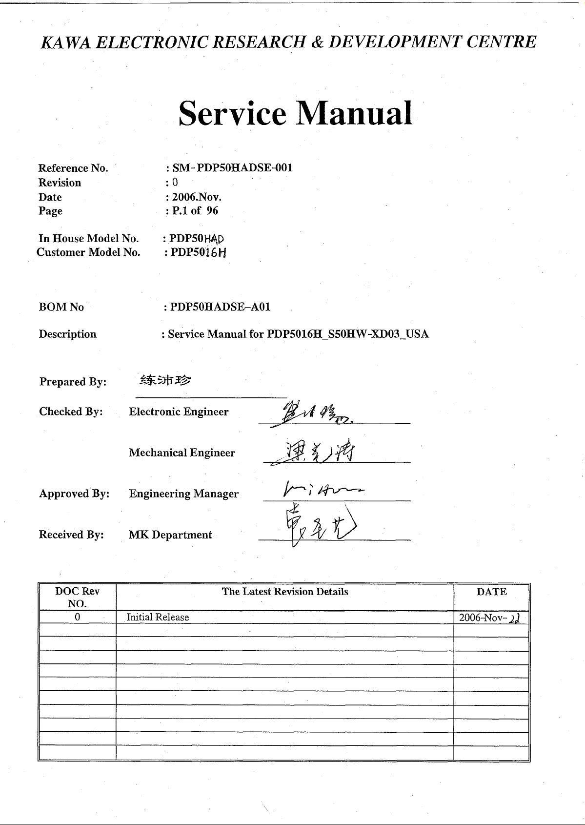
Reference No.
Revision
Date
Page
In House Model No.
Customer Model No.
BOM No
Description
Prepared By:
Checked By: Electronic Engineer
SM- PDP50HADSE-001
0
2006.Nov.
P .lo f 96
PDP50HAP
: PDP5016H
: PDP50HADSE-A01
Service Manual for PDP5016H S50HW-XD03 USA
Mechanical Engineer
Approved By: Engineering Manager
Received By: MK Department
DOC Rev
NO.
0
Initial Release
The Latest Revision Details DATE
t .
2006-Nov-iJ
Page 2
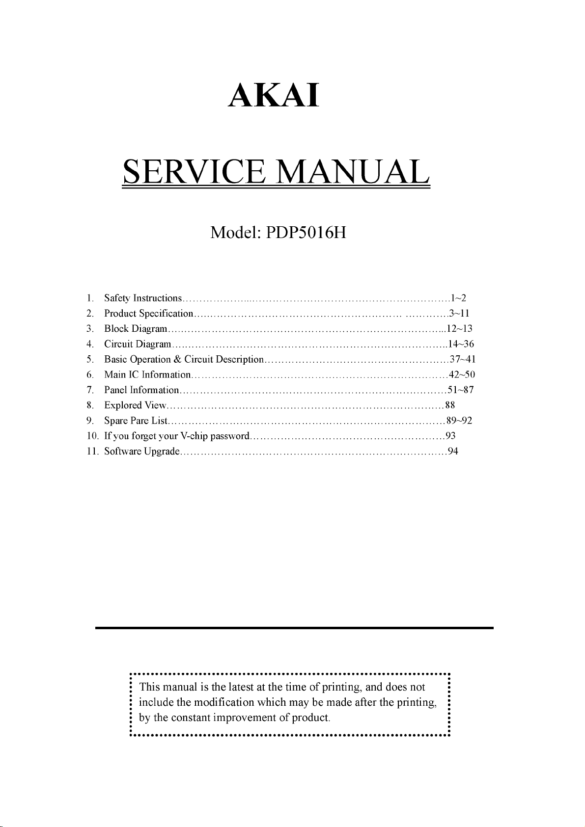
AKAI
SERVICE MANUAL
Model: PDP5016H
1. S afety Instructions............................................................................................................1 ~2
2. Product Specification.......................................................................................................3—11
3. Block Diagram................................................................................................................12—13
4. Circuit Diagram...............................................................................................................14—3 6
5. Basic Operation & Circuit Description..........................................................................37—41
6. Main IC Information....................................................................................................... 42—50
7. Panel Information............................................................................................................51—87
8. Explored View................................................................................................................88
9. Spare Pare List................................................................................................................89—92
10. If you forget your V-chip password
11. Software Upgrade............................................................................................................94
.............................................................................. 93
This manual is the latest at the time of printing, and does not
include the modification which may be made after the printing,
by the constant improvement of product.
Page 3

Safety Precaution
CAUTION
RISK OF ELECTRIC SHOCK
DO NOT O PEN
A
CAUTION: TO REDUCE THE RISK OF
ELECTRIC SH OCK, DO NOT REMOVE COVER
(OR BACK). NO USER-SERVICEABLE PARTS
INSIDE. REFER SERVICING TO QUALIFIED
SERVICE PERSONNEL ONLY.
A
The lightning flash with arrowhead symbol,
within an equilateral triangle, is intended to
alert the user to the presence of uninsulated
“dangerous voltage” within the product’s enclo
sure that may be of sufficient magnitude to
constitute a risk of electric shock to persons.
The exclamation point within an equilateral
triangle is intended to alert the user to the
presence of important operating and
maintenance (servicing) instructions in the
literature accompanying the appliance.
PRECAUTIONS DURING
SERVICING
1. In addition to safety, other parts and
assemblies are specified for conformance with
such regulations as those applying to spurious
radiation. These must also be replaced only
with specified replacements.
Examples: RF converters, tuner units, antenna
selection switches, RF cables, noise-blocking
capacitors, noise-blocking filters, etc.
2. Use specified internal Wiring. Note especially:
1) Wires covered with PVC tubing
2) Double insulated wires
3) High voltage leads
3. Use specified insulating materials for hazardous
live parts. Note especially:
1) Insulating Tape
2) PVC tubing
3) Spacers (insulating barriers)
4) Insulating sheets for transistors
5) Plastic screws fo r fixing micro switches
4. When replacing AC primary side components
(transformers, power cords, noise blocking
capacitors, etc.), wrap ends of wires securely
about the terminals before soldering.
5. Make sure that wires do not contact heat
generating parts (heat sinks, oxide metal film
resistors, fusible resistors, etc.)
6. Check if replaced wires do not contact sharply
edged or pointed parts.
7. Make sure that foreign objects (screws, solder
droplets, etc.) do not remain inside the set.
MAKE YOUR CONTRIBUTION
TO PROTECT THE
ENVIRONMENT
Used batteries with the ISO symbol
\5<9
for recycling as well as small accum ulators
(rechargeable batteries), mini-batteries (cells) and
starter batteries should not be thrown into the
garbage can.
Please leave them at an appropriate depot.
WARNING:
Before servicing this TV receiver, read the
SAFETY INSTRUCTION and PRODUCT
SAFETY NOTICE.
SAFETY INSTRUCTION
The service should not be attempted by anyone
unfam iliar with the necessary instructions on this
apparatus. The following are the necessary
instructions to be observed before servicing.
1. An isolation transformer should be connected in
the power line between the receiver and the
AC line when a service is performed on the
prim ary of the converter transformer of the set.
2. Comply with all caution and safety related
provided on the back of the cabinet, inside the
cabinet, on the chassis or picture tube.
3. To avoid a shock hazard, always discharge the
picture tube's anode to the chassis ground
before removing the anode cap.
4. Completely discharge the high potential voltage
of the picture tube before handling. The picture
tube is a vacuum and if broken, the glass will
explode.
1/ 94
Page 4

5. When replacing a MAIN PCB in the cabinet,
always be certain that all protective are
installed properly such as control knobs,
adjustm ent covers or shields, barriers, isolation
resistor networks etc.
6. When servicing is required, observe the original
lead dressing. Extra precaution should be given
to assure correct lead dressing in the high
voltage area.
7. Keep wires away from high voltage or high
tempera ture components.
8. Before returning the set to the customer,
always perform an AC leakage current check
on the exposed metallic parts of the cabinet,
such as antennas, terminals, screwheads, metal
overlay, control shafts, etc., to be sure the set
is safe to operate without danger of electrical
shock. Plug the AC line cord directly to the
AC outlet (do not use a line isolation
transformer during this check). Use an AC
voltmeter having 5K ohms volt sensitivity or
more in the following manner.
Connect a 1.5K ohm 10 watt resistor paralleled
by a 0.15pF AC type capacitor, between a
good earth ground (water pipe, conductor etc.,)
and the exposed metallic parts, one at a time.
Measure the AC voltage across the combination
of the 1.5K ohm resistor and 0.15 uF
capacitor. Reverse the AC plug at the AC
outlet and repeat the AC voltage measurem ents
for each exposed metallic part.
The measured voltage must not exceed 0.3V
RMS.
This corresponds to 0.5m A AC. Any value
exceeding this limit constitutes a potential
shock hazard and must be corrected
immediately.
The resistance measurem ent should be done
between accessible exposed metal parts and
power cord plug prongs with the pow er switch
"ON". The resistance should be more than
6M ohms.
AC VOLTMETER
PRODUCT SAFETY NOTICE
Many electrical and m echanical parts in this
apparatus have special safety-related
characteristics.
These characteristics are offer passed
unnoticed by visual spection and the protection
afforded by them cannot necessarily be obtained
by using replacement components rates for a
higher voltage, wattage, etc.
The replacement parts which have these
special safety characteristics are identified by A
marks on the schematic diagram and on the parts
list.
Before replacing any of these components,
read the parts list in this manual carefully. The
use of substitute replacement parts which do not
have the same safety characteristics as specified
in the parts list may create shock, fire, or other
hazards.
9. Must be sure that the ground wire o f the AC
inlet is connected with the ground of the
apparatus properly.
Good earth ground
such as the water
- pipe, conductor,
etc.
AC Leakage Current Check
1500 ohmi, lOwatt
Place this probe
on each exposed
metallic part
2/ 94
Page 5
Technical Specifications
M O D E L i PDP-5G16
5 0 ” P la s m a D is p la y
DATE FIRST ISSUED ISSUE
1
REVISIONS
ISSUED DATE DESCRIPTION RAISED BY i
RAISED BY CHECKED BY NUMBER OF PAGES
9
SPECIFICATION AGREED : SIGNATURE DATE
R & D DEPARTMENT
COMMERCIAL DEPARTMENT
PRODUCTION DEPARTMENT
Q/A DEPARTMENT
CUSTOMER
SPECIFICATION APPROVED : SIGNATURE : DATE
NOTE : Only d o cu m e nts sta m p ed “Co n tr o lled D o c u m en t” to b e u sed fo r m a nu factu r e of p rod u c tion p arts.
3/ 94
Page 6

CONTINUATION PAGE
Technical Specifications
1. S ta n d a r d T e s t C o n d itio n s
PDP-5016
NUMBER 2 OF 9 PAGES
All tests shall be performed under the following conditions, unless otherwise specified.
1.1 Ambient light
1.2 Viewing distance
1.3 Warm up time
1.4 PDP Panel facing
1.5 Measuring Equipment
1.6 Magnetic field
1.7 Control settings
1.8 Power input
1.9 Ambient temperature
1.10 Display mode
150ux (When measuring IB, the ambient luminance
= 0.1Cd/m2)
50cm in front of PDP
30 minutes
no restricted
PC, Chroma 2225 signal generator (with Chroma digital
additional card) or equivalent, Minolta CA100 photometer
no restricted
Brightness, Contrast, Tint, Color set at Center(50)
100~240Vac
20°C ± 5°C (68°F ± 9°F)
31.5KHz/60Hz (Resolution 1366 x 768)
1.11 Other conditions
1.11.1 With image sticking protection of PDP module, the luminance will descend
by time on a same still screen and rapidly go down in 5 minutes. When
measuring the color tracking and luminance of a same still screen, be sure t
o accomplish the measurement in one minute to ensure its accuracy.
1.11.2 Due to the structure of PDP, the extra-high-bright same screen should not
hold over 5 minutes for fear of branding on the panel.
4/ 94
Page 7

Technical Specifications
E L E C T R IC A L C H A R A C T E R IS T IC S
2. P o w e r In p u t
PDP-5016
CONTINUATION PAGE
NUMBER 3 OF 9 PAGES
2.1 Voltage
2.2 Input Current
2.3 Maximum Inrush Current
Test condition
2.4 Frequency
2.5 Power Consumption
Test condition
2.6 Power Factor
2.7 Withstanding voltage
3. D is p la y
3.1 Screen Size
3.2 Aspect Ratio
3.3 Pixel Resolution
3.4 Peak Brightness
3.5 Contrast Ratio (Dark room)
3.6 Viewing Angle
3.7 OSD language
100 ~ 240VAC
5.0 /2.5A
<30 A (FOR AC110V ONLY)
Measured when switched off for at least 20 mins
50Hz to 60Hz(±3Hz)
< 480W
full white display with maximum brightness and
contrast
Meets I EC 1000-3-2
1.5kVac or 2.2kVdc for 1 sec
50” Plasma display
16:9
1366x768
1000 cd/m2 (Panel module without filter)
4000:1 (Panel module without filter)
Over 160°
English
4. S ig n al
4.1 TV/AV & Graphic input
4.1.1 TV standard
4.1.2 TV Tuning system
4.1.3 CATV
4.1.4 Composite signal
4.1.5 Y,C Signal
4.1.6 Component signal
4.1.7 Graphic I/P
4.1.8EDID compatibility
4.1.9 I/P frequency
NTSCM,PAL/N,PAL/M
PLL 181CH
125CH
CVBS
S-Video
Y, Pb/Cb, Pr/Cr, HDTV compatible
Analog: D-sub 15pin detachable cable
Digital: DVI
DDC 1.3
fH 31.5kHz to 60kHz/fV: 56.25Hz to 75Hz (1024X768
recommended)
5/ 94
Page 8

Technical Specifications
4.2 Audio input
Audio I/P(L/Rx5)
4.3 AV output
Audio&Video O/P(RCAx3)
PDP-5016
1 for DVI / D-Sub
1 for Y/ Pb/Pr
1 for Y/ Cb/Cr
1 for CVBS
1 for S-Video
: Monitor out(Video & Audio L/R)
CONTINUATION PAGE
NUMBER 4 OF 9 PAGES
4.4 Other function :
5. E n v ir o n m e n t
5.1 Operating environment
5.1.1 Temperature :
5.1.2 Relative humidity:
5.2 Storage and Transport
5.2.1 Temperature :
5.2.2 Relative humidity:
6. P a n e l C h a r a c te r is tic s
6.1 Type
6.2 Size
6.3 Aspect ratio
6.4 Viewing angle
6.5 Resolution
6.6 Weight
6.7 Color
6.8 Contrast
6.9 Peak brightness :
PIP/POP/PBP, Picture size, Picture Still, Sound mode,Last
memory, Timer, MTS
5° to 33°C
20% to 85%(non-condensing)
-20°C to 60°C(-4° to 140°F)
5% to 95%
S50HW-XD03
50”, 1190mm(width)x7005mm(height)x59mm(depth)±1
mm)
16:9
Over 160°
1366X768
22.0kg ±0.5 kg (Net)
1024(R)X1024(G)X1024(B) COLORS
Average 60:1 (In a bright room with 150Lux at center)
Typical 5000:1 (In a dark room 1/100 White Window
pattern at center).
Typical 1000cd/m2 (1/25 White Window)
6.10 Color Coordinate Uniformity :
Test Pattern :
Contrast; Brightness and Color control at norma
setting
Full white pattern
Average of point A,B,C,D and E +/- 0.01
6/ 94
Page 9

Technical Specifications
PDP-5016
NUMBER 5 OF 9 PAGES
6.11 Color temperature : Contrast at center (50); Brightness center (50);
Color temperature set at Natural
x=0.285±0.02
y=0.290±0.02
6.12 Cell Defect Specifications
Subject to Panel supplier specification as appends.
7. F ro n t P an e l C o n t ro l B u tto n
CONTINUATION PAGE
7.1 CH Up / Down Button
Push the key to changing the channel up or down.
When selecting the item on OSD menu.
Volume Up/ Down Button
Push the key to increase the volume up or down.
When selecting the adjusting item on OSD menu
increase or decrease the data-bar.
Menu Button
Source Select Button
7.2 Stand by Button
Enter to the OSD menu.
Push the key to select the input signals source.
Switch on main power, or switch off to enter power
Saving modes.
7.3 Main Power Switch
8. O S D F u n c tio n
Turn on or off the unit.
8.1 Picture : State (Normal,Dark,Bright,User); Display (Bright,contrast,Color,Hue)
Temp (warm,Cool,Normal,User);
Position (H-posit,V-posit,Phase,H-size,Auto Adjust)
8.2 Sound : Setup (Mode,AVC,Volume,Balance);
Equalizer (120HZ,500HZ,1.5KHZ,5KHZ,10KHZ)
BBE Setup (Gain,Treble,Bass)
8.3 OSD : Size (Panorama,16:9,Normal,Anamorphic,Letter Box,TV Mode)
OSD Set (Language,OSD Position,Time Out)
Option (Burn Protect, Version)
V-Chip , C/C
8.4 Layout : Layout (Full Screen,PIP,Split Screen,Grid,POP 3,POP 12)
PIP Set (Sub Win Source,Sub Win Size,PIP Size.PIP Position)
8.5 Time : Sleep (30Min,60Min,90Min,120Min,180Min)
Wake Up (Time Edit,Volume,TV Mode,Channel)
Time Set
8.6 TV Set : TV Set (Auto Search,Manul Search,System,MTS,Auto Fine,Fine)
CH Edit
7/ 94
Page 10

Technical Specifications
9. A g e n c y A p p r o v a ls
Safety UL60950
Emissions FCC class B
10 . R e lia b ility
PDP-5016
CONTINUATION PAGE
NUMBER 6 OF 9 PAGES
11.1 MTBF
11. A c c e s s o rie s
20,000 hours(Use moving picture signal at 25°C ambient)
User manual x1, Remote control x1, Stand x1, Power cord x1,
Battery x 2, Accessories box x 1 ,Speaker x 2,Speaker wire x2
8/ 94
Page 11

Technical Specifications
12. Support the Signal Mode
A. D-Sub Mode (VGA or DVI)
PDP-5016
CONTINUATION PAGE
NUMBER 7 OF 9 PAGES
NO.
Resolution
1 640 x 400
2
3
4
5
6
7
8
9
10
11
12
13
14
15
16
17
18
19
640 x 480
640 x 480
640 x 480
640 x 480
720 x 400
800 x 600
800 x 600
800 x 600
800 x 600
832 x 624
1024x 768
1024x 768
1024x 768
1152x 864
1152x 864
1152x 864
1280x 960
1280x 1024
Horizontal
Frequency
Frequency
(KHz)
31.47 70.08
31.50 60.00
35.00 67.00
37.50 75.00
37.86 72.81
31.47 70.08
35.16 56.25
37.90 60.32
46.90 75.00
48.08 72.19
49.00 74.00
48.40 60.00
56.50 70.00
60.00 75.00
54.53 61.13
63.86 70.02
Vertical
(Hz)
Dot Clock
Frequency
(MHz)
25.17
25.18
30.24
31.50
31.50
28.32
36.00
40.00
49.50
50.00
57.27
65.00
75.00
78.75
80.37
94.51
67.52 75.02
60.02 60.02 108.04
64.00 60.01 108.00
108.03
B. DTV Mode
NO. Resolution
1 480 i
2
3
4
5
6
7
8
1080i(1920x1080)
1080i(1920x1080)
576 i
480p(720x480)
576p(720x576)
720p(1280x720)
720p(1280x720)
Horizontal
Frequency
Frequency
(KHz)
15.734 59.94
15.625 50.00
31.468 59.94
31.25 50.00
45.00 60.00
37.50 50.00
28.125 50.00
33.75 60.00
Vertical
(Hz)
Dot Clock
Frequency
(MHz)
13.50
13.50
27.00
27.00
74.25
74.25
74.25
74.25
- When the signal received by the Display exceeds the allowed range, a warning message "Out Of Range”
shall appear on the screen.
- You can confirm the input signal format from the "OSD Menu”.
9/ 94
Page 12

Technical Specifications
13. R e m o t e C o n tro l
PDP-5016
CONTINUATION PAGE
NUMBER 8 OF 9 PAGES
1 Power ( 6 ): Press to turn on and off.
2 Mute ( ^ ): Press to mute the sound. Press
again or press ► to restore the sound.
3 P.STILL: Press to freeze the picture. Press
again to restore the picture.
4 P.SIZE: Press to cycles through the picture
size: Normal, Fill Screen, Anamorphic,
Letter Box or TV Mode, Panorama..
5 P. MODE: Press to cycles through the
picture mode: Normal, Bright, Dark, User.
6 S.SELE: Press to cycles through the sound
select: Main window sound or Sub window
sound.
7 PIP: Press to turns on PIP (picture-in-
picture) feature. Such as Full Screen, PIP or
Split Screen.
8 SWAP: Press to switches the Main window
or Sub window pictures.
9 PIP CH+ : Press to select Sub window
Channel Up.
PIP CH- : Press to select Sub window
Channel Down.
10 TIME: Press to display the current time.
11 SLEEP: Press repeatedly until it displays
the time in minutes (30 Min, 60 Min, 90 Min,
120 Min, 180 Min or Off ) that you want the
PDP to remain on before shutting off. To
cancel Sleep Time, press SLEEP repeatedly
until Sleep Off appears. And you can press
■4 or ► to select sleep time shut down.
12 MTS: Press repeatedly to cycle through the
Multi-channel TV sound (MTS) options:
Mono, Stereo and SAP (Second Audio
Program).
13 INFO: Press to display on-screen information. Press it again to turn the display off.
14 CH Erase, CH Save buttons: Press to erase or save channel.
10 C/C: Press to select the Closed Caption mode.
10 V-Chip: Press to select the child protect mode.
17 Number buttons: Press 0~9,100 to select a channel; the channel changes after 2
seconds.
10 PIP Source: Press to select the signal for Sub Window.(Only for PIP.)
10 F.WHITE: Press to show a full white picture.
20 PREV: Press it returns to the last viewed channel.(Only for TV.)
1
3
4
7
8
10
11
14
28
-GD
P.STILL P.SIZE P.MODE S.SELE
TZD C 3 c g CZh
O P Q Q
TIME SLEEP
a p æ
Ç 3Ç 3C qC 3-
© © ©
© © ©
© © ©
©
PIP source F.Whlte PREV
O ÇJ Œ l
SOUND PICTURE EXIT
- a □ en im
------
~ ir
100
□
------
15
10/94
(Continued on next page)
Page 13

CONTINUATION PAGE
Technical Specifications
PDP-5016
NUMBER 9 OF 9 PAGES
21 SOUND: Press to select different sound system, such as Normal, Flat, News, Cinema,
User or BBE Digital.
22 PICTURE: Press to select “BRIGHTNESS”, “COLOR”, “CONTRAST”, ”HUE” or
“SHARPNESS”, and you can use A or ► to adjust.
23 EXIT: Press to return or exit OSD menu.
24 SOURCE: Press to select the signal sources directly. Such as TV, AV1, S-VIDEO,
YCbCr, YPbPr, Analog RGB or Digital RGB.
23 MENU: Press to display the OSD Menu.
23 OK: Press to enter or confirm.
21 ▲ / ▼ : They are used as ▲ / ▼ buttons in the OSD Menu screen and they can be
used for the selection of the program when the OSD Menu is not shown on the screen.
23-4 / ► : They are used as -4 / ► buttons in the OSD Menu screen and they can be
used for the adjustment of volume when the OSD Menu is not shown on the screen.
P H Y S IC A L C H A R A C T E R IS T IC S
14. P o w e r C o r d
Length : 1.8m nominal
Type :
15. C a b in e t
optional
15.1 Color : silver colour as defined by colour plaque reference number
15.2 Weight
Net weight :
Gross weight :
51.8kg
74kg
15.3 Dimensions (w/o stand&handles)
Width :
Height :
Depth :
1227.8mm
739.8mm
122.7mm
11/94
Page 14
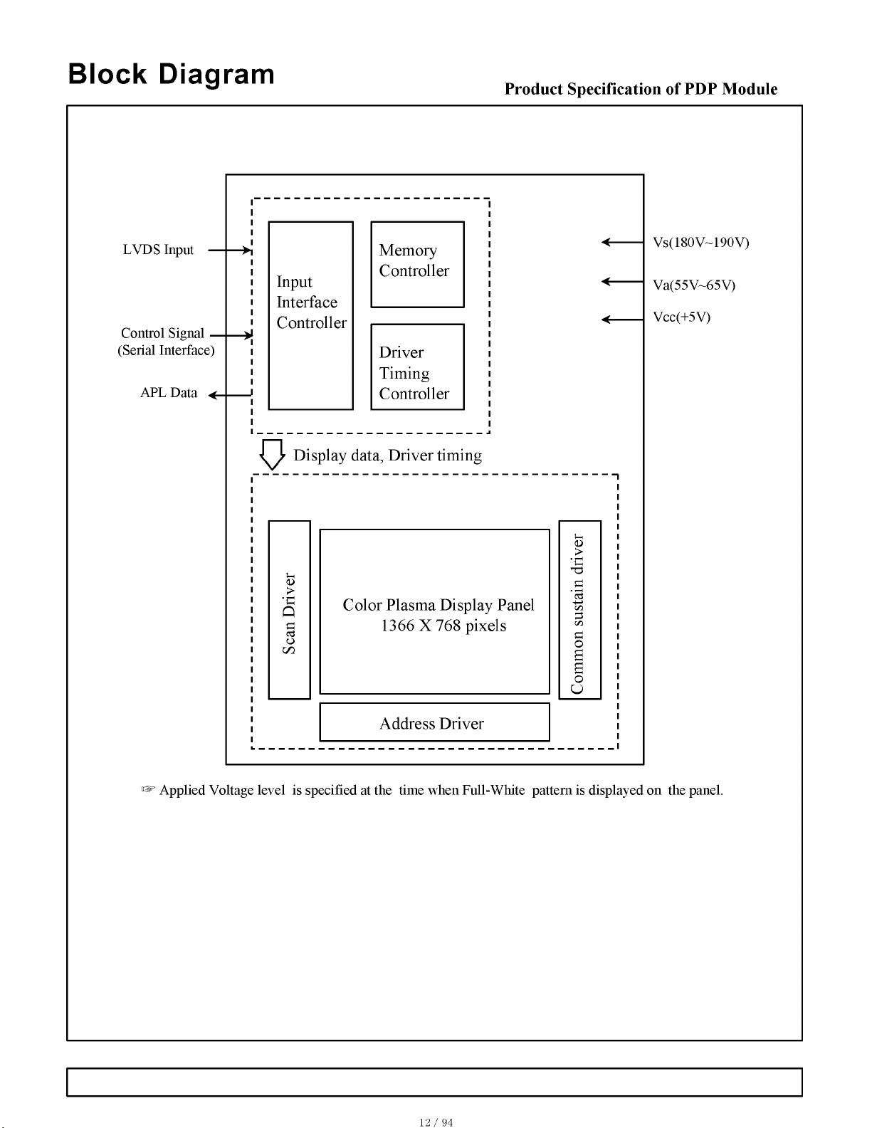
Block Diagram
Product Specification of PDP Module
LVDS Input
Control Signal —
(Serial Interface)
APL Data
Memory
Input
Interface
Controller
Display data, Driver timing
>
•c
Q
G
cd
O
GO
Controller
Driver
Timing
Controller
Color Plasma Display Panel
1366 X 768 pixels
<u
>
•G
T3
cö
3
c
O
a
a
o
O
Vs(180V~190V)
Va(55V~65V)
Vcc(+5V)
Address Driver
Applied Voltage level is specified at the time when Full-White pattern is displayed on the panel.
12/ 94
Page 15

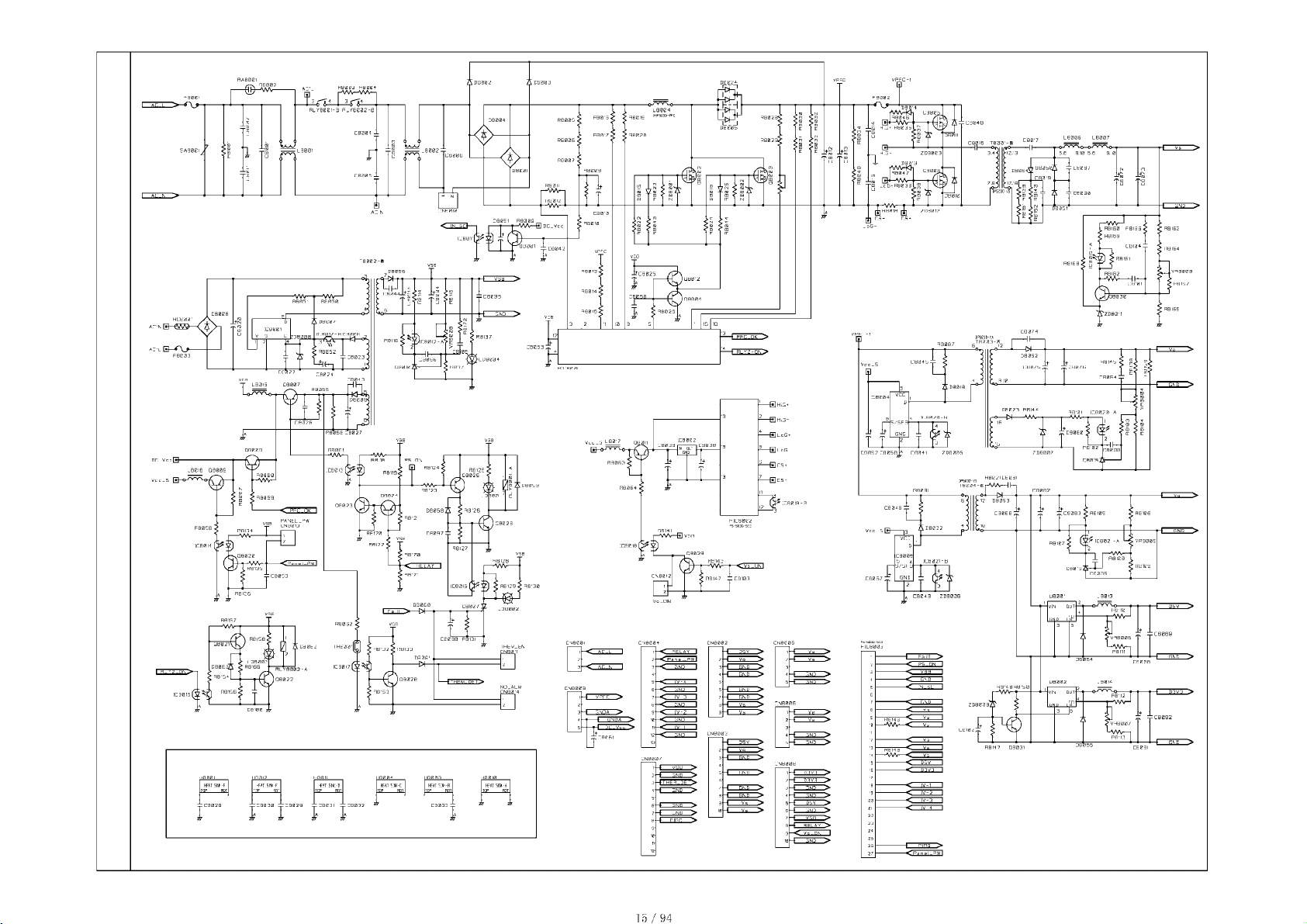
Block Diag ram MAIN/AUDIO BOARD
13/ 94
Page 16
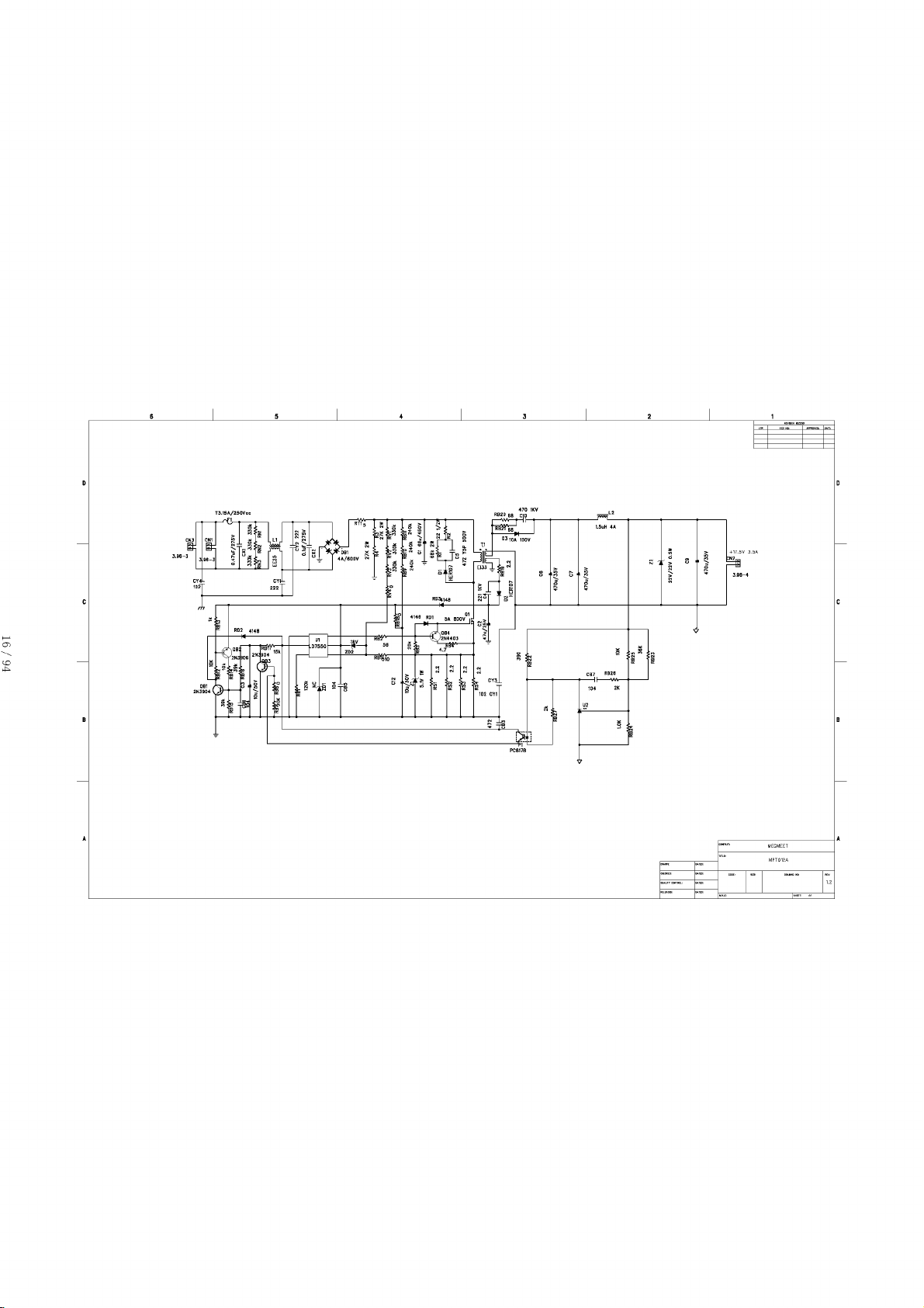
Circuit Diagram
- Power supply board o f A u d io A m p lif ier ,
- Main (Vi de o ) board
- A ud i o /T u n e r board
- Ke yp ad b oard
- Remote control rec eiv er board
- Rem ot e contro l board
14/ 94
Page 17

MP T0 12 A
Page 18
15/94
Page 19
1
16 / 9 4
Page 20
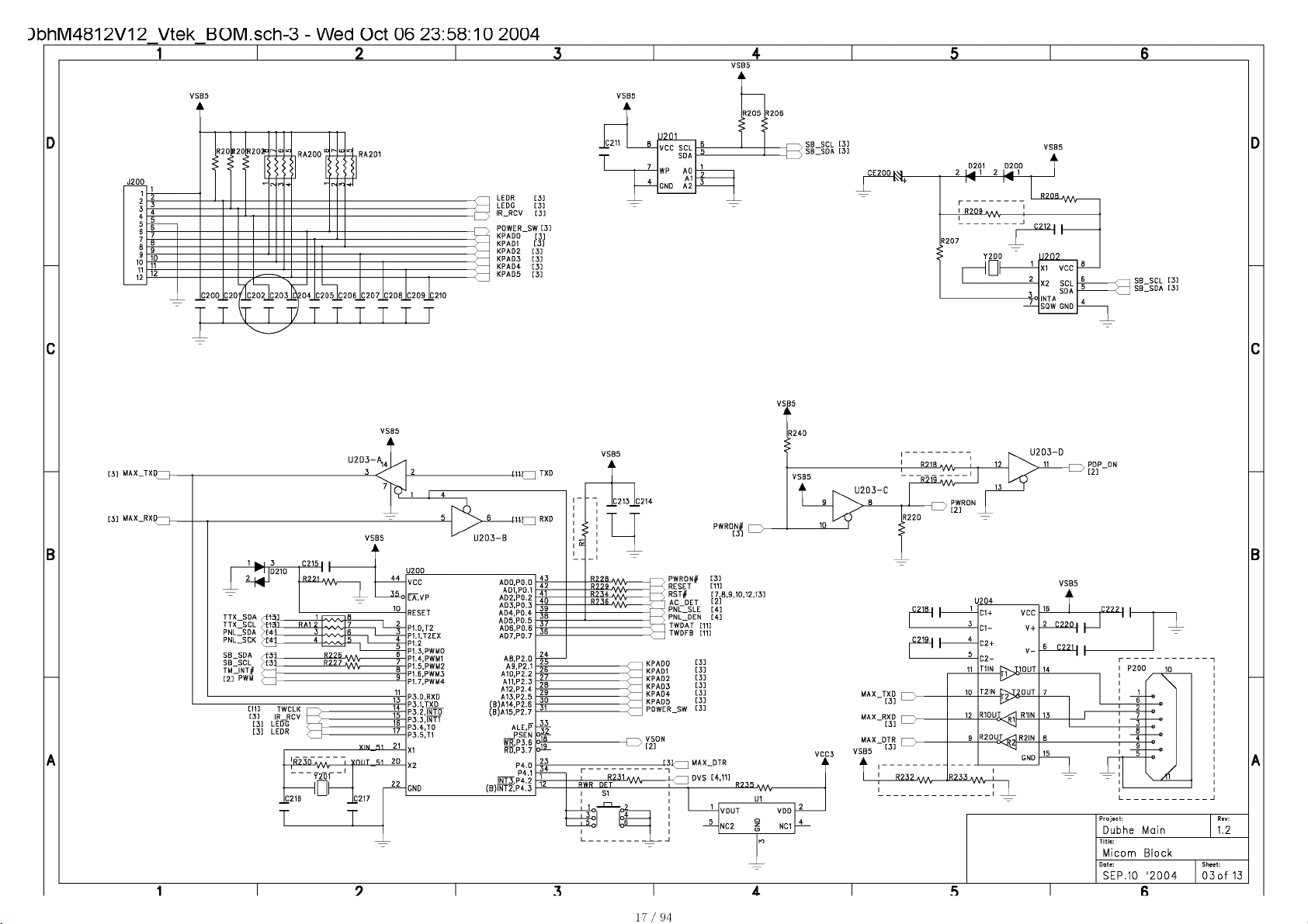
DbhM4812V12 Vtek BOM .sch-3 - Wed Oct 06 23:58:10 2004
17/ 94
Page 21
DbhM4812V12 Vtek BOM .sch-4 - Wed Oct 06 23:58:11 2004
DDF[00:23]
~m
------
DDF07/
11
nnFon,
10
DDFOL
9
psbi
. DF04 1
» DF05 ? 7 RDFilfi
„ DFOB 3
» DF07 4
„ DFOB 1
» DF09 7 7 DnFns,
„ dfio 3 B RDF10/
» DF11 4
„ DF17 1
» DF13 7
. HF14 3
» DF15 4
„ DF1B 1
. DF17 2
v DF18 3
„ nFiq 4 5 DDF19,
„ DF70 1
„ DF71 7
v DF22 3
, DF23 4
'S/VS/
I
A252
/wv
'S/VS/
A253
/yvv
/wv
FA254
/yvv
I
FA255
—:
1
b DnF04,
b onFnfi,
5 nnFnz
B DDFOfl.
5 RDF11 .
B DDF17/
7 DHF13/
6 DDF14/
5 DHF15,
R DDF16.
7 DDF17,
R DDF18.
fi DDF20.
7 DDF21,
fi DDF2Z
5 DDF23,
DDF07,
-| 17
IÎDF0.1
11
in DDF04,
nnFos,
DDF14,
I17
imîfis.
in nOFOR,
n0F09,
DDF10/
I17
IÎDF11 ,
in I50F17/
DDF13,
DDF22,
i1?
DDF23,
11
DDF16,
10
DDF17,
DDF18,
l1?
DDF19,
11
DDF20,
10
DDF21,
9
nnsn7.
11
10 nnsoa
nnsm.
nnso7,
I17
nnsn.\
10 ODSfH,
IÎDS05.
9
[4TD1+
nnsu,
I17
DDS15/
10 nnsna,
nnsns,
DDS10,
I17
IÎDR11 ,
10
IÎDS17,
IÎDR1.T,
DDS2Z
I17
DDS23.
DDS16,
10
DDS17,
DDS18.
-|1?
DDS19,
11
DDS20.
10
DDS21,
9
[4 A2-
[4fA2+
[4ÎB2-
[4TB2+
FOR DUAL THINE FORMAT
. DDF01 52
. DDF02 54
. DDF03 55
. DDF04 56
. DDF05 3
. DDF08 50
. DDF07 2
. DDF08 4
. DDF09 6
. DDF10 7
. DDF11
. DDF12 12
. DDF13 14
. DDF14 B
. DDF15 10
. DDF16 15
. DDF17 19
. DDF1B 20
. DDF19 22
. DDF20 23
. DDF21 24
. DDF22 16
. DDF23 1B
11
>CL KIN PVCC
TA0(R2,RD)
TA1(R3,R1)
TA2(R4,R2)
TA3lR5,R3)
TA4(R6,R4) VCC1
TA5(R7,R5) VCC2
TD0(R0,R6) RS(VCC)
TD1(R1,R7)
TA6ÎG2.G0) TXOUTG—
TB0(G3,G1) TXOUTO+
TB1(G4,G2)
TB2(G5,G3) TXOUT1-
TB3 G6.G4) TXOUT14
TB4 G7.G5)
TD2 G0,G6) TXOUT2-
TD3(G1,B7)
TB5(B2,B0)
TB6(B3,B1)
TC0(B4,B2) TX0UT3-
TC1(B5,B3) TX0UT3+
TC2(B6,B4)
TC3 B7.B5) GND1
TD4 B0.B6) GND2
TD5(B1,B7)
TC4(HS)
TC5 VS) 0GND1
TC61EN) 0GND2
TD6(RES) 0GND3
R FB (THINE,NS) PgnD1
PWRDN# PGND2
LVDSVCC
TXOUT2+
TXCLK-
TXCLK+
GND3
GND4
GND5
-R
TA1+
[4]
TB1- [4]
TB1+
[4]
TCI—[4]
TC1+ [4]
TCLK1—[4]
TCLK1-K4]
TD1-
[4]
TD1+
[4]
. DDSOB' 4
. DDS091 6
. DDS101 /
. DDS11 1
. DDS121 17
. DDS131 14
. DDS141 H
. DDS151
. DDS161 15
. DDS171 19
. DDS181 70
. DDS191 22
11
11)
1
>CLKIN PVCC
TA0(R2,R0)
TA1(R3,R1) LVDSVCC
TA2(R4,R2)
TA3(R5,R3)
TA4 R6,R4) VCC1
TA5 R7,R5) VCC2
TD0(R0,R6) RS(VCC)
TD1(R1,R7)
TA6(G2,G0) TXOUTO—
TB0(G3,G1) TXOUTO+
TB1(G4,G2)
TB2(G5,G3) TX0UT1-
TB3(G6,G4) TX0UT1+
TB4(G7,G5)
TD2(GD,G6) TX0UT2-
TD3(G1,G7) TX0UT2+
TB5(B2,B0) TXCLK+
TB6fB3,Bl)
TCD(B4,B2)
TC1(B5,B3) TX0UT3+
TC2(B6,B4)
TC3(B7,B5) GND1
TD4(BD,B6) GND2
TD5(B1,B7) GND3
TC4(HS)
TC5 VS) 0GND1
TC6ÎEN) 0GND2
TD6(RES) 0GND3
R FB (THINE,NS) pGND1
PWRDN0 PGND2
TXCLK-
TX0UT3-
GND4
GND5
TA2-
[4]
TA2+
[4]
TB2- [4]
TB2+
[4]
TC2-
[4]
TC2+[4]
- [4]
TCLK2
-R
TCLK2+ [4]
TD2-
St
-R
Project:
Dubhe Main
Title:
TTL & LVDS Output
Date: Sheet:
TD2+
[4]
[4]
SEP.10 '2004 04 of 13
Rev:
1.2
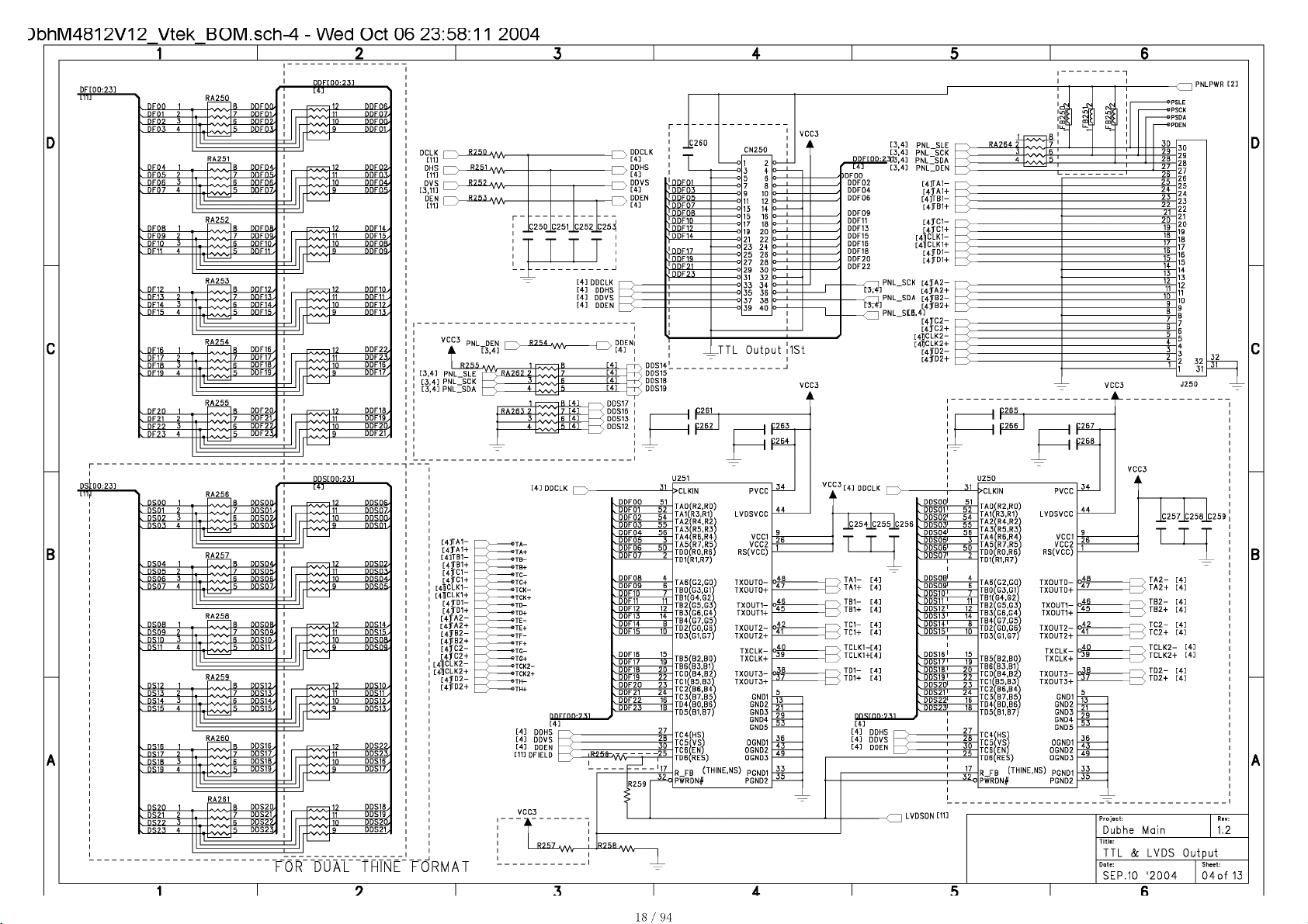
18/ 94
Page 22
3bhM4812V12 Vtek BOM.sch-5 - Wed Oct 06 23:58:15 2004
19 / 94
Page 23
DbhM4812V12 Vtek BOM .sch-6 - Wed Oct 06 23:58:16 2004
O j
C411 jc^412_jc413_jc414Jc 415 Jc416 Jc 417 +
TTTTTT“M
PV
03
c
p
Ç41BjÇ419 +iï
CE400
:E401
?
2
1
■— 1—
JÇ420JÇ421JÇ422
io ^ T T T 1
[5] GHSYNC
Jc42
I
[5] GVSYNC
HDPRIN I
HDYIN I
HDPBIN I
GRAIN I--y_
GGAIN I--s_
[5] '
[5] '
[5] '
[5] '--^
rm 1
----
^
Jc42
I
__
— U401
2
S1A VCC
SIR
SIC
sin
S2A DD
S2B IN
S2C ËN
S2D GND
H \~
DA
DB
DC
VCC5
A
«FB40Q,
[8.11.12] SDA3G I
[8.11.12] 5CL3G
[11]
[11]
R40B w
K4P9 w
R41P w
----
----
----
-PV&3
C403| |
C404 | |
C405 | |
jc408_Jc4l
-----
Q
R40CT"
|
------
------
------
------
;
C4Q0
o
o it cm ro m to r- oo oi orrcMr'wm oz;
SDA REDO
SCL RED1
A0 RED2
CLAMP
COAST RED5
HSYNC RED6
VSYNC RED7
§+-
RAIN
4L
GAIN
43.
BAIN
49.
50GIN
AVD3
VCC3
A
ld in in to ^
U400 GREEN0
DATACLK
S0G0UT
HS0UT
VS0UT BLUE6
REFBYPASS
M!DSCV0
ÛQÛQÛQQÛQÛQÛÛQQÛQQQÛ
zzzzzzzzzzzzzzzzzzzz
CJ UU UUU UU UUU UU UCD UU UU U
PVD3
Q
RED3
RED4
GREEN1
GREEN2
GREEN3
GREEN4
GREEN5
GREEN6
GREEN7
BLUE0
BLUE1
BLUE2
BLUE3
BLUE4
BLUE5
BLUE7
VCC5
A
7fi RA40©
/h 3
74
73 1 -
RA4019
r?
71 3
/O
9 1 r
RA40Z>
K
/
6
5 1 -
4 RA403>
A
?
19 1 r
1H RA404?
17
IK
15 1 h
14 RA40®
13 3
12
4
4
3
4
3
4
3
4
4
B
fi
8
6 RRRROft
5
1R
7
fi
5 GRGR11,
8 BRRR19,
7 GRGB13/
fi
5
18
6
18
6 GRGR7Z
fi
RGB[00:07] - Red
RGB[08:15] - Green
RGB[16:23] - Blue
GRGB0L
GRGR07.
GRGB0.1
GRGR04
RRRROfi
GRGR07,
GRGBOa
RRRROft
RRRR10/
RRRR14/
GRGR15/
GRGR16/
RRRR17/
GRGR1B/
RRRR19,
GRGR7C1
RRRR71/
GRGB23
GRGBrOD:231
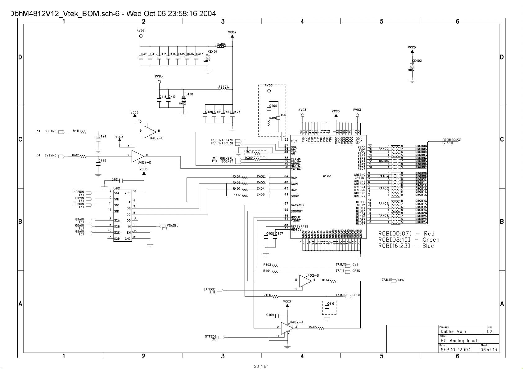
20/ 94
^402-A
3
-----
7
U4D2-B
6
---
R4Q5 VNAr~
Elli-wV-
JC4
[7.8.11|3—> GVS
[7.11] |--> GFBK
[7.6.1^ GHS
Project:
Dubhe Main
Title:
PC Analog Input
Date: Sheet:
Rev:
1.2
SEP.10 '2004 06 of 13
Page 24
DbhM4812V12 Vtek BOM .sch-7 - Wed Oct 06 23:58:18 2004
JL
RX2+ I--v_
RX2- |—p
[5]
RX1 + I—v_
[5]
RX1- h^C
RX0+
RX0-
RXC+
R-
RXC-
DVLSCL I—>
DVLSDA I—. R460 » a a
GDFEOE I--\
[3,B,9,10,12,13J '--7 vv^
---
[5.11] '—7 vvv^
[5.11] '—7 vvv^
[11] '--^
RST# i-^
R459 VW-
______
---
VCC3
A
R458 R457 [R456 R454 R453
RX2P
RX2M
RX1P
RX1M
RXOP
RXOM
RXCP
RXCM
OCKJNV/SCL
ST/SDA
PDÜ"
PD
STAG_0UT
SCAN
DFO/RST#
PIXS
CTL1/KSCL
CTL2/KSDA
VCC3
A
C4SsJç*SS_£45’j:+SeJçJS9jç460_Ë+SlJç'
TTTTTTT
10 1 r
QEO
11 RA4503
QE1
12 3
QE2
13
QE3
14 1
QE4
15 RA4519
QE5
16 3
QE6
17
QE7
20 1
QE8
21 RA457?
QE9
22 3
0 E10
23
QE11
24 1
Q E12
25 RA453?
QE13
26
QE14
27
QE15
30 1
QE16
31
QE17
32 3
QE18
33
QE19
34 1
QE20
35
0E21
36 3
QE22
37
QE23
49
50
51
4
4
4
3
4
RA4549
4
RA45S
4
RGB[00:07]
RGB[08:15]
RGB[16:23]
7
7
7
8
7
R
P
7
R
7
5
RRRRH1
RRRRH5
RRRR07
Red
Green
Blue
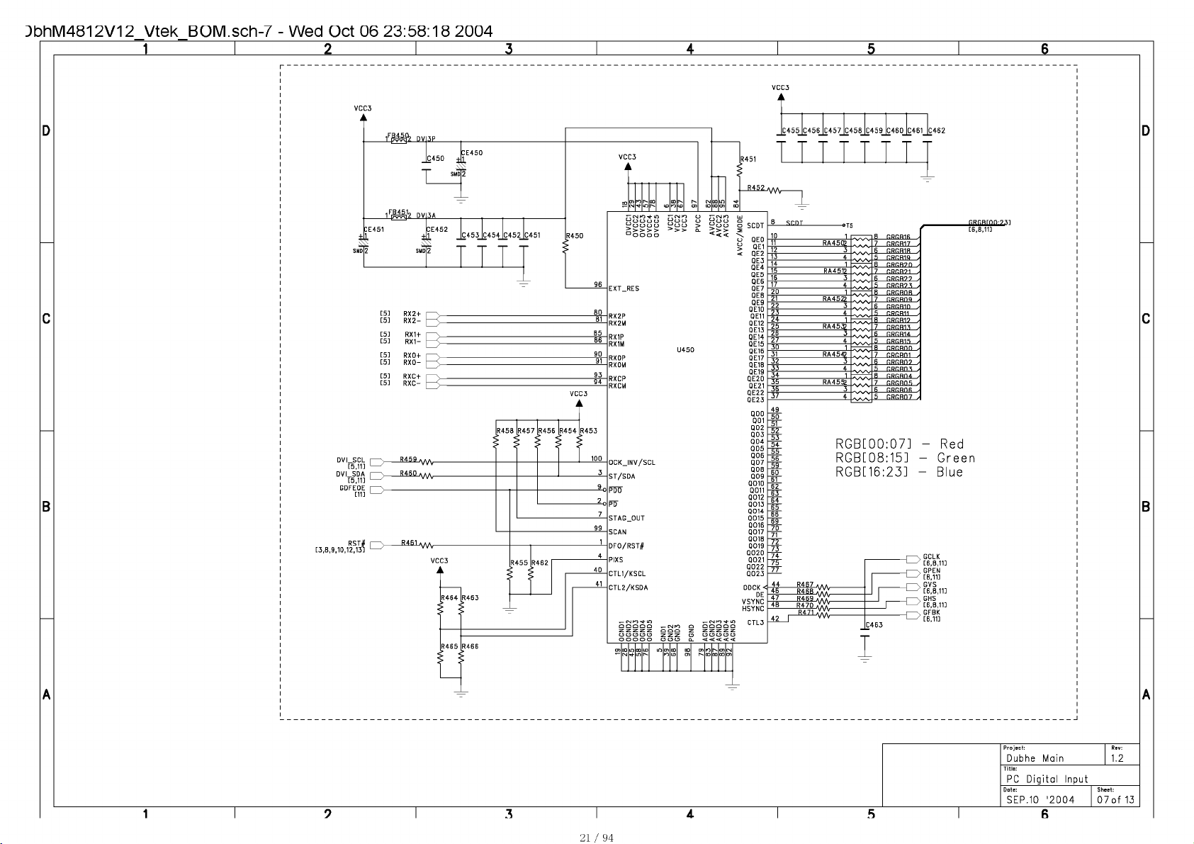
21/ 94
O Q OQ Q
Project:
Dubhe Main
Title:
PC Digital Input
Date: Sheet:
Rev:
1.2
SEP.10 '2004 07 of 13
Page 25
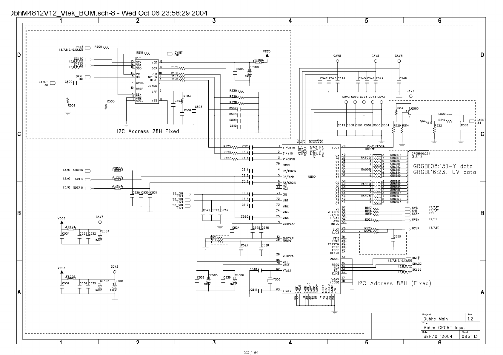
DbhM4812V12 Vtek BOM .sch-8 - Wed Oct 06 23:58:29 2004
22/ 94
Page 26
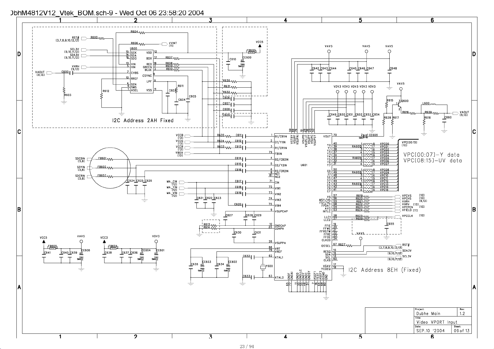
DbhM4812V12 Vtek BOM .sch-9 - Wed Oct 06 23:58:20 2004
23/ 94
Page 27
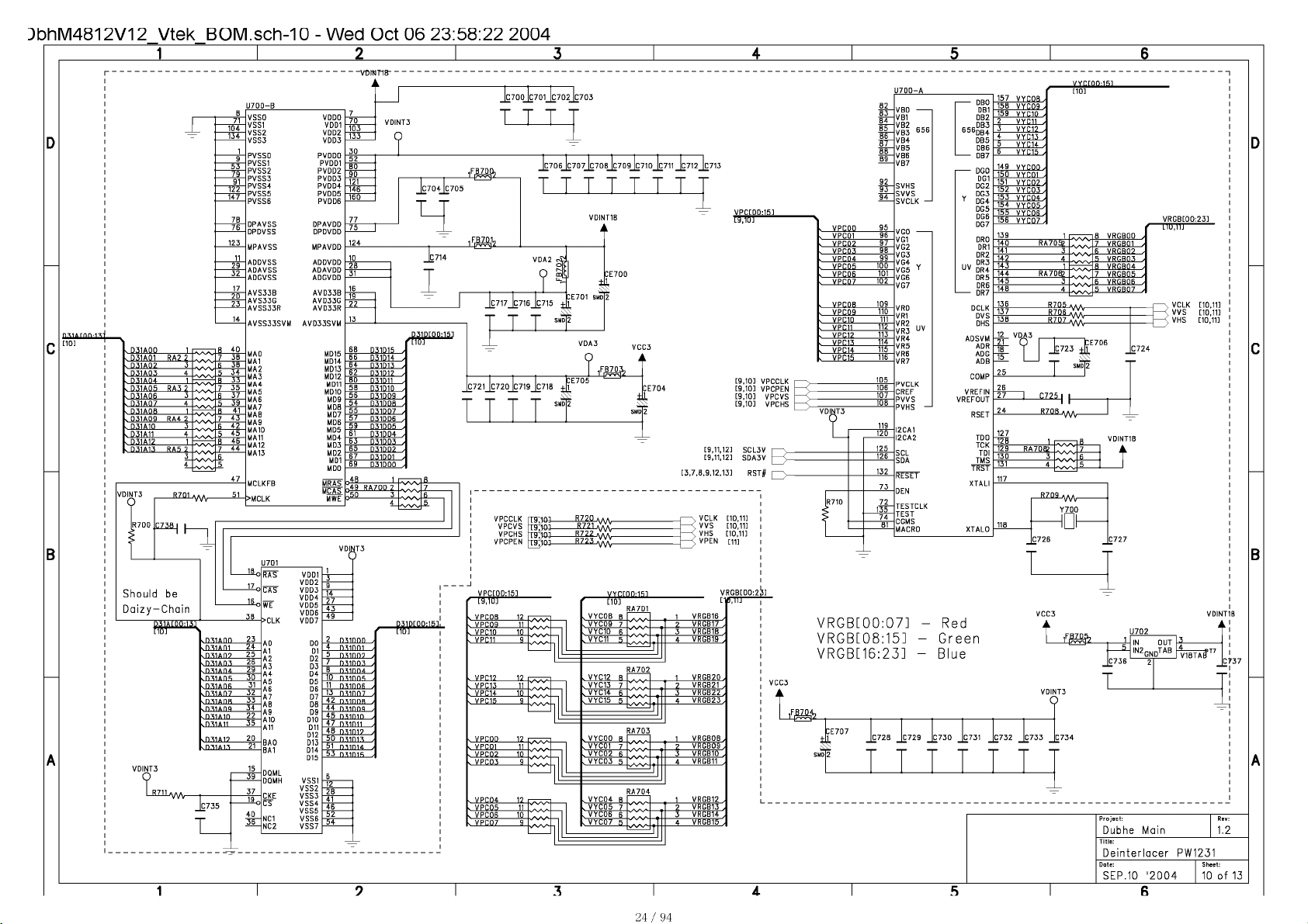
DbhM4812V12 Vtek BOM.sch-10 - Wed Oct 06 23:58:22 2004
„ D31A01 RA? ?
„ 031A07
, D31A03 4
< D31A04 1
, D31A05 RA3 ?
„ 031A06
< D31AQ7 4
. D31A0B 1
„ 031A09
RA4 2
, D31A10
, D31A11 4
. D31A12 1
V D31A13 RA5 2
0 C75B|
Should be
Daizy-Chain
3
3
3
'
C735
r
VSSO VDDO
_
71
VSS1 VDD1
104
VSS2 VDD2
134
VSS3 VDD3
PVSSO PVDDO
PVSS1 PVDD1
PVSS2 PVDD2
PVSS3 PVDD3
PVSS4 PVDD4
122
PVSS5 PVDD5
147
PVSS6 PVDD6
7B
DPAVSS DPAVDD
76
DPDVSS DPDVDD
123
MPAVSS MPAVDD
ADDVSS ADDVDD
ADAVSS ADAVDD
ADGVSS ADGVDD
AVS33B AVD33B
AVS55G AVD35G
AVSS33R AVD33R
AVSS33SVM AVD53SVM
£_40
MAO MD15
3B
7
MA1 MD14
3H
fi
MA2 MD13
5A4
MA3 MD12
33
R
MA4 MD11
35
7
MA5 MD10
3/
fi
MAß MD9
34
5
MA7 MDB
41
R
MAB MD7
43
7
MA9 MD6
41»
fi
MA1Û MD5
45
5
M A11 MD4
4h
R
MA12 MD3
44
7
MA15 MD2
MCLKFB MRÄS"
>MCLK UWE
osiaoo 25
24
22
35
20
21
15
39
37
13n
40
36
RAS VDD1
VDD2
CAS VDD3
VDD4
WE VDD5
VDD6
>CLK VDD7
AO DO
AI DI
A2 D2
A3 D3
A4 D4
A5 D5
A6 D6
A7 D7
AB DB
A9 D9
A10 D10
D11
All
D12
BAO D13
BA1 D14
D15
DQML
DQMH VSS1
VSS2
CKE VSS5
CS VSS4
VSS5
NC1 VSS6
NC2 VSS7
121
146
160
68 D51D15
66
H4
ßV D31D1?
Bl>
5B
hh 031009
54 D31D0R
55
5/
h»
61
53
Rh 03100?
67
MD1
t>y
MDO
MCAS
V DINT 3
2 osioon
4
5
/
H
11)
11
13
4/1
44
4 h
4/
4H
.40
51
53
031015
--V0tNT18--
Á
D31D14
031013
D31D11
D31D10
D31D07
D31DD6
031005
D31D04
031003
D31D01
D51D00
,
,
,
,
,
,
,
,
,
,
,
,
,
,
,
,
,
,
,
,
,
,
,
,
,
■W“
lFB70a,
Jc704_]c705
_Jc 71
I
C721_[c720_|c719_|c71B -J?E7°5
T T T T 1
’ L9.1ÜJ
. vpnnR 1?
„ VPC09
, VPC10
. VPC11
„ VPC15
. VPC14
„ VPC15
, VPC01
. VPC02
, VPC03
. VPC05
. VPCOR
„ VPC07
Je 7 0 oje 7 01_Jc 7 02_Jc 71
T T T
jç706_jç707jç708jç709_jç710_lç711 Jç712_[c7'
T T T T T T T
JÇ717_|Ç716_|Ç715
T T
VPCCLK
[TOM
VPCVS
VPCHS
VPCPEN
VPC[0D:15]
11
10
9
11
10
9
11
10
9
11
10
W SA —i
9
V W 1
VDINT18
A
:e700
VDA3
VCC3
A
îfl
CE704
s
SMD 2
R720
--
R721
R722
R725
' [10]
RA7D1
.VYCOB B
. VYC09 7
. VYC10 R 5 VRGB18 .
. VYC11 5 4 VRGB19 .
RA702
. VYC12 R
. VYC13 7 ? VRGB21 .
✓W'
. VYC14 fi
. VYC15 ñ 4 VRGB25.
RA703
. VYCOO R
. VYC01 7 ? VRGB09.
./W"
. VYC02 fi
. VYC03 ñ 4 VRGB11 .
VYC04 B 1 VRGB12
VYC06 6
VYC07 R
[9.11.12]
[9.11.12]
[5,7,8,9,12,13] RST# |
1 VRGB16 .
? VRGB17 .
I
1 VRGB20.
3 VRGB22.
I
1 VRGBOB.
3 VRGB10 .
I
VPCC00:15]
mn
[9.10] VPCCLK
[9.10] VPCPEN
[9.10] VPCVS
[9.10] VPCHS
SCL3V
SDA3V
L
----
92
93
94
V VPCOO
. VPC01
» VPCO?
. VPC03
V VPC04
. vpnoñ
V VPC06
„ VPC07
V VPCOB
. VPC09
V VPC10
„ VPC11
» VPC1?
» VPH13
, VPC14
, VPC15
95
96
97
98
99
100
101
102
109
110
111
112
113
114
115
116
-->_
72
135
VRGB[00:07] - Red
VRGB[08:15] - Green
VRGB[16:23] - Blue
Jç72B Jç729 jc730 jç731 jç732 jç735 C;
T T T T T T
VBO
VB1
VB2
VB3
VB4
VB5
VB6
VB7
SVHS
SWS
SVCLK —1
VGO
VG1
VG2
VG3
VG4
VG5
VG6
VG7
VRO
VR1
VR2
VR3
VR4
VR5
VR6
VR7
PVCLK
CREF
PWS
PVHS •
I2CA1
I2CA2
SCL
SDA
DEN
TESTCLK
TEST
CGMS
MACRO
— DB0
DB1
DB2
R*RDB3
bSt»DB4
DB5
DB6
— DB7
— DG0
DG1
DG2
V DG5
Y DG4
DG5
DG6
DG7
DR2
. DR3
' DR4
DR5
DR6
- DR7
DCLK
DVS
DHS
ADSVM
ADR
ADG
ADB
COMP
VREFIN
VREFOUT
TDO
TCK
TDI
TMS
TRST
XTALI
157
VYCOR ,
15B
VYC09/
15»
VYC10 ,
V
VYC11 ,
3
VYC1? ,
4
VYC13 .
5
VYC14 ,
H
VYC15 ,
149
VYCOO/
1S0
VYCm ,
151
VYCO?,
152
VYR03 ,
153
VYC04/
154
VYC05/
155
VYC06/
15b
VYC07/
140 RA705P
141 3
142
143 1 -
144 RA708?
145 3
14B
12 VDA3
21
18
fj ^723 ff
I smd|2
27 J C725
129 RA70R?
130 3
131
R708 a
4
“AVr
\ h
Y700
HDh
L
_£gg£_
VDINT3
o
VYcroo:i5i
RVRßROO ,
VRRR01 .
VRßRO? ,
4
VRGB03 /
5
VRGR04 ,
fi
VRGR05 .
7
VRßROfi ,
4
VRGB07 ,
5
I.
Project:
Dubhe Main
Title:
Deinterlacer PW1231
Date: Sheet:
SEP.10 '2004 10 Of 13
VRGB[00:23]
LID,TU
----------
> VCLK [10,11]
> WS [10,11]
V VHS [10,11]
OUT
mTAB
VDINT1
A
Rev:
1.2
24/94
Page 28
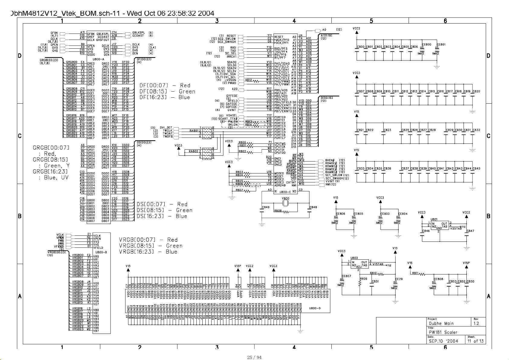
DbhM4812V12 Vtek BOM.sch-11 - Wed Oct 06 23:58:32 2004
GFBK i
[6,7] 1
GCLK i
[6,7,8] 1
[7,8] GPEN I
[6.7.8] GVS
[6.7.8] GHS
GRGB[00:23]
[6,7,B]
. GRGB01
. GRGR07 M
. GRGB03 h 4
. GRGBÛ4 U2
. GRGB05 U
. GRGB06 DA
. GRGB07 \)V
. GRGB08 C11
. GRGBÛ9Ü12
. GRGB10 Hl 1
. GRGB11 AH
. GRGB12 HK
. GRGB13 V.H
. GRGB14 A/
. GRGB15 H/
. GRGB16 R1R
. GRGB17A/’t)
. GRGB18 Hl/
. GRGB19 A19
. GRGB20Hl K
. GRGB21A1 /
. GRGB22
. GRGB23A1 b
GRGB[00:07]
: Red,
GRGB[08:15]
: Green, Y
GRGB[16:23]
: Blue, UV
VCLK
vrcs
VW3
vm
VFIBCD
_tai
VRGB[00:23]
[10]
GRGBQO E4
CA
A1h
C15
B15
A14
B14
A13
C12
B13
A12
VRGBOO E2
. VRGB01
. VRGB02
. VRGB03
. VRGB04
. VRGB05 HA
. VRGB06 HV
. VRGB07
. VRGB08
. VRGB09
. VRGB10 JA
. VRGB11
. VRGB12
. VRGB13 KA
. VRGB14 KV
. VRGB15 Kl
. VRGB6 1 ?
. VRGB/ 1 1
. VRGBHI A
. VRGB9 L4
. VRGB2DMA
. VRGB21 M1
. VRGB22
. VRGB23 M2
GFBKGBLKSPL
GREFGCOAST
GCLKGHSFOUT
GPEN DCLK
(WS
DVS
GHS DHS
USOG DEN
U800-A
GREO DREO
GRM DREI
GRE2 DRE2
GRE3 DRE3
GRE4 DRE4
GRE5 DRE5
GRE6 DRE6
GRE7 DRE7
GGEO DGEO
GGE1 DGE1
GGE2 DGE2
GGE3 DGE3
GGE4 DGE4
GGE5 DGE5
GGE6 DGE6
GGE7 DGE7
GBEO DBEO
GBE1 DBE1
GBE2 DBE2
GBE3 DBE3
GBE4 DBE4
GBE5 DBE5
GBE6 DBE6
GBE7 DBE7
GROO DROO
GR01 DR01
GR02 DR02
GROA
DR03
GR04 DR04
GR05 DR05
GR06 DR06
GR07 DR07
GGOO DGOO
GG01 DG01
GG02 DG02
GG03 DG03
GG04 DG04
GG05 DG05
GG06 DG06
GG07 DG07
GBOO DBOO
GB01 DB01
GB02 DB02
GB03 DB03
GH04 DB04
GB05 DB05
GB06 DB06
GB07 DB07
VCLK
VPEN
WS
VHS
VFIELD
VRO
H
VR1
\'i
VR2
UA
VR3
li?
VR4
VR5
VR6
1,1
VR7
,14
VGO
Hl
VG1
VG2
Ji»
VG3
J1
VG4
VG5
VG6
VG7
VBO
VB1
VB2
VB3
VB4
VB5
NI
VB6
VB7
A18 I—< GCOAST [6]
Y20 DFD1
R16 DF02
U19 DFD3
RIB
W20 DFD5
V20 DFD6
U20 DFD7
T19 DF08
T2Q DFD9
R19 DF1D
R20 DF11
M18 DF12
P18 DF13
P19 DF14
P20 DF15
M17 DF16
N20 DF17
M20 DF18
L17 DF19
M19 DF20
K17 DF21
L19 DF22
L20 DF23
K19 DSOO
K20 DS01
K1B DS02
J20 DS03
J18 DS04
J19 DS05
H20 DS06
H19 DS07
H18 DSOB
H17 DS09
G20 DS10
G19 DS11
G18 DS12
F20 DS13
F19 DS14
F18 DS15
E20 DS16
E19 DS17
E18 DS18
F17 DS19
D20 DS2D
D19 DS21
D16 DS22
D17 DS23
GBLKSPL [6]
[3,4]
[4]
[4]
DF[00:23]
[4] [6,8,12]
,
,
DF04
,
,
DF[00:07]
,
DF[08:15]
,
,
DF[16:23]
,
,
,
,
,
,
,
,
[5] DVI_DET
,
,
,
,
,
,
,
,
,
,
,
,
,
,
,
,
,
,
,
,
,
[3] TWCLK
[3] TWDAT
[3] TWDFB
DS[00:23]
[4]
DS[00:07]
DS[08:15]
DS[16:23]
[6,8,12]
Red
Sreen
Blue
Red
Green
Blue
VRGB[00:07] - Red
VRGB[08:15] - Green
VRGB[16:23] - Blue
V15
Á
io io ifs in io
9999q9o2S2d2Sd2c
¿Ü Ü ÛD Q ÜQ Û
-CNKWWtOr-OOO
Û ÛÛ Û Û Û QÛ Û Û Q ÛÛ Û Q ÛÛ Û Û ÛÛ Û Û ÛÛ Û Û ÛÛ Û Û ÛÛ Û Û ÛQ Û
z z z z z z z z z z z z z z z z z z z z z z z z z z z z z z z z z z z z z z
> > > > > > > > > '
MCMtMCNCMCNCMC'JC'
RESET
[12] SC2_SWL0W
[12] SC2_SWHIGH
Q Q Q Q
QÛ Û Q
>>>>
a œ i i
SMD|2 SMD 2
TTTTTTT
CBO7_[cB0bJcBO9_[cB1O_1cB11 _jcß12_]c 813_jcß14_}c B15_]c816_lc817_]cB1ß_lc819 Jcj
TTTTTTTTTTTTT
CB2ijçB22 jcB23 jçS25_lçB26_jçS27_[çBZe _jç829_jç83ojç831 jçj
TT T TTTT TTT
C B3^jcB3 ^jc B35_jc B36 jcß37_lc B3ßjcß39_[c B4 q_lcB41_[cB42_lcB43_[c844jcj
TTTT TTTTTTTT
VCC3
▲
OUT
,.|TAB
R.B10
Jç8!
1
)EB03 CE804
VCC3
A
L.
Project:
Dubhe Main
Title:
PW181 Scaler
Date: Sheet:
SEP.10 '2004 11 of 13
WB™
jçB53_jçB52 CI
11
VCC2
À
V15P
Á
Rev:
1.2
25/94
Page 29
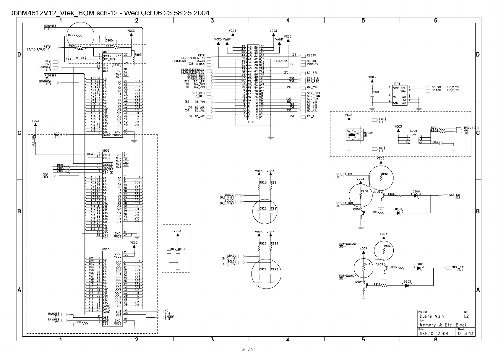
DbhM4812V12 Vtek BOM.sch-12 - Wed Oct 06 23:58:25 2004
RST# I
[3,7,8,9,10,12,13] 1—
-----
VCC3
A
VCC5 VAMP
>
RSTj
[3,7,8,9,10,12,13]
[6,8,11,12] SDA3G |
[2] REG5A I
[9,10,11,12BDA3V
[9,10,11,12]SCL3V
[13] SC1_B0X
[13] SC1_GRN
[12] SC1_SW
[9] MA_VIN
[9] MA_CIN
SC2_BLU I
SC2_RED
[5] S D_AIR I
[5] SD_AIL I
A A
SDA3G
[6,8,11,12]
SCL3G I
re b 11 ion 1--/
49
4/ 4H
4h
4 A44
41
AW41)
At
Ah
AAA4
A1
y 9
vt VH
Vh VH
VA
?1 VV
1«
1/ 1K
1h
1A 14
11 VV
9
/
h 6
A
1 2
-----
V
VCC3
50
46
4 y
AK
AH
AV
At)
V 4
VO
16
10
K
4
VCC3 VCC3
A
_<--1 REGBV
SCL3G
PWR33V
«
l SC1_BLU
I SC1_RED
] MA_YIN
SC2_B0X
SC2_GRN
SC2_SW
SB_V IN
SB_CIN
HD_AIR
HD_AIL
1 SCL3G [6,8,11,12]
SDA3G [6,8,11,12]
1 P C_AIL
R904 a « * I
-----
x IRRCVh [
SBi-pWLOW
SEi-pWHIGl
6
001 .
9
007 .
11)
003 .
13
D04 ,
14
005 .
15
D06 ,
IK 007 .
?9
D08 ,
Al>
009 .
31
D10 ,
AV
011 .
Ah
01? .
AH
013 .
At 014 .
AH
D15 >
39
40 h
1?
A4
1
-----
1
- 1
ptS:
Ï
ta
26/ 94
Se^SWLOW
SE^SWHIGI
Project:
Dubhe Main
Title:
Memory & Etc. Block
Date: Sheet:
Rev:
1.2
SEP.10 '2004 12 of 13
Page 30
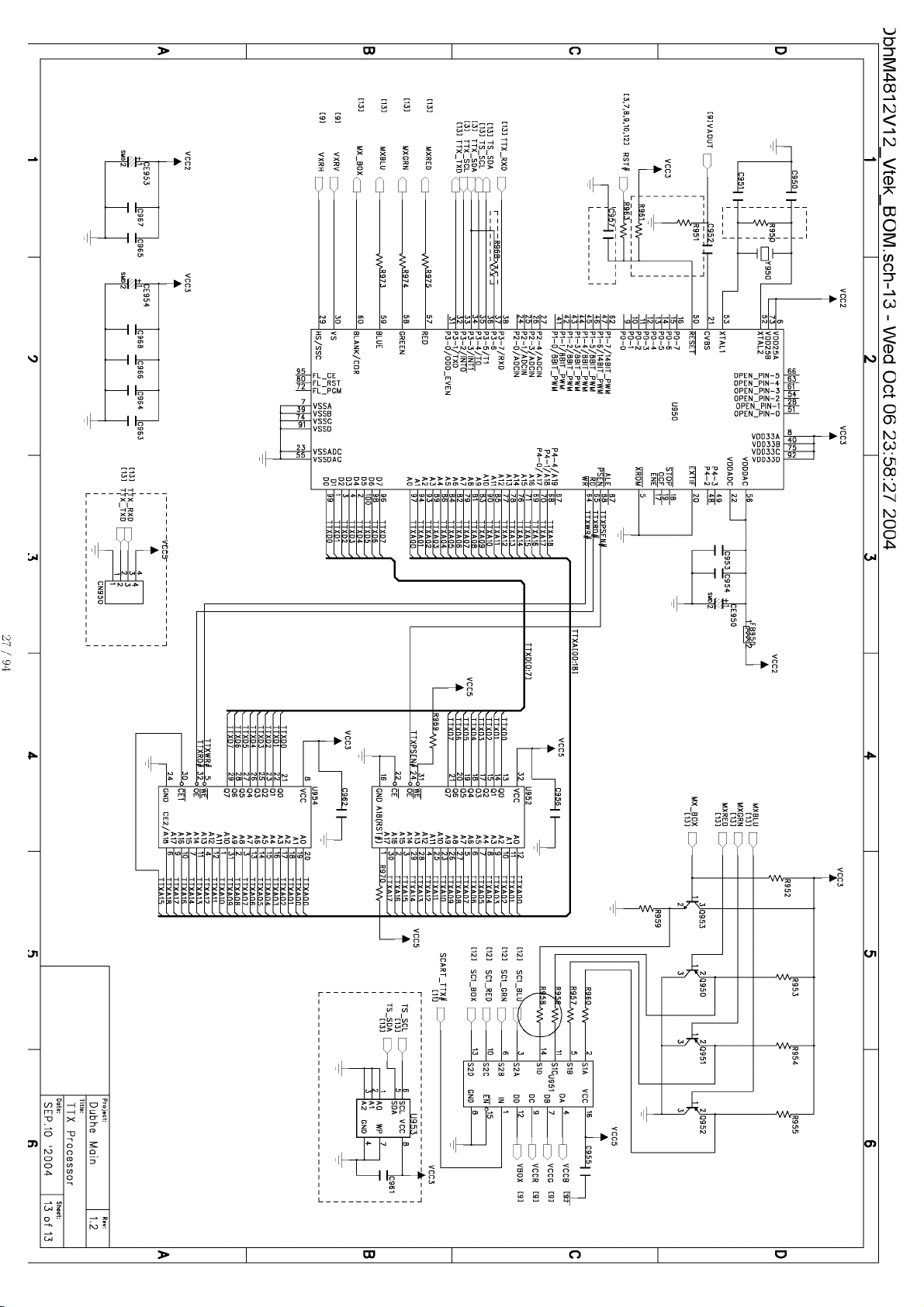
3bhM4812V12 Vtek BOM.sch-13 - Wed Oct 06 23:58:27 2004
27 /9 4
Page 31

Dbh1S4909V12.sch-2 - Thu Oct 07 00:30:42 2004
28/ 94
Page 32

Db h1S4909V 12.sch-3 - Thu Oct 07 00:30:43 2004
29/ 94
Page 33

Db h1S4909V 12.sch-4 - Thu Oct 07 00:30:45 2004
30/ 94
Page 34

Db h1S4909V 12.sch-5 - Thu Oct 07 00:30:47 2004
31/ 94
Page 35

Db h1S4909V 12.sch-6 - Thu Oct 07 00:30:49 2004
32/9 4
Page 36

Dbh1S4909V12.sch-7 - Thu Oct 07 00:30:50 2004
33/9 4
Page 37

Dbh2S4909V12.sch-2 - Thu Oct 07 00:32:34 2004
MAINSIF I-->_
n
AGC
TUNINGVCC
5V
SCL
SDA
AS TU
NC1
NC2
NC3
AS_IF
SIF
CVBS
GND1
GND2 5V IF
GND3
GND4 AF
H I-
■^BSOfr
^ ] S
Jc5io _c;
jf^&D I
VCC5
A
Rtûi^--! LR503
C506
I 501 ~.
C504
3505
Hh
C509 Ç5Q3
jOD ~
:
-S5!%r
Q5022
—<
VCC5
A
%
3
I—V TV1_VIN
^^ [2]
I—xSC1 VOUTSUB
“I—^ r?i
-o?
j_MT1
j_MT4
1 MT2
j_MT5
- b - Ö - f t - f t
|Oj
-fo]
SDA3V_TV I--y_
SDA3G_W I--v_
^<5-1
[2] s ^
SIF2 l_
[2] s--1
M0N0JN g—1__
TVI_VIN /--1
[2] ^--1
TV2_VIN /--1
[2] s--1
SC1_V0UTSUB
TUNER VCC
A"
TUNERVCC
VCC5
A
2-
IN OUT
INZGND™frti
'OATAfe
:E507
¥
SUD 2
TUNERVCC
Project:
Dubhe Sub
Title:
Tuner
Date: Sheet:
Sep. 9 '2004 02 of 02
Rev:
1.2
34/9 4
Page 38

DUBHE OSD Ver1.1 NAKS.sch-1 - Mon Oct 18 11:47:11 2004
3 5/ 94
Page 39

R702
56K
- w -
0025.sch-1 - Mon May 16 09:25:50 2005
REMOTE PCB
VD701
IN4148
X°“ l
O K51
yo-<>
X°~l
OK47
<?K48
^O—11
?K 4 4
✓o-hI
^K43
✓O—11
QK 36 g K 3 5
X°n
£ K 5 0
^O-i I
£K46
^Ohi
^K42
✓ O - o
£K38
^ O - o
gK34
✓ ° i
OK4 9
/'CH I
OK4 5
fO -ii
Q K41
^O—< I
OK37
^CHI
gK33
✓ ° 1
OK32
9K28
p/ O—< I
OK24
yo-<>
gK20
yo-f I
£k16
^ O - H
gK12
✓ O h >
gK8
^CH I
g K 4
0K31
yo->>
gK27
f O - o
~ K19
^ O H I
~K15
y ( X i
~>K11
yen I
>K7
^ O - o
g K3
^/O-i /'O-i
OK30 OK29
gK26
gK25
✓ C H »
^/Ohi
gK22
gK21
^ C H I
gK 1 8
£ K 1 7
yo~> >
gK 1 3
^CH I
gK10
«''Oh »
£ K 6
gK 5
✓CH I
^ / O h i
_gK2
g K1
»
aa.
22.
21
-2 ±
LL
J i .
J£.
JZ.
ja.
ja.
21
N701
PT2222
_ rv
XL.
€702
150pF
^t=TF"
□
G701 '¿7 0 3
455KHZ
a 150pF
B701
BT701
3V
H'l
C701
^7U/10V
+ 0 —
R701?701<
A°wf
V701
80 50
REMOTE CONTROL CODE ASSIGNMENT
KEY NO. KEY NAME DATA CODE KEY NO. KEY NAME DATA CODE
K1 POWER 00 K33 dumb 40
K2
K3 2 02 K35
K4
K5 P.M0DE 04 K37
K6
K7 5 06 K39 nil 46
K8
K9
K10 7 09 K42 PREV 49
K11 8 0A K43 P.STILL 4A
K12 9 0B K44 SOUND 4B
K13 MTS OC K45 SLEEP 4C
K14 nil 0D K46
K15
K16
K17
K18
K19
K20 C H.- 13 K52 nil 53
K21 MENU 14 K53 nil 54
K22
K23
K24
K25 0 18 K57 nil 58
K26
K27
K28 EXIT 1B K60 nil 5B
K29 PIP 1C K61 nil
K30
K31
K32 PIP CH+ 1F K64
1
3
4
6
nil
S.SELE
OK
CH.+
V0L.+
V0 L .-
Source
nil
P.SIZE
F.White
PIP Source
SWAP
PIP CH-
01 K34
03 K36 dumb 43
05 K38
07 K40 nil 47
08 K41 100 48
0E K47 Picture 4E
OF K48 CH Erase 4F
10 K49
11 K50 C/C 51
12 K51
15 K54 nil 55
16 K55 nil 56
17 K56
19 K58
1A K59 nil 5A
1D K62 nil 5D
1E K63 nil 5E
dumb
dumb
MUTE
INFO
TIME
CH Save
V-CHIP
nil
nil
nil
41
42
44
45
4D
50
52
57
59
5C
5F
CUSTOM CODE: 20DD
FOR NTSC
Page 40

Basic Operations & Circuit Description
MODULE
There are 1 pc. panel and 12 pc.s PCB including 2 pc.s Y/Z Sustainer board, 2 pc.s Y Drive
board, 6 pc.s X Extension boards, 1 pc. Control (Signal Input) and 1 pc. Power
board in the Module.
SET
There are 6 pc.s PCBs including 1 pc. AUX. PSU Board, 1 pc. Keypad board, 1 pc.
Remote Control Receiver board, 1 pc. L/R Speakers and 1 pc. Main (Video) board in the SET.
37/9 4
Page 41

Local Key
Stand Main (Video)
3 8/ 94
Tuner/Audio
X-extension Bottom L/C/R
Page 42

PCB function
1. Power:
(1). Input voltage: AC 110V~240V, 47Hz~63Hz.
Input range: AC 90V(Min)~265V(Max) auto regulation.
(2). To provide power for PCBs.
2. Main (Video InterFace) board: To converter TV signals, S signals, AV signals, Y Pb/
Cb Pr/Cr signals, DVI signals and D-SUB signals to digital ones and to transmit to
Control board.
3. Control board: Dealing with the digital signal for output to panel.
4. Y-Sustainer / Z-Sustainer board:
(1). Receiving the signals from Control and high voltage supply.
(2). Output scanning waveform for Module.
5. Y-Drive board: Receive signal from Y sustainer, output horizontal scanning wave
form to the panel.
6. X extension board (6pcs): Output addressing signals.
7. Tuner/Audio Board: Process and Amplifying the audio signal to speakers and
convert TV RF signal to video/audio signal and send to Main board.
39/9 4
Page 43

PCB failure analysis
1. CONTROL : a. Abnormal noise on screen. b. No picture.
2. MAIN (video) : a. Lacking color, Bad color scale.
b. No voice.
c. No picture but with signals output, OSD and back light.
d. Abnormal noise on screen.
3. POWER : No picture, no power output.
4. Z - Sustainer :a. No picture.
b. Color not enough.
c. Flash on screen.
5. Y - Sustainer : Darker picture with signals.
6. X - Extension : Abormal vertical noise on screen.
7. Audio Board or AUX PSU: a. No voice. (Make sure Mute/OFF) .
b. Noise.
4 0/ 94
Page 44

Basic operation of Plasma Display
1. After turning on power switch, power board sends 5Vst-by Volt to M icro Processor
2. The micro Processor m em orize the last state of Power, W hen the last state of
power is on or receive power on signal from local Key or Rem ote control, Micro
Processor will send on control signal to power. Then Power sends (5Vsc, 9Vsc,
24V and RLYON, Vs ON) to PCBs w orking. This time VIF will send signals to
display Image, OSD on the panel and start to search available signal sources.
If the audio signals input, them will be am plified by A udio AMP and transm itted to
Speakers.
3. If som e abnorm al signals are detected (for exam ple: over volts, over current, over
tem perature and under volts), the system will be shut down by Power off.
4 1/ 94
Page 45

Main IC Specifications
- PW181 Image Processor, Scaler
- PW1231 Digital Video Signal Processor
- uPD64083 Three -Dimensional Y/C Separation LSI
With On-Chip Memory
- AD9883A 110MSPS/140MSPS Analog Interface
- VPC 323XD Comb-filter Video Processor
- Si161B Panel Link Receiver
- Z86229 NTSC Line 21 CCD decorder
- MSP34x0G Multistandard Sound Processor
4 2/ 94
Page 46

P W181
Product Specification
General Description
The PW181 ImageProcessor is a highly integrated
“system-on-a-chip” that interfaces computer graphics and
video inputs in virtually any format to a fixed-frequency flat
panel display.
Computer and video images from NTSC/PAL to WUXGA
at virtually any refresh rate can be resized to fit on a fixed-
frequency target display device with any resolution up to
WUXGA. Video data from 4:3 aspect ratio NTSC or PAL
and 16:9 aspect ratio HDTV or SDTV is supported. Multi
region, nonlinear scaling allows these inputs to be resized
optimally for the native resolution of the display.
Advanced scaling techniques are supported, such as
format conversion using multiple programmable regions.
Three independent image scalers coupled with frame
locking circuitry and dual programmable color lookup
tables create sharp images in multiple windows, without
user intervention.
Embedded SDRAM frame buffers and memory controllers
perform frame rate conversion and enhanced video
processing completely on-chip. A separate memory is
dedicated to storage of on-screen display images and
CPU general purpose use.
Advanced video processing techniques are supported
using the internal frame buffer, including motion adaptive,
temporal deinterlacing with film mode detection. When
used in combination with the new third-generation scaler,
this advanced video processing technology delivers the
highest quality video for advanced displays.
Both input ports support integrated DVI 1.0 content
protection using standard DVI receivers.
A new advanced OSD Generator with more colors and
larger sizes supports more demanding OSD applications,
such as on-screen programming guides. When coupled
with the new, faster, integrated microprocessor, this OSD
Generator supports advanced OSD animation techniques.
Video
TV
Signal
TV
Signal
Input
TV Tuner
Com puter
Com puter
j TV Tuner j
Video
Input
Video
Decoder
ADC/
TMDS
ADC/
TMDS
r 1
Video
Decoder
PW181 System Block Diagram
Crystal
~ r
PW181
ROM
Features
• Third-generation, two-dimensional filtering techniques
• Third-generation, advanced scaling techniques
• Second-generation Automatic Image Optim ization
• Fram e rate conversion
• Video processing
• On-Screen Display (OSD)
• On-chip microprocessor
• JTAG debugger and boundary scan
• Picture-in-picture (PIP)
• Multi-region, non-linear scaling
• Hardware 2-wire serial bus support
Applications
• Multim edia Displays
• Plasma Displays
• Digital Television
Device Application Package
PW181-10V Up to XGA Displays
PW181-20V Up to UXGA Displays
352 PBGA
Dis p lay
Programmable features include the user interface, custom
start-up screen, all automatic imaging features, and
special screen effects.
p ix e lw o r k s
8100 SW Nyberg Road
Tualatin, OR 97062 USA
Telephone: 503.454.1750
FAX: 503.612.0848
www.pixelworks.com PRELIMINARY I CONFIDENTIAL
43/94
Page 47

ANALO G 110 MSPS/140 MSPS Analog Interface
►
FEATURES
140 MSPS Maximum Conversion Rate
300 MHz Analog Bandwidth
0.5 V to 1.0 V Analog Input Range
500 ps p-p PLL Clock Jitter at 110 MSPS
3.3 V Power Supply
Full Sync Processing
Sync Detect for “Hot Plugging”
Midscale Clamping
Power-Down Mode
Low Power: 500 mW Typical
4:2:2 Output Format Mode
APPLICATIONS
RGB Graphics Processing
LCD Monitors and Projectors
Plasma Display Panels
Scan Converters
Microdisplays
Digital TV
DEVIC ES for Flat Panel Displays
AD9883A
FUNC TIO NA L BLOCK D IAG RAM
GENERAL DES CRIPTION
The AD9883A is a complete 8-bit, 140 MSPS monolithic analog
interface optimized for capturing RGB graphics signals from
personal computers and workstations. Its 140 M SPS encode
rate capability and full power analog bandwidth of 300 MHz
supports resolutions up to SXGA (1280 x 1024 at 75 Hz).
The AD 9883A includes a 140 MHz triple AD C with internal
1.25 V reference, a PLL, and programmable gain, offset, and
clamp control. The user provides only a 3.3 V power supply,
analog input, and Hsync and COA ST signals. Three-state
CMOS outputs may be powered from 2.5 V to 3.3 V.
The A D9883A’s on-chip PLL generates a pixel clock from the
Hsync input. Pixel clock output frequencies range from 12 MHz to
140 MHz. PLL clock jitter is 500 ps p-p typical at 140 M SPS.
When the COAST signal is presented, the PLL maintains its
output frequency in the absence of Hsync. A sampling phase
adjustment is provided. Data, Hsync, and clock output phase
relationships are maintained. The AD9883A also offers full sync
processing for composite sync and sync-on-green applications.
A clamp signal is generated internally or may be provided by
the user through the CLAMP input pin. This interface is fully
programmable via a 2-wire serial interface.
Fabricated in an advanced CMOS process, the AD9883A is
provided in a space-saving 80-lead LQ FP surface-mount plastic
package and is specified over the 0°C to 70°C temperature range.
REV. A
Information furnished by Analog Devices is believed to be accurate and
reliable. However, no responsibility is assumed by Analog Devices for its
use, nor for any infringements of patents or other rights of third parties that
may result from its use. No license is granted by implication or otherwise
under any patent or patent rights of Analog Devices.
4 4/ 94
One Technology Way, P.O. Box 9106, Norwood, MA 02062-9106, U.S.A.
Tel:
Fax:
Page 48

PW1231A
Product Specification
General
The PW1231A is a high-quality, digital video signal
processor that incorporates Pixelworks' patented
deinterlacing, scaling, and video enhancement
algorithms. The PW1231A accepts industry-standard
video formats and resolutions, and converts the input into
many desired output formats.The highly efficient video
algorithms result in excellent quality video.
The PW1231A combines many functions into a single
device, including a memory controller, auto-configuration,
and others. This high level of integration enables simple,
flexible, cost-effective solutions that require fewer
components.
Crystal
Video
PW1231A
System Block Diagram
Video
Decoder
PW1231A
PW1231AL
SD RAM
Digital
Output
Features
• Built-In Memory Controller
• Motion-Adaptive Deinterlace Processor
• Intelligent Edge Deinterlacing
• Digital Color/Luminance Transient Improvement (DCTI/DLTI)
• Interlaced Video Input Options, including NTSC and PAL
• Independent horizontal and vertical scaling
• Copy Protection
• Two-Wire Serial Interface
Applications:
For use with Digital Displays
• Flat-Panel (LCD, DLP) TVs
• Rear Projection TVs
• Plasma Displays
• LCD Multimedia Monitors
• Multimedia Projectors
Device Application Package
PW1231A
PW1231AL
NOTE: “L” denotes lead (Pb) free
Up to XGA 160-pin PQF
p ix e lw o r k s
8100 SW Nyberg Road
Tualatin, OR 97062 USA P/N 001-0097-00 Rev B
Telephone: 503.612.6700 July 2003
PRELIMINARY-CONFIDENTIAL
4 5/ 94
Page 49

DATA SHEET
MOS INTEGRATED CIRCUIT
N E C
THREE-DIMENSIONAL Y/C SEPARATION LSI WITH ON-CHIP MEMORY
DESCRIPTION
The ^PD 64083 realizes a high precision Y/C separation and a noise reduction by the three-dimension signal
processing for NTSC signal.
This product has the On-chip 4-Mbit m emory for flame delay, 2ch of high precision internal 10-bit A/D converter, and
adapting 10-bit signal processing (only for luminance signal) and high picture quality. The ^PD 64083 is completely
single-chip system of 3D Y/C separation.
This LSI includes the Wide Clear Vision ID signal (Japanese local format) decoder and ID-1 signal decoder.
FEATURES
• On-chip 4-Mbit frame delay memory.
• 4 Operation mode (Compatible to the ^PD 64082)
Motion adaptive 3D Y/C separation (for Composite video input)
Frame recursive Y/C NR (for Y/C separated video input)
Frame comb type YNR + 1H delayed C signal (for Y/C separated video input)
2D Y/C separation + Frame recursive Y/C NR (for Composite video input)
• Em bedded A/D converter (2ch), D/A converter (2ch), clock generator.
• Em bedded Y coring, Vertical enhancer, Peaking filter, and Noise detector.
• Em bedded W CV-ID decoder and ID-1 decoder.
• I2C bus control.
• Dual power supply of 2.5 V and 3.3 V.
For digital : DVdd = 2.5 V
For analog : AVdd = 2.5 V
For DRAM : DVddram = 2.5 V
For I/O : DVddio = 3.3 V
ORDERING INFORMATION
Part number
JuPD64083G F-3BA
100-pin plastic QFP (14 x 20)
Package
Document No. S15849EJ1V0DS00 (1st edition)
Date Published January 2002 NS CP (K)
Printed in Japan
4 6/ 94
Page 50

PRELIMINARY DATA SHEET VPC 323xD
Com b F ilter Video Proc esso r
1. Intro duction
The VPC 323xD is a high-quality, single-chip video
front-end, which is targeted for 4:3 and 16:9, 50/60-Hz
and 100/120 Hz TV sets. It can be combined with other
members of the DIGIT3000 IC family (such as
DDP 331x) and/or it can be used with 3rd-party prod
ucts.
The main features of the VPC 323xD are
- high-performance adaptive 4H comb filter Y/C sepa
rator with adjustable vertical peaking
- multi-standard color decoder PAL/NTSC/SECAM
including all substandards
- four CVBS, one S-VHS input, one CVBS output
- two RGB/YCrCb component inputs, one Fast Blank
(FB) input
- integrated high-quality A/D converters and associ
ated clamp and AGC circuits
- multi-standard sync processing
- linear horizontal scaling (0.25 ... 4), as well as
non-linear horizontal scaling ‘Panoramavision'
- PAL+ preprocessing
- peaking, contrast, brightness, color saturation and
tint for RGB/YCrCb and CVBS/S-VHS
- high-quality soft mixer controlled by Fast Blank
- PIP processing for four picture sizes (1-, 1-,
36 of normal size) with 8 -bit resolution
1 6 , or
- 15 predefined PIP display configurations and expert
mode (fully programmable)
- control interface for external field memory
- I2 C-bus interface
- one 20.25-MHz crystal, few external components
- 80-pin PQFP package
1.1. System A rch itecture
Fig.1-1 shows the block diagram of the video proces
sor
- line-locked clock, data and sync, or 656-output
interface
c i n o
VIN1 O
VIN20
VIN30
VIN40-
VOUTO
RGB/
YCrCb
FBO
RGB/q -
YCrCb
Y OUT
LL Cock
H Sync
V Sync
AVO
Fig. 1-1 : Block diagram of the VPC 323xD
Micronas
HDH
20.25 MHz I2C Bus
47/94
Page 51

Sil 161B PanelLink® Receiver
Data Sheet
August 2002
Gen eral D escrip tion
The SiI 161B receiver uses PanelLink Digital
technology to support high-resolution displays up to
UXGA (25-165MHz). This receiver supports up to true
color panels (24 bits per pixel, 16M colors) with both
one and two pixels per clock.
All PanelLink products are designed on a scaleable
CMOS architecture, ensuring support for future
performance enhancements while maintaining the
same logical interface. System designers can be
assured that the interface will be stable through a
number of technology and performance generations.
PanelLink Digital technology simplifies PC and display
interface design by resolving many of the system level
issues associated with high-speed mixed signal design,
providing the system designer with a digital interface
solution that is quicker to market and lower in cost.
Features
Low Power Operation: 280mA max. current
consumption at 3.3V core operation
Time staggered data output for reduced ground
bounce and lower EMI
Sync Detect feature for Plug & Display
Cable Distance Support: over 5m with twisted
pair, fiber-optics ready
ESD tolerant to 5kV (HBM on all pins)
Compliant with DVI 1.0 (DVI is backwards
compatible with VESA® P&DTM, FPDI-2™ and
DFP)
HSYNC de-jitter circuitry enables stable operation
even when HSYNC contains jitter
Low power standby mode
Automatic entry into standby mode with clock
detect circuitry
Standard and Pb-free packages (see page 25).
4 8/ 94
Page 52

O
Pr e l im in a r y Pr o d u c t Sp e c if ic a t io n
o
Z86229
N
Totally Logical
FEATURES
Speed Pin C ount/ Standard On-Screen Display Program
Devices (M H z) Package Types Tem p . Range & Closed Captioning Rating T im e of Day
Z86229 V 2 18-Pin DIP, SOIC 0°C to +70°C Yes Yes Yes
NTSC Line 21 CCD Decoder
Autom atic Data Extraction
Complete Stand-Alone Line 21 Decoder for Closed-
Captioned and Extended Data Services (XDS)
Preprogrammed to Provide Full Compliance with
EIA-608 Specifications for Extended Data Services
Automatic Extraction and Serial Output of Special
XDS Packets (Time of Day, Local Time Zone, and
Program Blocking)
Programmable XDS Filter for a Specific XDS Packet
Cost-Effective Solution for NTSC Violence Blocking
inside Picture-in-Picture (PiP) Windows
GENERAL DESCRIPTION
Capable of processing Vertical Blanking Interval (VBI)
data from both fields of the video frame in data, the Z86229
Line 21 Decoder offers a feature-rich solution for any tele
vision or set-top application. The robust nature of the
Z86229 helps the device conform to the transmission format
defined in the Television Decoder Circuits Act of 1990, and
in accordance with the Electronics Industry Association
specification 608 (EIA-608).
The Line 21 data stream can consist of data from several data
channels multiplexed together. Field 1 consists of four data
channels: two Captions and two Texts. Field 2 consists of
five additional data channels: two Captions, two Texts, and
Extended Data Services (XDS). The XDS data structure is
Minimal Communications and Control Overhead Pro
vide Simple Implementation of Violence Blocking,
Closed Captioning, and Auto Clock Set Features
Programmable, On-Screen Display (OSD) for Creat
ing Full Screen OSD or Captions inside a Picture-in-
Picture (PiP) Window
User-Programmable Horizontal Display Position for
easy OSD Centering and Adjustment
I2C Serial Data and Control Communication
Supports 2 Selectable I C Addresses
defined in EIA-608. The Z86229 can recover and display
data transmitted on any of these nine data channels.
The Z86229 can recover and output to a host processor via
the I2C serial bus. The recovered XDS data packet is further
defined in the EIA-608 specification. The on-chip XDS fil
ters in the Z86229 are fully programmable, enabling recov
ery of only those XDS datapackets selected by the user. This
functionality allows the device to extract the required XDS
information with proper XDS filter setup for compatibility
in a variety of TVs, VCRs, and Set-Top boxes.
In addition, the Z86229 is ideally suited to monitor Line 21
video displayed in a PiP window for violence blocking,
CCD, and other XDS data services. A block diagram of the
Z86229 is illustrated in Figure 1.
D S 00 51 0 3 - 0 6 0 1
49/94
Page 53

PRELIMINARY DATA SHEET
MSP 34xOG
Multistandard Sound P rocessor Family
Release Note: R evision bars indicate significant
changes to the previous edition. The hardware and
software description in this document is valid for
the MSP 34xOG version B8 and following version s.
1. Introduction
The MSP 34xOG family of single-chip Multistandard
Sound Processors covers the sound processing of all
analog TV-Standards worldwide, as well as the NICAM
digital sound standards. The full TV sound processing,
starting with analog sound IF signal-in, down to pro
cessed analog AF-out, is performed on a single chip.
Figure 1-1 shows a simplified functional block diagram
of the MSP 34xOG.
This new generation of TV sound processing ICs now
includes versions for processing the multichannel tele
vision sound (MTS) signal conforming to the standard
recommended by the Broadcast Television Systems
Committee (BTSC). The DBX noise reduction, or alter
natively, Micronas Noise Reduction (MNR) is per
formed alignment free.
Other processed standards are the Japanese FM-FM
multiplex standard (EIA-J) and the FM Stereo Radio
standard.
Current ICs have to perform adjustment procedures in
order to achieve good stereo separation for BTSC and
EIA-J. The MSP 34xOG has optimum stereo perfor
mance without any adjustments.
All MSP 34xxG versions are pin compatible to the
MSP 34xxD. Only minor modifications are necessary
to adapt a MSP 34xxD controlling software to the
MSP 34xxG. The MSP 34xOG further simplifies con
trolling software. Standard selection requires a single
l2C transmission only.
The MSP 34xOG has built-in automatic functions: The
IC is able to detect the actual sound standard automat
ically (Automatic Standard Detection). Furthermore,
pilot levels and identification signals can be evaluated
internally with subsequent switching between mono/
stereo/bilingual; no l2C interaction is necessary (Auto
matic Sound Selection).
The MSP 34xOG can handle very high FM deviations
even in conjunction with NICAM processing. This is
especially important for the introduction of NICAM in
China.
The ICs are produced in submicron CMOS technology.
The MSP 34xOG is available in the following packages:
PLCC68 (not intended for new design), PSDIP64,
PSDIP52, PQFP80, and PLQFP64.
Sound IF1 o-
Sound IF2 &
SCART3
SCART4
MONO »
Fig. 1 -1 : Simplified functional block diagram of the MSP 34xOG
Loud
speaker
Sound
Processing
Headphone
Sound
Processing
DAC
DAC
DAC
DAC
SCART
Output
Select
Loud
C
speaker
«0 Subwoofer
Headphone
SCART1
c
SCART2
c
Micronas
Page 54

MODEL : SG" HD D3.1 PDP
1,269cm (50 Inch) Wide Plasma Display Module
Quality innovation Team
5 1/ 94
Page 55

CONTENTS
1.O v e rv iew
1-1 Model Name of plasma Display
1-2 External View
1-3 Specifications
2. P re ca utio n
2-1 Handling Precaution for Plasna Display,
2-2 Safety Precautions for Service (Handling, prevention of a electrical shock, measure against
power outage, etc)
3. N am e & F un ction
3-1 Layout of Assemblies
3-2 Block Diagram:
3-3 Main function of Each Assembly
3-4 Product/Serial Label Location
4. O p er ation ch e ckin g a fter rectifica tion
4-1 Flow chart
4-2 Defects , Symptoms and Detective Parts
5. D isa s se m b lin g / A s se m b ling
5-1 Tools and measurement equipment
5-2 Exploded View
5-3 Disassembling & Re-assembling
6. O p era tion C h e c k a fter R ep air Ser v ice
6-1 Check Item
6-2 Check Procedure
5 2/ 94
Page 56

__
Formation and Specification of Module
^ 1'k * /v i» » am ^ \ • /
. Over vi ew
1
1-1 Model Name of Plasma Display
MODEL : 50HD” D3.1 P DP (S50HW-XD03)
1-2 External View
[ M3 = X Board + Y Board + Logic Board + PSU + SUB PSU ]
5 3/ 94
Page 57

1-3 Points of Screw Mount
Trouble Shooting
Blue Dot : SC R E W 4X 12
Red Dot : SC R E W 3X10
5 4/ 94
Page 58

1-4 Specifications
No Item S p ec ifica tio n
1 Pixel
Horizontal 1366 X Vertical 768 pixels
(1 pixel = 1 R,G,B cells)
2 Number of Cells
3 Pixel Pitch
4
Cell Pitch
5 Display size
R
G
B
Horizontal 4,098 X Vertical 768 cells
Horizontal 810m X Vertical 810m
Horizontal 270m X Vertical 810m
Horizontal 270m X Vertical 810m
Horizontal 270m X Vertical 810m
Horizontal 1106.46m X Vertical 622.08m
6 Screen size Diagonal 50" Color Plasma Display Module
7 Screen aspect 16 : 9
8 Display color 16.77 million colors
Over 160°
9 Viewing angle
(Angle with 50% and greater brightness perpendicular to PDP
module)
10 Dimensions
1184(W) x 700 (H) x 60.1 (D) m
11 Weight Module 1 About 18.0 kg
12 Packing weight Module 1
13 Packing size
L 760 * W 1465 * H 1106(mm) / 10pcs/BOX
140kg ± 5kg (including modules) /
5pcs/BOX
60Hz/ 50Hz, LVDS
Broadcasting reception
14
Vertical frequency
and
Video/Logic Interface
5 5/ 94
Page 59

Samsung SDI Co. Ltd
2 . P r e c a u t io n
A/S Manual Plasna Dispày Mot
** T o p re ven t th e risk s of unit d a m age , ele ctrical s h o c k a nd radiation, ta ke th e
follo w in g sa fe ty , se r v ice, an d ESD p re ca u tion s .
2-1 Handling Precautions for Plasm a Display
PDP module use high voltage that is
dangerous to human. Before operating
PDP, always check the dust to prevent
circuit short. Be careful touching the
circuit device when power is on.
PDP module is sensitive to dust and
humidity. Therefore, assembling and
disassembling must be done in no dust
place.
PDP module has a lot of electric
devices. Service engineer must wear
equipment(for example , earth ring) to
prevent electric shock and working
clothes to prevent electrostatic.
■ PDP module use a fine pitch connector
which is only working by exactly
connecting with flat cable. Operator
must pay attention to a complete
connection when connector is
reconnected after repairing.
■ The capacitor's remaining voltage in
the PDP module's circuit board
temporarily remains after power is off.
Operator must wait for discharging of
remaining voltage during at least 1
minute.
2-2 Safety Precautions for Service (Handling, prevention o f a electrical shock , m easure
against pow er ou tage, etc)
( Safety Precautions )
Before replacing a board, discharge forcibly
The remaining electricity from board.
When connecting FFC and TCPs to the
module, recheck that they are perfectly
connected.
■ To prevent the Logic circuit from being
damaged due to wrong working, do not
connect/disconnect signal cables during
circuit operations.
To prevent electrical shock, be careful not
to touch leads during circuit operations.
5 6/ 94
Page 60

le
■ Do thoroughly adjustment of a voltage label
and voltage-insulation.
■ Before reinstalling the chassis and the
chassis assembly, be sure to use all
protective stuffs including a nonmetal
controlling handle and the covering of
partitioning type.
■ Caution for design change : Do not install
any additional devices to the module, and
do not change the electrical circuit design.
■ For example: Do not insert a subsidiary
audio or video connector. If you insert It, It
cause danger on safety. And, If you change
the design or insert, Manufactor guarantee
■ Examine carefully the cable status if it is
twisted or damaged or displaced. Do not
change the space between parts and circuit
board. Check the cord of AC power
preparing damage.
■ Product Safety Mark : Some of electric or
implement material have special
characteristics invisible that was related on
safety. In case of the parts are changed
with new one, even though the Voltage and
Watt is higher than before, the Safety and
Protection function will be lost.
■ The AC power always should be turned off,
before next repair..
will be not effect. .
■ Check assembly condition of screw, parts
and wire arrangement after repairing.
■ If any parts of wire is overheats of damaged,
replace it with a new specified one
Check whether the material around the
parts get damaged.
immediately, and identify the cause of the
problem and remove the possible
dangerous factors.
( Precaution w hen repairing ESD )
■ There is ESD which is easily damaged by electric by ground connection, or must wear
electrostatics.(for example Integrated circuit, the antistatic wrist-belt and ring. ( It must be
FET ) Electrostatic damage rate of product operated after removing dust on it - It
will be reduced by the following technics comes under precaution of electric shock.)
■ Before handling semiconductor
parts/assembly, must remove positive
5 7/ 94
Page 61

Samsung SDI Co. Ltd. A/S Manual Plasma Display Mo
After removing ESD assembly, put on it with
aluminum stuff on the conductive surface to
prevent charging.
Do not use chemical stuff using Freon. It
generates positive electric that can damage
ESD.
Must use a soldering device for ground-tip
when soldering or de-soldering ESD.
Must use anti-static solder removal device.
Most removal device do not have antistatic
which can charge a enough positive electric
enough damaging ESD.
Before removeing the protective material
protective material into contact with the
chassis or assembly that the ESD is to be
installed on.
■ When handing an unpacked ESD for
replacement, do not move around too much
Moving (legs on the carpet, for example)
generates enough electrostatic to damage
the ESD.
■ Do not take a new ESD from the protective
case until the ESD is ready to be installed.
Most ESD have a lead, which is easily
short-circuited by conductive materials
(such as conductive foam and aluminum)
from the lead of a new ESD, bring the
5 8/ 94
Page 62

5 9/ 94
Page 63

No. Code No. Location Name
1 LJ44-00065A Main PUS ASSY PCB PSU
2 LJ44-00099A SUB-PSU ASSY PCB SUB-PSU
3 LJ92-00949C LOGIC-MAIN Board ASSY PCB LOGIC MAIN
4 LJ92-00852A X-MAIN Driving Board ASSY PCB X MAIN
5 LJ92-00853A Y-MAIN Driving Board ASSY PCBY MAIN
6 LJ92-00917A LOGIC E BUFFER Board ASSY PCB BUFFER
7 LJ92-00918A LOGIC F BUFFER Board ASSY PCB BUFFER
8 LJ92-00919A LOGIC G BUFFER Board ASSY PCB BUFFER
9 LJ92-00920A LOGIC H BUFFER Board ASSY PCB BUFFER
10 LJ92-00921A LOGIC I BUFFER Board ASSY PCB BUFFER
11 LJ92-00922A LOGIC J BUFFER Board ASSY PCB BUFFER
12 LJ92-00880A Y-BUFFER (UPPER) Board ASSY PCB BUFFER
13 LJ92-00881A Y-BUFFER (DOWN) Board ASSY PCB BUFFER
14 LJ92-00959A SUB-R ASSY PCB BUFFER
15 LJ92-00923A SUB-L ASSY PCB BUFFER
16
17
18
19
20
21
22
23
24
25
26
27
28
29
30
31
3809-001526
3809-001516
3809-001414
3809-001414
3809-001414
3809-001415
3809-001415
3809-001415
LJ39-00121A
LJ39-00121A
LJ39-00121A
LJ39-00121A
LJ39-00122A
LJ39-00122A
LJ39-00113A
LJ39-00118A
LOGIC + Y-MAIN FFC CABLE-FLAT
LOGIC + X-MAIN FFC CABLE-FLAT
SUB R + LOGIC FFC CABLE-FLAT
SUB L + LOGIC FFC CABLE-FLAT
LOGIC BUF(I) + LOGIC BUF(J) (UP) FFC CABLE-FLAT
LOGIC + LOGIC BUF(E)(Down) FFC CABLE-FLAT
LOGIC + LOGIC BUF(F)(Down) FFC CABLE-FLAT
LOGIC + LOGIC BUF(G)(Down) FFC CABLE-FLAT
LOGIC BUF(E) + LOGIC BUF(F) LEAD CONNECTOR
LOGIC BUF(F) + LOGIC BUF(G) LEAD CONNECTOR
LOGIC BUF(H) + LOGIC BUF(I) LEAD CONNECTOR
LOGIC BUF(I) + LOGIC BUF(J) LEAD CONNECTOR
Y-MAIN + LOGIC BUF(H) LEAD CONNECTOR
Y-MAIN + LOGIC BUF(E) LEAD CONNECTOR
PSU + LOGIC MAIN LEAD CONNECTOR
PSU + LOGIC BUF(E) LEAD CONNECTOR
32
33
34
35
LJ39-00177A
LJ39-00175A
LJ39-00173A
LJ39-00178A
PSU + LOGIC BUF(H) LEAD CONNECTOR
PSU + Y-MAIN LEAD CONNECTOR
PSU + X-MAIN LEAD CONNECTOR
PSU + SUB PSU LEAD CONNECTOR
6 0/ 94
Page 64

1. L-Main 2.X-Main
6 1/ 94
Page 65

9. J-Buffer 10. Y-Buffer (lower)
3-2 BLOCK DIAGRAM
3-2-1 BLOCK DIAGRAM FOR DRIVE CIRCUIT OPERATION
6 2/ 94
Page 66

To be Updated
3-2-2 Block Diagram for Logic circuit Block Diagram
DATA_R
a(9)Bits
DATA_G
a(9)Bits
DATA B
X Pulse
Vb
Reference
-Vcc Vo lta g e f o r L ogic C o ntro l
-V dd
-Va Vo lta g e fo r a ddress pu lse
-Vsc _l
-V scan V olta g e f o r sc an h ig h
-Vb Vo lta g e fo r X b ia s
-V se t
V o ltag e fo r FET d riv e r
V o ltag e fo r s u s ta in low
V o ltag e fo r Y ramp p u ls e
3-3 Main function o f Each A ssem b ly
■ X-main board : The X-main board generate a drive signal by switching the FET in synchronization with logic
main board timing and supplies the X electrode of the panel with the drive signal through the
connector.
1) Maintain voltage waveforms (including ERC)
2) Generate X rising ramp signal
3) Maintain Ve bias between Scan intervals
■.Y -main board : The Y-main board generate a drive signal by switching the FET in synchronization with the logic
Main Board timing and sequentially supplies the Y electrode of the panel with the drive signal
through the scan driver IC on the Y-buffer board. This board connected to the panel's
Y terminal has the following main functions.
1) Maintain voltage waveforms (including ERC)
6 3/ 94
Page 67

2) Generate Y-rising Falling Ramp
3) Maintain V scan bias
■ Logic main board : The logic main board generates and outputs the address drive output signal and the X ,Y
drive signal by processing the video signals. This Board buffers the address dirve output
signal and feeds it to the address drive IC (COF module)
(video signal- X Y drive signal generation , frame memory circuit / address data rearrangement)
■.Logic buffer(E,F) : The logic buffer transmits data signal and control signal.
■.Y-buffer board (Upper, Lower) : The Y-buffer board consisting of the upper and lower boards supplies the
Y-terminal with scan waveforms. The board comprises 8 scan driver IC's
(ST microelectronics STV 7617 : 64 or 65 output pins) , but 4 ICs for the SD class
■.AC Noise Filter : The AC Noise filter has function for removing noise(low Frequency) and blocking surge.
It effects Safety standards(EMC,EMI)
■.TCP( Tape Carrier Package ) : The TCP applies Va pulse to the address electrode and constitutes address
discharge by the potential difference between the Va pulse and the pulse
applied to the Y electrode. The TCP comprise 4 data driver Ics(STV7610A
:96 pins output pins) 7 TCPs are required for signal scan
6 4/ 94
Page 68

3-4 PRODUCT/ SERIAL LABEL LOCATION
Se rial No.
Voltage label
3-4-1 Serial No.
2 6 1 4 0 8 07 0 8 6 5
Serial No : 0001~9999
Date :
Month
1i1
T
01
CM
Year : 00(2000)
~99(2099)
Line No : 1 ~ 9
(0:Pilot Line)
Type : 02~48 ( e x . 5 0 H D v 3 :2 6 )
(Step of even)
6 5/ 94
Page 69

4 . O P E R A T I O N C H E C K IN G A F T E R R E C T IF IC A T IO N
4-1 Flow chart
* A/S Check Point *
1 .Checking the voltage for each assembly
L
j:
2. Judging the Logic board working or not [Vsync, 3.3 V, 5 V]
jd
3. Adjusting the output signal through test points
4. Checking the panel’s crack
4-1-1 No voltage output
OK
NG
NG
Reconnect it
PSU Voltage ch eck
D5V; 5V Check
Vs ; 170V Check
Va ; 72V Check
Vset; 18QV C heck
6 6/ 94
Vscan;-9QV Check
Vb; 155 V Check
Vcc; 1 5V Check
Vcan_h; 25V Check
D3V3; 3.3V Check
9Vstandby;9V Check
Fuse 8QQ1/8QQ2/8QQ3
—
Page 70

On/OFF Relay
(RLY 8001, 8002
Acts?
PSU
LED (Green) Replace
w
w
8001, 8002 off
PSU
6 7/ 94
OK
r
1
Go to 4-1-2 No Display
Page 71

4-1-2 NO display (operating Voltage but an image doesn’t exist on Screen)
=» No Display is related with Y-MAIN, X-MAIN, Logic Main and so on.
This page shows you how to check the boards, and the following pages show you how to find
the defective board.
N o D is p l a y
L o g i c M a i n
[Vsync Blinks]
LED 1
Check
© Dip SW
© LED 1
© Fuse F2000, F2001
Y - M a in
Check
© F5001 for Vdd (5 V)
© F5002 for Vcc (15V)
X - M a in B r o k e n p a n e l
Replace Logic B’d
Replace Logic B’d
© F5003 for Vs (170V)
Check
Q5007/Q502
©
Q5011 /Q50112/Q5027
©
Q5009/Q5008/Q5030
©
Q5013/Q5014/Q5029
©
Q5018/Q5019/Q5028
©
Replace Y-B’d
Replace Y-B’d
I
6 8/ 94
Page 72

Check
© F4001 for Vdd (15V)
© F4002 for Vcc (5V)
© F4003 for Vs (170V)
X-Main
Fuse
OK
OK
OPEN
►
SHORT
Replace X-B ’d
Check
Q4004 /Q4005/Q4021
©
Q4013/Q4019
©
Q4006/Q4020
©
Q4009/Q4010/Q4022
©
Q4014/Q4015
©
Q4016/Q4017/Q4023
©
4-1-3 A bnorm al Display (Abnormal Image is on Screen. (except abnormality in Sustain or Address)
FET
Replace X-B ’d
Replace PD P
=» Abnormal Display is related with Y-MAIN, X-MAIN, Logic Main and so on.
This page shows you how to check the boards, and the following pages show you how to find the
defective board.
6 9/ 94
Page 73

Y-Main
OK
Check
© F5001 for Vdd (5 V)
© F5002 for Vcc (15V)
© F5003 for Vs (170V)
Check
© Q 5007/Q 502
© Q 5011 /Q 50 112/Q 5027
© Q 5009 /Q 50 08/Q5030
© Q 5013 /Q 50 14/Q5029
© Q 5018 /Q 50 19/Q5028
Fuse
X-M ain
OPEN
Replace Y-B’d
Replace
OK
OK
Check
© Q4004 /Q 4005/Q4 021
© Q 4013/Q 4019
© Q 4006/Q 4020
© Q 4009 /Q 40 10/Q4022
© Q 4014/Q 4015
© Q 4016 /Q 40 17/Q4023
Fuse
OPEN
Replace X-B ’d
Replace X-B ’d
7 0/ 94
Page 74

[Logic Main]
Vsync Blinks
LED 1
(Motion of Vsync)
[Y-FPC]
Sustain Open
OK
Done
(Defect is from buffer)
Replace PD P
7 1/ 94
Page 75

4-1-5 Sustain Short ( some horizontal lines appear to be linked on Video )
OK
4-1-6 Ad dress Open ( some vertical lines don’t exist on screen )
=» Address Open is related with Logic Main, Logic Buffer, FFC, TC P and so on.
This page shows you how to check the boards, and the following pages show you how to find
the defective board.
Ad dress Open
=» Line Open
=» Data Block Open
=» T CP Block Open
7 2/ 94
Page 76

NG
Replace
NG
Logic Main/
Address Buffer
(E /F/G/H/I/J)
4-1-7 Address Short (some vertical lines appear to be linked on screen
=» Address Short is related with Logic Main, Logic Buffer, FFC, TC P and so on.
This page shows you how to check the boards, and the following pages show you how to find
the defective board.
Done
OK
7 3/ 94
Page 77

What is the status of oDen?
NG
NG
4-2 DEFECTS, SYMPTONS AND DETECTIVE PARTS
Condition Name Description Related Board
■ No Voltage Output Operating Voltages don't exist. PSU
■ No Display
■ Abnormal Display
■ Sustain Open
■ Sustain Short
■ Address Open some vertical lines don't exist on screen Logic Main, Logic Buffer, FFC ,TCP
■ Address Short
Operating Voltages exist, but an Image
doesn't exist on screen
Abnormal Im age(not open or short) is on
screen.
som e horizontal lines don't exist on
screen
som e horizontal lines appear to be
linked on screen
some vertical lines appear to be linked
on screen
Y-MA IN , X-MA IN, Logic Main, Cables
Y-MA IN , X-MA IN, Logic Main
Scan Buffer, FPC of X / Y
Scan Buffer, FPC of X / Y
Logic Main, Logic Buffer ,FF C,TCP
7 4/ 94
Page 78

♦ Defect: Address(vertical stripe) Open ♦ Defect: Address(vertical stripe) Short
■ Symptom : A line or block does not light up in address
electrode direction.(1 line ,block open)
■ Cause
© manufacturing : Panel electrode single line/
foreign material./electrostatic/
TCP defect
■ Symptom: Another color simultaneously appears because adjacent
data recognizes the single pattern signal
■ Cause
0 manufacturing : Panel electrode short / Foreign material
conductive foreign object i nside TCP
© Parts : TCP, Board connection defect
© Operation : Assembly error / Film damage
© Part : TCP/buffer defect lighting electrode cutting
defect
7 5/ 94
Page 79

♦ Defect: Address output error ♦ Defect: Sustain(horizontal stripe) Open
■ Symptom.: A defect other than address open
and short Data printout signal error
occurring at certain Gradation or pattern
■ Symptom : One or more line do not light up in Sustain direction
■Cause : © manufacturing : .Panel bus electrode single line
FPC pressure defect
© Parts : FPC/board/connection disconnection
© operation : assembly error.
7 6/ 94
Page 80

♦ Defect: Sustain(horizontal stripe) Short ♦ Defect: Dielectric material layer damage
■ Symptom : Combined or adjacent lines are short in
sustain direction. The l ine appear brighter
than other at Ramp gradation pattern or l ow
gradation patter
■ Symptom: Burn caused by the damage of address bus dielectric
layer appears in the panel discharge/non discharge
area. sustain also open/short occurs by the damage
of address sustain printout
<Add Block and Line Open>
■ Cause
© manufacturing : Panel electrode short/Foreign
material.
© Parts : Board/ connector/pin error
© Operation : connector / assembling error
<Add and Sustain Open>
■ Cause : layer uneven / abnormal voltage / foreign material
repair failed
7 7/ 94
Page 81

♦ Defext: F/White low discharge ♦ Defect: Weak discharge
■Symptom : Low discharge caused by unstable cells
occurring at full white pattern if high
(60 degree) or normal temparature.
■Symptom : Normal discharge but cells appear darker due to
weak light emission occurring mainly at low
(5 degree) Full white/Red/Green/Blue pattern
or gradation pattern
■ Cause
© Panel : MgO source / dielectric thickness
cell pitch/phosphor
© Circuit : drive waveform/ voltage condition
■ Cause
© Panel : MgO deposition count and thinckness /
aging condition
© Circuit : drive waveform/ voltage condition
7 8/ 94
Page 82

♦ Defect : panel damage ♦ Defect: Exhaust pipe damage
■ Symptom : Panel crack or break. No image appears in some
cause depending on the damaged parts and
damage level.
■ Symptom. : Crack in break if exhaust pipe
an image i s partially l acking or the panel
noise occurs depending on the damaged parts
and with the passage of time
■ Cause
© Manufacturing : Flatness/palette pin interruption
© Operation : overload of panel corner / careless handling
© Panel : Flatness / assembly error
■ Cause : Careless panel handling
7 9/ 94
Page 83

5. Disassembling / Assembling
5-1 Tools and m easurem ent equipment
5-1-1. Tools
1) (+) type Screw Drivers : to screw the screws
2) Air Blower
3) Earth Ring
4) Small Driver : to adjust potentiometer
5) Dummy Discharge Resistor : 2.4kOhm/10W
5-1-2. Measuring Equipm ent
1) Oscilloscope : 500MHz sampling
2) Probe : 10:1
3) Digital Multi-meter
4) Signal Generator
5-3 Disassem bling & Re-assem bling
5-3-1 Disassembling & R e-assem bling of FPC (Flexible Printed Circuit)
and Y-Buffer(Upper and Lower)
1. Removal procedures
1) Full out the FPC from Connector by holding the lead of the FPC with hands.
2. Assembling Procedures
8 0/ 94
Page 84

5-3-2 A ssem bling & Disassembling of Flat C able Con nector of X-Main Board
1. Disassembling Procedure
1) Pull out the clamp of
connector.
2. Assembling Procedure
1) Put the Flat cable into the connector press
down lightly until locking sound (“Dack”)
comes out.
2) Pull Flat cable out
press down lightly.
3) Turn the Flat
cable reversely.
8 1/ 94
Page 85

5-3-3 Assembling & Disassembling the FFC and TCP from Connector
1. Disassembling o f TCP
1) Open the clamp carefully. 2) Pull the TCP out from Connector.
2. Assembling o f TCP
1) Put the TCP into the Connector carefully 2) Close the clamp completely.
( The sound (“ Dack”) comes out. )
* Notice : TCP and Connector was connected surely.
* Notice :
1) Checking whether the foreign material is on the Connector inside before assembling of TCP.
2) Be careful do not get a damage on the board by ESD during handling of TCP.
8 2/ 94
Page 86

3. Misassembling of TCP
1) The misassembling of TCP is the cause of defect.
4. Checking method of misassembling of TCP
S. A ssem bling & D isassem bling o f FFC
8 3/ 94
Page 87

( This i s the photo of the assembling of FFC )
The procedure of assembling and disassembling of FFC is the same as TCP.
5-3-4 Exchange of LBE, LBF, LBG board
( Photo 1 )
8 4/ 94
Page 88

( Photo 2 )
1) Remove the screws in order of Center - Left Side - Right Side from heat sink and then get rid of heat sink. ( Photo 1 )
2) Remove the TPC, FFC and power cable from the connectors.
3) Remove all of the screws from defected board.
4) Remove the defected board.
5) Replace the new board and then screw tightly.
6) Get rid of the foreign material from the connector.
7) Connect the TCP,FFC and power cable to the connector.
8) Reassemble the TCP heat sink.
9) Screw in order of Right Side - Left Side - Center ( Photo 2 )
If you screw too tightly, it is possible to get damage on the Driver IC of TCP.
5-3-5 Exchange YBU, YBL and YM board
1) Separate all of the FPC connector of YBU (Y-Buffer upper) and YBL (Lower). ( Photo 1 )
2) Separate all of the connector of CN5001 and CN5008 from Y-Main.
3) Loosen all of the screws of YBU, YBL and YM.
4) Remove the board from chassis.
8 5/ 94
Page 89

5) Remove the connector of CN5006 and CN5007 among YBU, YBL and YM.
6) Remove the YBL and YBU from Y-main.
7) Replace the defected board.
8) Reassemble the YBU and YBL to the Y-Main.
9) Connect the connector of CN5006 and CN5007 among YBU, YBL and YM.
10) Arrange the board on the chassis and then screw to fix.
11) Connect the FPC and YM of panel to the connector.
12) Supply the electric power to the module and then check the waveform of board.
13) Turn off the power after the waveform is adjusted.
8 6/ 94
Page 90

6. Operation Check after Repair Service
6-1 C heck Item
Check Item
Speci f ication Remarks
TCP Assembling
cond ition
Module
assemble
check
Drive board
Y BUFFER
Logic & Logic
Securely connected or
tightened
Buf fer
Harness Securely connected
Material Mixing No material mixing
6-2 Check Procedure
1) Visual check as following
a. Assembling condition of module.
b. No problem on the connection of module.
c. The grounding and easily short-circuited parts are not damaged.
2) Check the Dip Switch is setting [SW2000 ]
3) Turn on the power to PDP module, and then check that LED lights up and the SET is working well.
4) Check the power voltage after turn on the power, and then check the Display condition by tapping slightly the Y-FPC 2 or 3 times.
5) Check whether something wrong during Full White Pattern period.
6) If something wrong, each voltage should be set to the standard voltage by using Multi-Tester and adjusting tools.
7) Adjust the waveform, using Oscilloscope for the waveform adjusting point.
8) Check the discharge of front panel by changing the image for each pattern.
9) Check the Low-discharge, Over-discharge and panel condition by adjusting the Pattern Generator Level.
10) Discharge still remain send back to SDI
8 7/ 94
Page 91

1 1 1
NOTE : THIS RELEASED DRAWING WAS PRODUCED BY COMPUTER, DO NOT UPDATE MASTER MANUALLY
DRAWN.
CHECKED
APPRD.
3rd ANGLE /
PROJECTION ^
TOLERANCE
UNLESS OTHERWISE
SPECIFIED
0-30 ±0.10
>30-100 ±0.20
>100 ±0.30
ANGULAR: ±0.3
UNIT : mm
55
387-50AD01-01H MODEL PLATE AKA1 EN(j PDP5016H
54
384-42D103-04H PVC SHEET FOR E-ROOM PCS USA 1
53
604-601020-00 MACH. SCREW M6X20
52
248-460201-01 HANDLE FOR PLASMA BLACK
51
623-401812-00 TAPING SCREW B-TYPE TRUSS 4X12 B ZNP +H
50
402-50SB02-01S BACK COVER 1
49
436-42D123-01S
48
483-420104-01 SHIELD COVER RF 1
47
481-42D105-Ü1
46
426-50SB01-01S
45
602-305006-00
44
614-300210-10
43
483-42D1Ö3-Ü1
42
E7801-056010
41
367-42D101-01 EDGE SADDLE 14MM
40
481-421)105-01 SHIELD BOX E-ROOM
39
614-300210-00
38
426-50SB0A-01S POWER BRACKET STYLE B
37
36
E3219-002003 AC LINE FILTER 1
35
601-305008-10
34
E4101-027001 SWITCH POW MR-22-N2BB-F2 ROCKE' 1
33
771-42AF01-01
32
429-50SB06-01S
31
420-50SB03-01S
30
424-50SB02-01S
29
E7801-057001
28
424-50SB01-01S
27
60D-508012-40
26
420-50SB02-01S MAIN BRACKET LEFT 1
25 429-50SB0A-01S CONNECT BRACKET
24
60D-407010-10 MACH. SCREW W/SP WASHER 4X10 27
457-420101-01
23
22
E6205-002003
21
326-064510-50 SPONGE CUSHION 645X10X5. OMM W/ADHESIVE
20
326-115010-50 SPONGE CUSHION 1150X10X5.0* W/ADHESIVE
19
423-50SB07-01S FILTER SUPPORT BTM 1
18
423-50SB03-01S FILTER SUPPORT L&R
17
423-50SB06-01S FILTER SUPPORT TOP 1
16
553-067009-40A 670X9X4.011 W/CÖNDUCTIVE ADHESIVE
15
553-114009-40A 1140X9X4. OMM W/CONDUCTIVE ADHESIVE
14
900-500101-01B
13
602-305006-10 MACH-SCREW WHR 3X6 20
12
277-42D101-XXS FUNCTION KNOB 1
11
771-42D105-01 KEY PCB ASSY FOR TD1/EROOM 1
10
388-42D101-01 PC SHEET FOR KEY PCB 1
9
614-260208-10
8
624-302406-10 TAP SCREW B-TYPE BINDING 3X6 INC +H 22
7
429-45AD07-01 REMOTE PCB BRACKET 1
6
771-50SB03-01 IR RECEIVE PCB ASSY SB/EROOM 1
5
604-305005-30
4
269-42D101-01L REMOTE LENS 1
3
263-42D101-01L POWER LEN 1
2
388-42P101-01
1
400-50AD03-01
ITEM
PART NO. DESCRIPTION QTY
KAWA ELECTRONIC R 4 D CENTRE
MATL.
FINISH
DWG.Re«. ZONE DESCRIPTION DATE REVISOR
5 H
4
24
TERMINAL SHEET i
SHIELD BOX RE' i
AV2 BRACKET
PAN-WASHER 3X6 B ZNP =H 25
SCREW 3X10
SHIELD COVER e-room i
PCB ASSY MIN 1VPC.DVI (HDCP) _CCD EEOOH SDI
STP SCREW 3X10 7
MACH. SCREW 3X8
SPK .TACK PCB ASSY E-ROOM 1
SHIELD BOX BRACKET
MAIN BRACKET RIGHT 1
POWER PCB BRACKER (B) 1
PCB ASSY SMPS 24/18V MPT012A 1
POWER PCB BRACKER (A)
I/SPRING WASHER M5.0X0.8X12HH WHITE ZIN/P
CLAMP
DISPLAY PDP SDI-WXGA 50" 1
DISPLAY FILTH! 50' DPTMX (1155167113.2) CKK1-50B-AII03-I2-A2)
STP SCREW 2.6X8
MACH. SCREW BID 3X5
PC SHEET FOR REMOTE PCB 1
FRONT CABINET (AL) SILVER f/AKAI 50HAD
T IT LE PDP50HADSE-A01 Explode
1
7
1
i
ASM
1
1
4
10
1
1
REMARK
MODEL NO. 50HAD
A2
SCALE
PART NO.
EXP-50AD02-01
NIL
DWG. NO.
I SHEET 1 OF 1
9
88 / 94
Page 92

Spare part list for PDP5016H
Item Part Number Part Description Usage / unit Unit Key/Spare
PDP50HADSE-A01 AKAI PDP 50"(PDP5016H) SDI-XGA
100-240/50-60HZ USA SILVER
1>
510-50AD01-01K GIFT BOX AKAI ENG PD50HAD K 1.000000 Piece K
2>
3>
4>
5>
6>
7>
8>
9>
518-50AD11-01K BOTTOM BOX 1.000000 Piece K
580-50AD01-03 INSTRUCTION BOOKLET E FOR
50HAD AKAI SDI/ E-ROOM
E7801-056010 PCB ASSY MAIN 1VPC_DVI(HDCP)
_CCD EROOM-SDI
E7801-056201 PCB ASSY TUNER NTSC 1.000000 Piece K
E7801-057001 PCB ASSY PSU 24/18V MPTO12A
MEGMEET
790-002514-A2 AKAI REMOTE ASSY 42KEYS 0025
USA SILVER
244-34B811-01 GIFT BOX HANDLE 34B8 2.000000 Piece S
248-46D201-01 HANDLE FOR PLASMA BLACK 2.000000 Piece S
1.000000 Piece K
1.000000 SET K
1.000000 SET K
1.000000 SET K
10>
11>
12>
13>
14>
15>
16>
17>
263-42D101-01L POWER LENS 42D1 L 1.000000 Piece S
269-42D101-01L REMOTE LENS 42D1 L 1.000000 Piece S
300-50P101-02C POLYFOAM TOP 50TP1 1.000000 Piece S
300-50P102-02C POLYFOAM BOTTOM 50TP1 1.000000 Piece S
310-111404-07V POLYBAG 11"X14"X0.04 FV 1.000000 Piece S
310-633810-02T POLYBAG 63"X38"X1.0MM W/
WARNING &RECYCLE
MARK&HOLE
322-42P101-01 REMOTE LENS RUBBER SPACER
PDP-42TP1
322-42P102-01 POWER LENS RUBBER SPACER
PDP-42TP1
1.000000 Piece S
1.000000 Piece S
1.000000 Piece S
18>
322-42P103-01 SEPARATE RUBBER SPACER
FOR REMOTE AND POWER 42TP1
8 9/ 94
1.000000 Piece S
Page 93

Spare part list for PDP5016H
19>
20>
21>
22>
23>
24>
25>
26>
329-064510-50 SPONGE 645X10X5.0MM W/
ADHESIVE
329-115010-50 SPONGE 1150X10X5.0MM W/
ADHESIVE
384-42D103-04H PVC SHEET FOR E-ROOM PCB
USA
387-50AD01-01H MODEL PLATE AKAI ENG
PDP5016H H
388-42D103-01H CAUTION PLATE ENG 42D1 H 1.000000 Piece S
388-42P101-01 PC SHEET FOR REMOTE PCB
42P1 94V0 0.25MM
388-42SB04-01H POWER PLATE SANSUI 42SB H 1.000000 Piece S
388-50AD01-01H SPEAKER PLATE FOR PDP50HAD 1.000000 Piece S
2.000000 Piece S
2.000000 Piece S
1.000000 Piece S
1.000000 Piece S
1.000000 Piece S
27>
28>
29>
30>
31>
32>
33>
34>
400-50AD03-01 FRONT CABINET (AL) SILVER W/
AKAI 50HAD
402-50SB02-01S BACK COVER FOR 50" LG 1.000000 Piece S
424-50SB01-01S POWER PCB BRACKER (A) 1.000000 Piece S
424-50SB02-01S POWER PCB BRACKET (B) 1.000000 Piece S
426-50SB01-01S AV2 BRACKET 1.000000 Piece S
426-50SB0A-01S POWER BRACKET STYLE B 1.000000 Piece S
436-42D123-01S TERMINAL SHEET FOR E-ROOM
PCB USA 42D1 S
481-42D105-01 SHIELD BOX FOR USA RF 42D1 1.000000 Piece S
1.000000 Piece S
1.000000 Piece S
35>
36>
37>
38>
481-50SB11-01S SHIELD BOX FOR E-ROOM 50SB S 1.000000 Piece S
483-42D103-01 SHIELD COVER FOR E-ROOM
PCB 42D1
483-42D104-01 SHIELD COVER TOP FOR 42D1 1.000000 Piece S
486-50AD01-01 NAME PLATE AKAI SIL/BLACK
50AD
9 0/ 94
1.000000 Piece S
1.000000 Piece S
Page 94

Spare part list for PDP5016H
39>
40>
41>
42>
43>
44>
45>
46>
47>
511-42D102-01A ACCESSORY BOX 1.000000 Piece S
553-002509-40A EMI SHIELD GASKET 25X9X4.0MM
W/CONDUCTIVE ADHESIVE
553-005009-25A SHIELD GASKET 50X9X2.5MM W/
CONDUCTIVE ADHESIVE KI JD-60
553-006509-40A SHIELD GASKET 65X9X4.0MM W/
CONDUCTIVE ADHESIVE KI JD-60
553-015009-40A EMI SHIELD GASKET
150X9X4.0MM W/CONDUCTIVE
ADHESIVE
553-020009-40A SHIELD GASKET 200X9X4.0MM W/
CONDUCTIVE ADHESIVE KI JD-60
553-024509-40A SHIELD GASKET 245X9X4.0MM W/
CONDUCTIVE ADHESIVE KI JD-60
553-026009-40A EMI SHIELD GASKET
260X9X4.0MM W/CONDUCTIVE
ADHESIVE
553-028009-40A EMI SHIELD GASKET
280X9X4.0MM W/CONDUCTIVE
4.000000 Piece S
2.000000 Piece S
4.000000 Piece S
8.000000 Piece S
2.000000 Piece S
2.000000 Piece S
2.000000 Piece S
2.000000 Piece S
48>
49>
50>
51>
52>
53>
54>
55>
553-039509-10A SHIELD GASKET 395X9X1.0MM W/
CONDUCTIVE ADHESIVE
553-067009-40A EMI SHIELD GASKET
670X9X4.0MM W/CONDUCTIVE
ADHESIVE
553-114009-40A EMI SHIELD GASKET
1140X9X4.0MM W/CONDUCTIVE
ADHESIVE
554-090030-01 SHIELD CLOTH 90X30MM W/
CONDUCTIVE ADHESIVE
563-119- SERIAL NO. LABEL 1.000000 Piece S
568-P46T02-02 WARNING LB ENG 42SF NIL 1.000000 Piece S
579-42D103-02 ON/OFF LB ENG 42D1 NIL 1.000000 Piece S
579-42D105-01 PROTECTIVE EARTH LABEL FOR
ESA 42TD1
1.000000 Piece S
2.000000 Piece S
2.000000 Piece S
1.000000 Piece S
1.000000 Piece S
56>
57>
579-50AA02-01 DANGER CAUTION LABEL 1.000000 Piece S
579-50AD01-01 BAR CODE LABEL AKAI W/SERIAL
NO PD50HAD(USA)
9 1/ 94
2.000000 Piece S
Page 95

Spare part list for PDP5016H
58>
59>
60>
61>
62>
63>
64>
65>
579-50AD02-01 SERIAL NO/BAR CODE LABEL
50HA (USA)
590-50AD01-01 WARRANTY CARD ENG AKAI
PDP5006H
734-BM0304-02 SECC STAND BASE 50" W/
PACKING BIG BOX NIL SILVER
(ESI)
786-SW0411-01 AKAI WOOD SPEAKER ASSY W/
POLYFOAM SILVER FOR 50HAD
(ESI)
900-500101-01B DISPLAY FILTER 50" OPTIMAX
(1155X671X3.2)(NK1-50B-AD03-X2-
A2)
E3213-011001 SOCKET ANT F/RCA 1.000000 Piece S
E3219-002003 EI I LET EMI FILTER WIT WIRES
IOSSI-R-Q(B) HIGH&LOW
E3404-157004 AC CORD UL 1.88M (YY-3/ST3
YUNBIAO)
1.000000 Piece S
1.000000 Piece S
1.000000 SET S
1.000000 SET S
1.000000 Piece S
1.000000 Piece S
1.000000 Piece S
66>
67>
68>
69>
70>
71>
72>
73>
E3421-926031 WIRE ASSY 2.5 11P/11P FOR (SDI
50" L=190MM) (W/EMI)
E3421-926032 WIRE ASSY 2.5 10P/7P+3P FOR
(SDI 50" L=400MM) (W/EMI)
E3421-926033 WIRE ASSY L=220MM 31P(SDI 50")
(LVDS W/EMI)
E3421-926034 WIRE ASSY POWER CABLE 2Y/
L=300MM FOR (SDI 50") (W/EMI)
E3421-927006 WIRE ASSY AMP/AMP -2Y/550
(FROM SWITCH POWER) FOR SDI
E3421-927021 WIRE ASSY L=300MM 3WIRES
FOR 42EAA POWER CONNECT W/
EMI
E4101-027001 SWITCH POW MR-22-N2BB-F2
ROCKET
E6205-002003 DISPLAY PDP 50" SDI-V3.0 (XGA)
(127CM) COF S50HW-XDO3
1.000000 Piece S
1.000000 Piece S
1.000000 Piece S
1.000000 Piece S
1.000000 Piece S
1.000000 Piece S
1.000000 Piece S
1.000000 Piece S
74>
75>
76>
77>
E7301-011002 BATTERY AA R6P1.5V <2> 2.000000 Piece S
771-42AF01-01 SPK JACK PCB ASSY E-ROOM 1.000000 SET S
771-42D105-01 KEY PCB ASSY FOR TD1/EROOM 1.000000 SET S
771-50SB03-01 IR RECEIVE PCB ASSY SB/EROOM 1.000000 SET S
9 2/ 94
Page 96

If you forget your V-Chip Password
- Omnipotence V-Chip Password: 1234.
- Press MENU button.
- Press Up, Down and CH+, CH-buttons to highlight "V-Chip" Control.
- Press OK button to pop up "INPUT PASSWORD".
- Use the Number buttons (0~9) to enter the omnipotence Password 1234.
- Press Down to highlight "Password change" Control.
- Press OK button to confirm and will pop up "Password Change" item.
- Change to your familiar Password again.
Software upgrade
- Connect the RS-232C input jack to an external control device (such as a computer) and software upgrade.
Type of connector; D-Sub 9-pin male
No. Pin name
1 No connection
2 RXD (Receive data)
3 TXD (Transmit data)
4 DTR (DTE side ready)
5 GND
6 DSR (DCE side ready)
7 RTS (Ready to send)
8 CTS (Clear to send)
9 No Connection
RS-232C configurations
7-wire configuration
(Standard RS-232C cable)
PC PDP
RXD
TXD
GND
DTR
DSR
RTS
CTS
2
3 2
5 5
4 6
6 4
7 8
8 7
TXD RXD
3
RXD TXD
GND GND
DSR DTR
DTR DSR
CTS RTS
RTS CTS
3-wire configuration
(Not standard)
PC PDP
2
3
5
4
6
7
8
3
2
5
4
6
7
8
1
5
TXD
RXD
GND
DTR
DSR
RTS
CTS
D-Sub 9
D-Sub 9
9 3/ 94
D-Sub 9
D-Sub 9
Page 97

Software upgrade Process
- Power Switch OFF.
- Connect the serial port of the control device to the RS-232 jack on the PDP back panel.
RS-232C connection cables are not supplied with the PDP.
- Power Switch ON. The power indicator on the front of the panel should now display red, means
that the PDP is in standby mode.
- Copy the software (Flash Upgrader) to the computer.
- Open the software (Flash Upgrader.exe)
- Point "Flash" on the interface of the Flash Upgrader.exe.
- Press STANDBY button on the front panel or POWER button of Remote control, Power indicator
green, the PDP is in power ON mode, software start upgrader immediately.
- Waiting for the upgrader programing, when it is finished, the PDP will auto power on.
- After the upgrader is finished, shut down the power switch, take out the RS-232C connection
after the power indicator is extinguished.
Note: The computer and PDP must be keep Power ON in the software upgrade processing.
9 4/ 94
 Loading...