

Page 1

SERVICE MANUAL
Model:
PDP-5006H
Safety Precaution
Technical Specifications
Block Diagram
Circuit Diagram
Basic Operations & Circuit Description
Main IC Specifications
Trouble Shooting Manual of PDP Module
Spare Part list
Exploded View
If You Forget Your V-CHIP Password
Software Upgrade
This manual is the latest at the time of printing, and does not
include the modification which may be made after the printing,
by the constant improvement of product.
Page 2
Safety Precaution
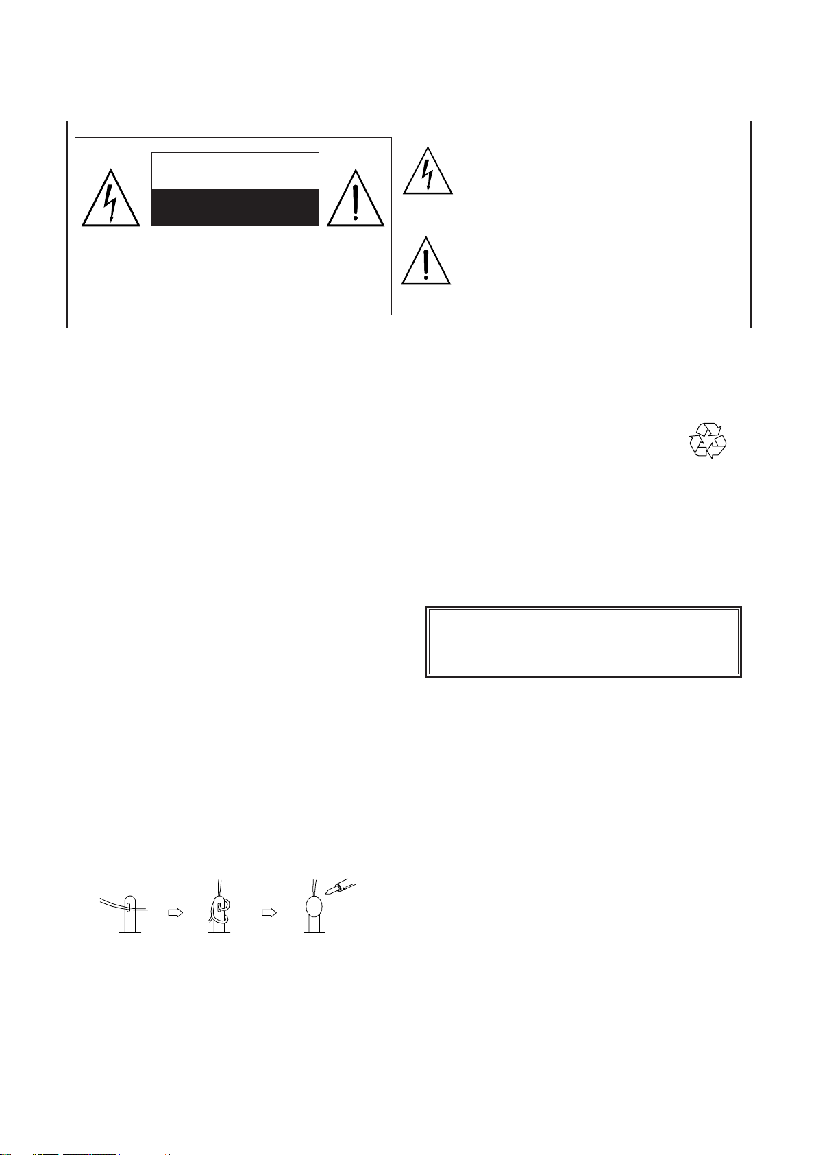
CAUTION
RISK OF ELECTRIC SHOCK
DO NOT OPEN
The lightning flash with arrowhead symbol,
within an equilateral triangle, is intended to
alert the user to the presence of uninsulated
“dangerous voltage” within the product’s enclo
sure that may be of sufficient magnitude to
constitute a risk of electric shock to persons.
CAUTION: TO REDUCE THE RISK OF
ELECTRIC SHOCK, DO NOT REMOVE COVER
(OR BACK). NO USER-SERVICEABLE PARTS
INSIDE. REFER SERVICING TO QUALIFIED
SERVICE PERSONNEL ONLY.
PRECAUTIONS DURING
SERVICING
1. In addition to safety, other parts and
assemblies are specified for conformance with
such regulations as those applying to spurious
radiation. These must also be replaced only
with specified replacements.
Examples: RF converters, tuner units, antenna
selection switches, RF cables, noise-blocking
capacitors, noise-blocking filters, etc.
2. Use specified internal Wiring. Note especially:
1) Wires covered with PVC tubing
2) Double insulated wires
3) High voltage leads
3. Use specified insulating materials for hazardous
live parts. Note especially:
1) Insulating Tape
2) PVC tubing
3) Spacers (insulating barriers)
4) Insulating sheets for transistors
5) Plastic screws for fixing micro switches
4. When replacing AC primary side components
(transformers, power cords, noise blocking
capacitors, etc.), wrap ends of wires securely
about the terminals before soldering.
5. Make sure that wires do not contact heat
generating parts (heat sinks, oxide metal film
resistors, fusible resistors, etc.)
6. Check if replaced wires do not contact sharply
edged or pointed parts.
7. Make sure that foreign objects (screws, solder
droplets, etc.) do not remain inside the set.
The exclamation point within an equilateral
triangle is intended to alert the user to the
presence of important operating and
maintenance (servicing) instructions in the
literature accompanying the appliance.
MAKE YOUR CONTRIBUTION
TO PROTECT THE
ENVIRONMENT
Used batteries with the ISO symbol
for recycling as well as small accumulators
(rechargeable batteries), mini-batteries (cells) and
starter batteries should not be thrown into the
garbage can.
Please leave them at an appropriate depot.
WARNING:
Before servicing this TV receiver, read the
SAFETY INSTRUCTION and PRODUCT
SAFETY NOTICE.
SAFETY INSTRUCTION
The service should not be attempted by anyone
unfamiliar with the necessary instructions on this
apparatus. The following are the necessary
instructions to be observed before servicing.
1. An isolation transformer should be connected in
the power line between the receiver and the
AC line when a service is performed on the
primary of the converter transformer of the set.
2. Comply with all caution and safety related
provided on the back of the cabinet, inside the
cabinet, on the chassis or picture tube.
3. To avoid a shock hazard, always discharge the
picture tube's anode to the chassis ground
before removing the anode cap.
4. Completely discharge the high potential voltage
of the picture tube before handling. The picture
tube is a vacuum and if broken, the glass will
explode.
Page 3
5. When replacing a MAIN PCB in the cabinet,
always be certain that all protective are
installed properly such as control knobs,
adjustment covers or shields, barriers, isolation
resistor networks etc.
6. When servicing is required, observe the original
lead dressing. Extra precaution should be given
to assure correct lead dressing in the high
voltage area.
7. Keep wires away from high voltage or high
tempera ture components.
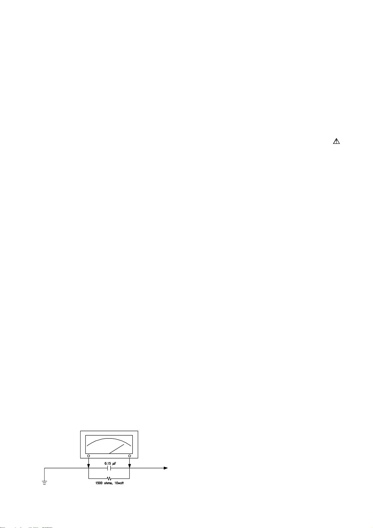
8. Before returning the set to the customer,
always perform an AC leakage current check
on the exposed metallic parts of the cabinet,
such as antennas, terminals, screwheads,metal
overlay, control shafts, etc., to be sure the set
is safe to operate without danger of electrical
shock. Plug the AC line cord directly to the
AC outlet (do not use a line isolation
transformer during this check). Use an AC
voltmeter having 5K ohms volt sensitivity or
more in the following manner.
Connect a 1.5K ohm 10 watt resistor paralleled
by a 0.15µF AC type capacitor, between a
good earth ground (water pipe, conductor etc.,)
and the exposed metallic parts, one at a time.
Measure the AC voltage across the combination
of the 1.5K ohm resistor and 0.15 uF
capacitor. Reverse the AC plug at the AC
outlet and repeat the AC voltage measurements
for each exposed metallic part.
The measured voltage must not exceed 0.3V
RMS.
This corresponds to 0.5mA AC. Any value
exceeding this limit constitutes a potential
shock hazard and must be corrected
immediately.
The resistance measurement should be done
between accessible exposed metal parts and
power cord plug prongs with the power switch
"ON". The resistance should be more than
6M ohms.
AC VOLTMETER
PRODUCT SAFETY NOTICE
Many electrical and mechanical parts in this
apparatus have special safety-related
characteristics.
These characteristics are offer passed
unnoticed by visual spection and the protection
afforded by them cannot necessarily be obtained
by using replacement components rates for a
higher voltage, wattage, etc.
The replacement parts which have these
special safety characteristics are identified by
marks on the schematic diagram and on the parts
list.
Before replacing any of these components,
read the parts list in this manual carefully. The
use of substitute replacement parts which do not
have the same safety characteristics as specified
in the parts list may create shock, fire, or other
hazards.
9. Must be sure that the ground wire of the AC
inlet is connected with the ground of the
apparatus properly.
Good earth ground
such as the water
pipe, conductor,
etc.
AC Leakage Current Check
Place this probe
on each exposed
metallic part
Page 4
Technical Specifications
MODEL :
PDP-5006H
50” Plasma Display
DATE FIRST ISSUED
REVISIONS
ISSUED DATE DESCRIPTION RAISED BY :
ISSUE
1
RAISED BY
CHECKED BY
NUMBER OF PAGES
9
SPECIFICATION AGREED : SIGNATURE DATE
R & D DEPARTMENT
COMMERCIAL DEPARTMENT
PRODUCTION DEPARTMENT
Q/A DEPARTMENT
CUSTOMER
SPECIFICATION APPROVED :
.
NOTE :
Only documents stamped “Controlled Document” to be used for manufacture of production parts.
......................................................................................
......
......................................................................................
......
......................................................................................
.......
......................................................................................
.......
......................................................................................
.......
SIGNATURE :
...........................
...
...........................
...
...........................
...
...........................
...
...........................
...
DATE :
Page 5
Technical Specifications
PDP-5006H
CONTINUATION PAGE
NUMBER
2 OF 9 PAGES
1. Standard Test Conditions
All tests shall be performed under the following conditions, unless otherwise specified.
1.1 Ambient light
≦0.1Cd/m
: 150ux (When measuring IB, the ambient luminance
2
)
1.2 Viewing distance
: 50cm in front of PDP
1.3 Warm up time
: 30 minutes
1.4 PDP Panel facing
: no restricted
1.5 Measuring Equipment
: PC, Chroma 2225 signal generator (with Chroma digital
additional card) or equivalent, Minolta CA100 photometer
1.6 Magnetic field
: no restricted
1.7 Control settings
: Brightness, Contrast, Tint, Color set at Center(50)
1.8 Power input
: 100~240Vac
1.9 Ambient temperature : 20°C ± 5°C (68°F ± 9°F)
1.10 Display mode
: 31.5KHz/60Hz (Resolution 1366 x 768)
1.11 Other conditions
:
1.11.1 With image sticking protection of PDP module, the luminance will descend
by time on a same still screen and rapidly go down in 5 minutes. When
measuring the color tracking and luminance of a same still screen, be sure t
o accomplish the measurement in one minute to ensure its accuracy.
1.11.2 Due to the structure of PDP, the extra-high-bright same screen should not
hold over 5 minutes for fear of branding on the panel.
Page 6
Technical Specifications
PDP-5006H
CONTINUATION PAGE
NUMBER
3 OF 9 PAGES
ELECTRICAL CHARACTERISTICS
2. Power Input
2.1 Voltage
: 100 ~ 240VAC
2.2 Input Current
: 5.0 /2.5A
2.3 Maximum Inrush Current
: <30 A (FOR AC110V ONLY)
Test condition : Measured when switched off for at least 20 mins
2.4 Frequency
: 50Hz to 60Hz(±3Hz)
2.5 Power Consumption
: ≤ 480W
Test condition : full white display with maximum brightness and
contrast
2.6 Power Factor
: Meets IEC1000-3-2
2.7 Withstanding voltage
: 1.5kVac or 2.2kVdc for 1 sec
3. Display
3.1 Screen Size : 50” Plasma display
3.2 Aspect Ratio : 16:9
3.3 Pixel Resolution : 1366x768
3.4 Peak Brightness : 1000 cd/m² (Panel module without filter)
3.5 Contrast Ratio (Dark room) : 5000:1 (Panel module without filter)
3.6 Viewing Angle : Over 160°
3.7 OSD language : English
4. Signal
4.1 AV & Graphic input
4.1.1 Composite signal : CVBS
4.1.2 Y,C Signal : S-Video
4.1.3 Component signal : Y, Pb/Cb, Pr/Cr, HDTV compatible
4.1.4 Graphic I/P : Analog: D-sub 15pin detachable cable
Digital: DVI
4.1.5EDID compatibility : DDC 1.3
4.1.6 I/P frequency : f
: 31.5kHz to 60kHz/fV: 56.25Hz to 75Hz (1024X768
H
recommended)
Page 7
Technical Specifications
PDP-5006H
CONTINUATION PAGE
NUMBER
4 OF 9 PAGES
4.2 Audio input
Audio I/P(L/Rx5) : 1 for DVI / D-Sub
1 for Y/ Pb/Pr
1 for Y/ Cb/Cr
1 for CVBS
1 for S-Video
4.3 AV output
Audio&Video O/P(RCAx3) : Monitor out(Video & Audio L/R)
4.4 Other function
: PIP/POP/PBP, Picture size, Picture Still, Sound mode,Last
memory, Timer, MTS
5. Environment
5.1 Operating environment
5.1.1 Temperature : 5º to 33°C
5.1.2 Relative humidity: 20% to 85%(non-condensing)
5.2 Storage and Transport
5.2.1 Temperature : -20°C to 60°C(-4º to 140°F)
5.2.2 Relative humidity: 5% to 95%
6. Panel Characteristics
6.1 Type : S50HW-XD03
6.2 Size : 50”, 1190mm(width)x7005mm(height)x59mm(depth)±1
mm)
6.3 Aspect ratio : 16:9
6.4 Viewing angle : Over 160°
6.5 Resolution : 1366X768
6.6 Weight : 22.0kg ±0.5 kg (Net)
6.7 Color : 1024(R)X1024(G)X1024(B) COLORS
6.8 Contrast : Average 60:1 (In a bright room with 150Lux at center)
Typical 5000:1 (In a dark room 1/100 White Window
pattern at center).
6.9 Peak brightness : Typical 1000cd/㎡ (1/25 White Window)
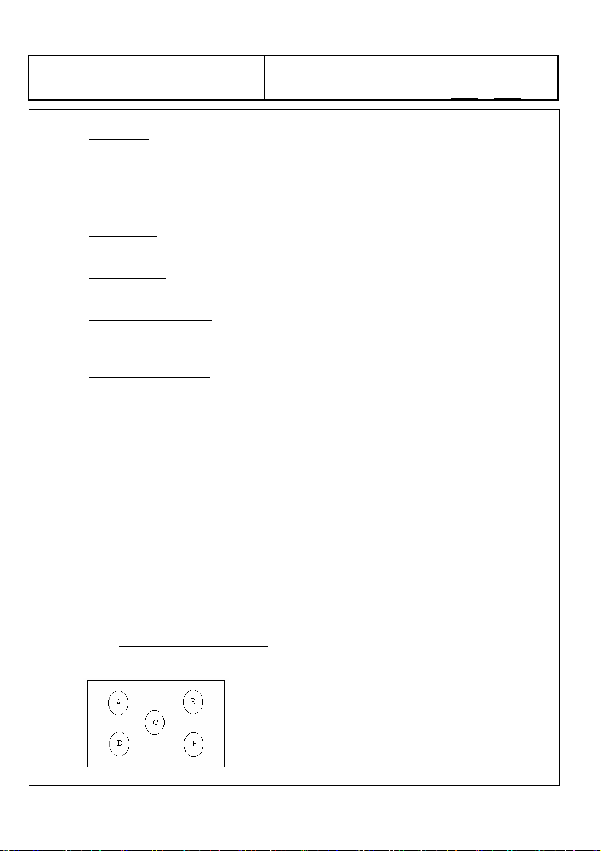
6.10 Color Coordinate Uniformity
: Contrast; Brightness and Color control at normal
setting
Test Pattern : Full white pattern
Average of point A,B,C,D and E +/- 0.01
Page 8

Technical Specifications
PDP-5006H
CONTINUATION PAGE
NUMBER
5 OF 9 PAGES
6.11 Color temperature
: Contrast at center (50); Brightness center (50);
Color temperature set at Natural
x=0.285±0.02
y=0.290±0.02
6.12 Cell Defect Specifications
Subject to Panel supplier specification as appends.
7. Front Panel Control Button
7.1 Sele Up / Down Button : Push the key to select Item up or down.
When selecting the item on OSD menu.
Volume Up/ Down Button : Push the key to increase the volume up or down.
When selecting the adjusting item on OSD menu
increase or decrease the data-bar.
Menu Button : Enter to the OSD menu.
Source Select Button : Push the key to select the input signals source.
7.2 Stand by Button : Switch on main power, or switch off to enter power
Saving modes.
7.3 Main Power Switch : Turn on or off the unit.
8. OSD Function
8.1 Picture : State (Normal,Dark,Bright,User); Display (Bright,contrast,Color,Hue)
Temp (warm,Cool,Normal,User);
Position (H-posit,V-posit,Phase,H-size,Auto Adjust)
8.2 Sound : Setup (Mode,AVC,Volume,Balance);
Equalizer (120HZ,500HZ,1.5KHZ,5KHZ,10KHZ)
BBE Setup (Gain,Treble,Bass)
8.3 OSD : Size (Panorama,16:9,Normal,Anamorphic,Letter Box,TV Mode)
OSD Set (Language,OSD Position,Time Out)
Option (Burn Protect, Version)
V-Chip , C/C
8.4 Layout : Layout (Full Screen,PIP,Split Screen,Grid,POP 3,POP 12)
PIP Set (Sub Win Source,Sub Win Size,PIP Size.PIP Position)
8.5 Time : Sleep (30Min,60Min,90Min,120Min,180Min)
Wake Up (Time Edit,Volume,TV Mode,Channel)
Time Set
Page 9

Technical Specifications
PDP-5006H
CONTINUATION PAGE
NUMBER
6 OF 9 PAGES
9. Agency Approvals
Safety UL60950
Emissions FCC class B
10. Reliability
11.1 MTBF
: 20,000 hours(Use moving picture signal at 25°C ambient)
11. Accessories : User manual x1, Remote control x1, Stand x1, Power cord x1,
Battery x 2, Accessories box x 1,Speaker x 2,Speaker wire x2
Page 10
Technical Specifications
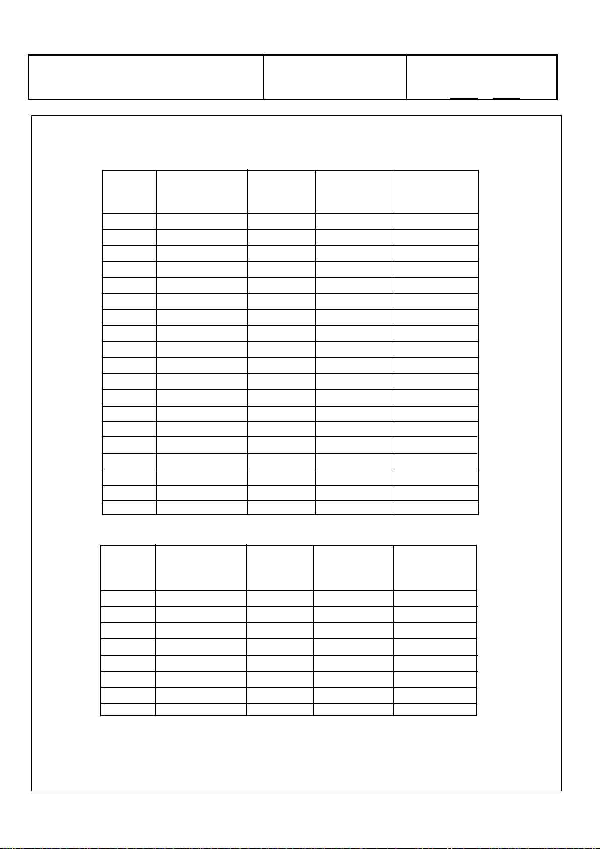
12. Support the Signal Mode
A .D-Sub Mode (VGA or DVI)
PDP-5006H
CONTINUATION PAGE
NUMBER
7 OF 9 PAGES
NO.
1
2
3
4
5
6
7
8
9
10
11
12
13
14
15
16
17
18
19
Resolution
640 x 400
640 x 480
640 x 480
640 x 480
640 x 480
720 x 400
800 x 600
800 x 600
800 x 600
800 x 600
832 x 624
1024 x 768
1024 x 768
1024 x 768
1152 x 864
1152 x 864
1152 x 864
1280 x 960
1280 x 1024
Horizontal
Frequency
(KHz)
31.47
31.50
35.00
37.50
37.86
31.47
35.16
37.90
46.90
48.08
49.00
48.40
56.50
60.00
54.53
63.86
67.52
60.02
64.00
Vertical
Frequency
(Hz)
70.08
60.00
67.00
75.00
72.81
70.08
56.25
60.32
75.00
72.19
74.00
60.00
70.00
75.00
61.13
70.02
75.02
60.02
60.01
Dot Clock
Frequency
(MHz)
25.17
25.18
30.24
31.50
31.50
28.32
36.00
40.00
49.50
50.00
57.27
65.00
75.00
78.75
80.37
94.51
108.03
108.04
108.00
B.DTV Mode
NO.
1
2
3
4
5
6
7
8
Resolution
480 i
576 i
480p(720x480)
576p(720x576)
720p(1280x720)
720p(1280x720)
1080i(1920x1080)
1080i(1920x1080)
Horizontal
Frequency
(KHz)
15.734
15.625
31.468
31.25
45.00
37.50
28.125
33.75
Vertical
Frequency
(Hz)
59.94
50.00
59.94
50.00
60.00
50.00
50.00
60.00
Dot Clock
Frequency
(MHz)
13.50
13.50
27.00
27.00
74.25
74.25
74.25
74.25
- When the signal received by the Display exceeds the allowed range, a warning message “Out Of Range”
shall appear on the screen.
- You can confirm the input signal format from the “OSD Menu”.
Page 11
CONTINUATION PAGE
Technical Specifications
PDP-5006H
NUMBER 8 OF
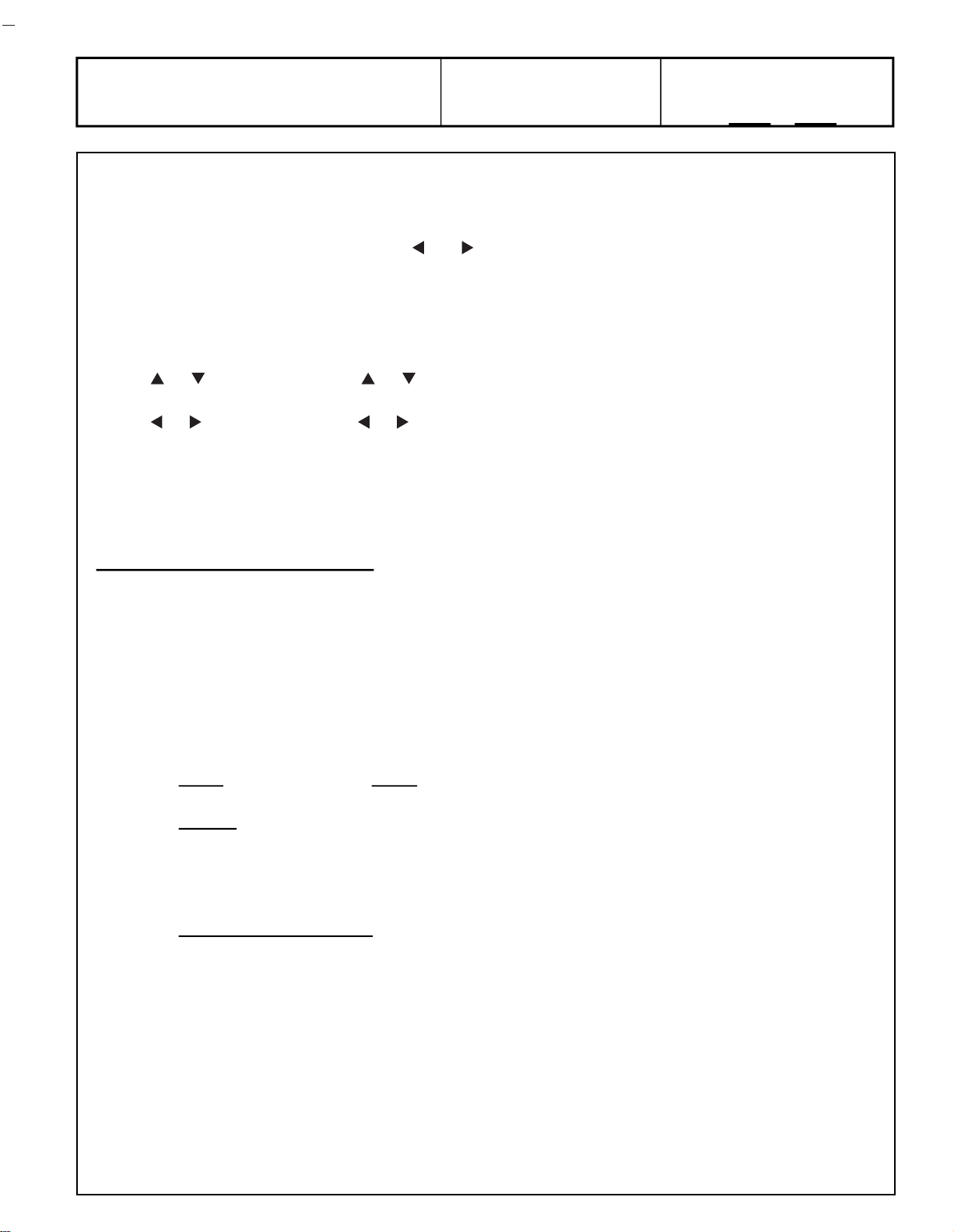
4.4 Remote Control
Power ( ): Press to turn on and off.
Mute (
): Press to mute the sound. Press
again or press ◄ or ► to restore the sound.
P.STILL: Press to freeze the picture. Press
again to restore the picture.
P.SIZE: Press to cycles through the picture
size: Normal, Fill Screen, Anamorphic,
Letter Box, TV Mode or Panorama.
P. MODE: Press to cycles through the picture
mode: NORMAL, BRIGHT, DARK, USER.
S.SELE: Press to cycles through the sound
select: Main window sound or Sub window
sound.
PIP: Press to turns on PIP (picture-in picture) feature. Such as Full Screen, PIP or
Split Screen.
WAP: Press to switches the Main window
S
or Sub window pictures.
C/C: Press to select the Closed Caption
mode.
V-Chip: Press to select the child protect
mode.
TIME: Press to display the current time.
SLEEP: Press repeatedly until it displays
the time in minutes (30 Min, 60 Min, 90 Min,
120 Min, 180 Min or Off ) that you want the
PDP to remain on before shutting off. To
cancel Sleep Time, press SLEEP repeatedly
until Sleep Off appears. And you can press
◄ or ► to select sleep time shut down.
Number buttons: Use these buttons to
enter password.
(Note: The 100 button is inactive in this model.)
PIP Source: Press to select the signal for Sub Window.(Only for PIP.)
F.WHITE: Press to show a full white picture.
INFO: Press to display on-screen information.
SOUND: Press to select different sound system, such as Normal, Flat, News, Cinema,
User or BBE Digital.
PICTURE: Press to select “BRIGHT”, “COLOR”, “CONTRAST”, ”HUE” or “SHARP”, and
you can use◄ or ► to adjust.
EXIT: Press to return or exit OSD menu.
9
PAGES
(Continued on next page)
12
Page 12
CONTINUATION PAGE
Technical Specifications
SOUND: Press to select different sound system, such as Normal, Flat, News, Cinema,
User or BBE Digital.
PICTURE: Press to select “BRIGHTNESS”, “COLOR”, “CONTRAST”, ”HUE” or
“SHARPNESS”, and you can use
EXIT: Press to return or exit OSD menu.
SOURCE: Press to select the signal sources directly. Such as TV, AV1, S-VIDEO,
YCbCr, YPbPr, Analog RGB or Digital RGB.
MENU: Press to display the OSD Menu.
OK: Press to enter or confirm.
used for the selection of the program when the OSD Menu is not shown on the screen.
used for the adjustment of volume when the OSD Menu is not shown on the screen.
/ : They are used as / buttons in the OSD Menu screen and they can be
/ : They are used as
/ buttons in the OSD Menu screen and they can be
or to adjust.
PDP-5006H
NUMBER
9 OF 9 PAGES
PHYSICAL CHARACTERISTICS
14. Power Cord
Length : 1.8m nominal
Type : optional
15. Cabinet
15.1 Color
: silver colour as defined by colour plaque reference number
15.2 Weight
Net weight : 51.8kg
Gross weight : 74kg
15.3 Dimensions (with stand&speak)
Width : 1227.8mm
Height : 739.8mm
Depth : 120.6mm
Page 13
Block Diagram
Product Specification of PDP Module
LVDS Input
Control Signal
(Serial Interface)
APL Data
Memory
Input
Controller
Interface
Controller
Driver
Timing
Controller
Display data, Driver timing
Color Plasma Display Panel
1366 X 768 pixels
Scan Driver
Vs(180V~190V)
Va(55V~65V)
Vcc(+5V)
Common sustain driver
Address Driver
☞ Applied Voltage level is specified at the time when Full-White pattern is displayed on the panel.
Page 14
Block Diagram
Speaker
SCART1
Video2
S-Video
Tuner x 2
Sub Board
TDA8946
Audio AMP
MSP34x0G
Audio Decoder
uPD64083
Separator
M52790
A/V Switch
3D Y/C
Main Board
Z86229
V-Chip / CC
VPC3230D
Vide Decoder
SDA5550
TVText Pro
PW1231
De-
Interlacer
Z86229
V-Chip / CC
VPC3230D
Video Decoder
Processor
PW181
Image
AD9883A
ADC
Sil161B
DVI Receiver
MAX232C
RS232C
W78E65B
System Control
THC63LVDM83
LVDS
Transmitter
YCrCb
YPbPr
D-SUB15
DVI
D-SUB9
IR
Keypad
LED
LDVS
Header
Page 15

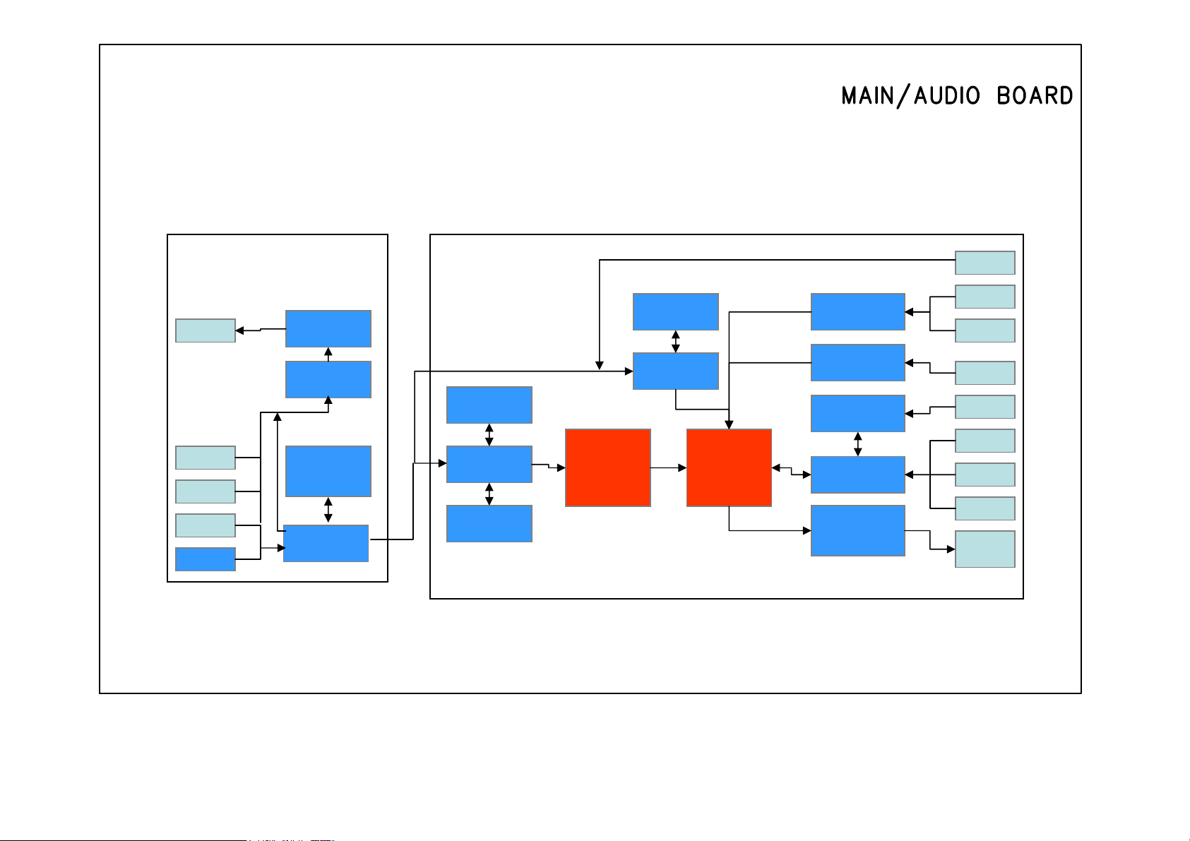
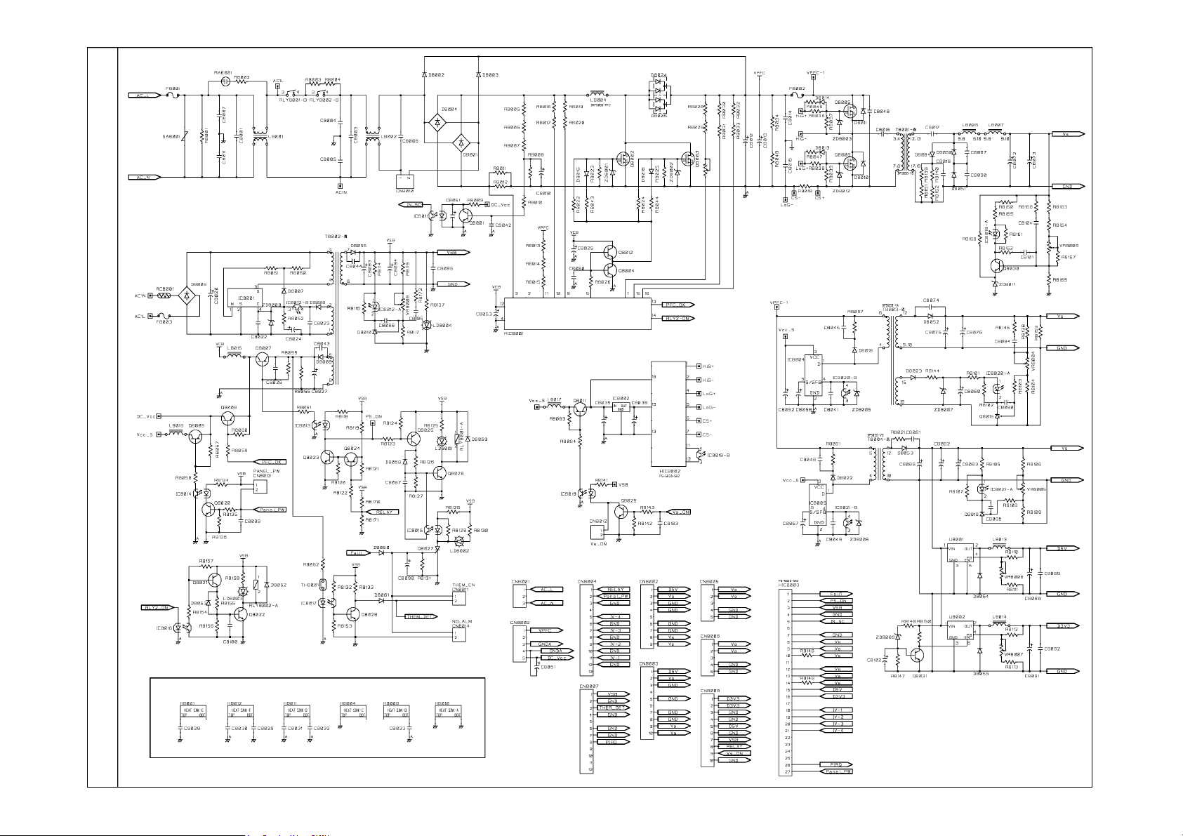
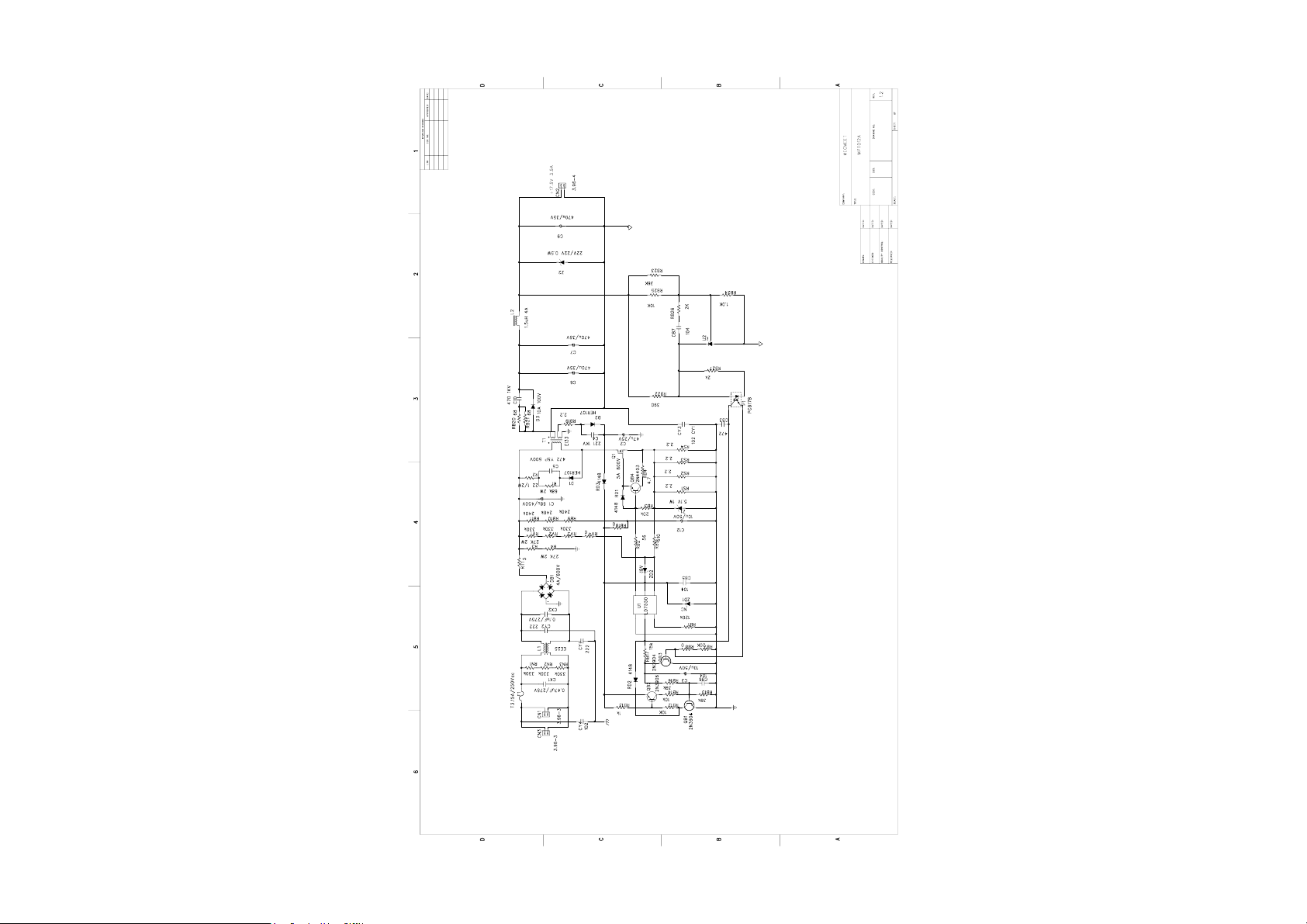
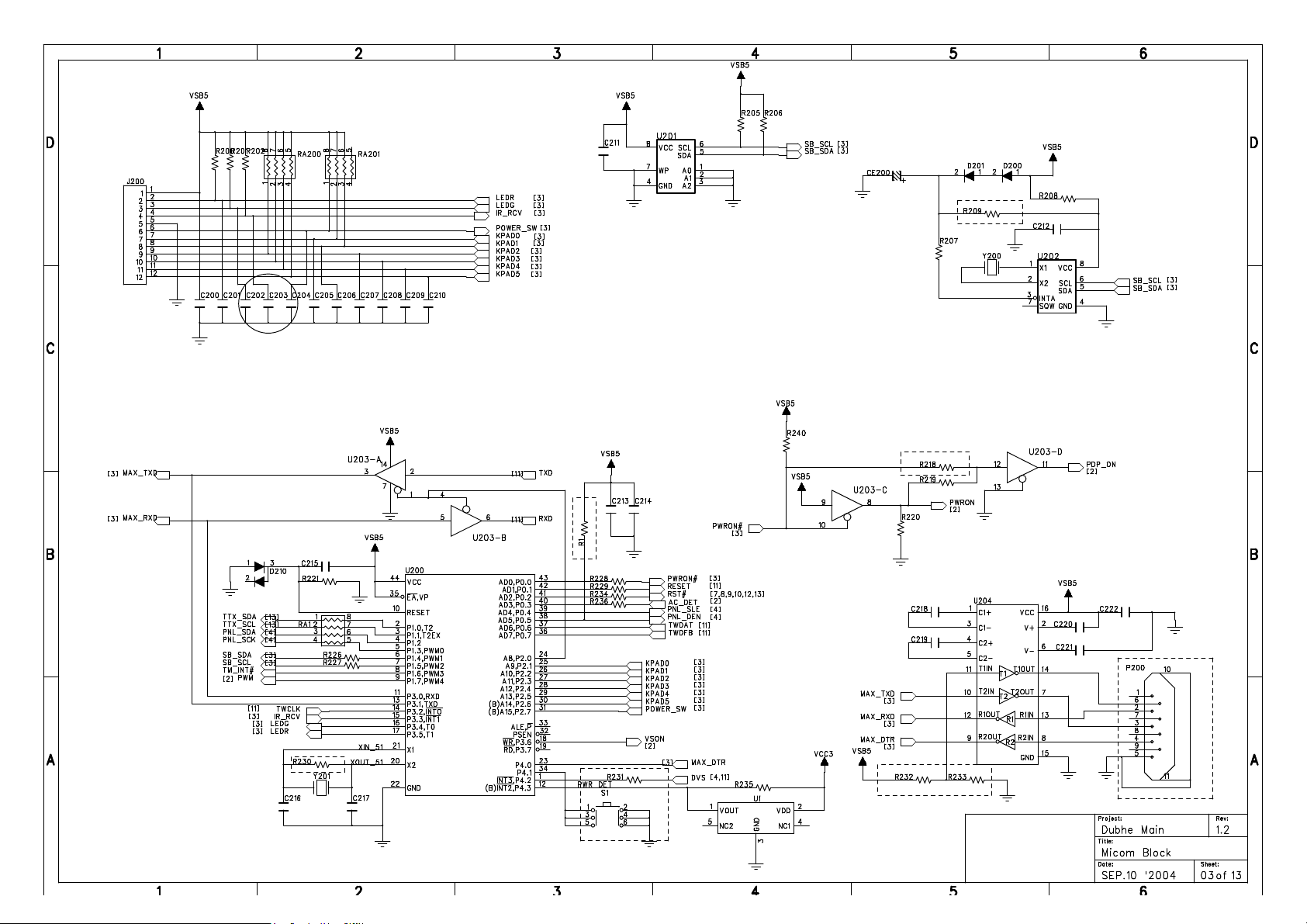
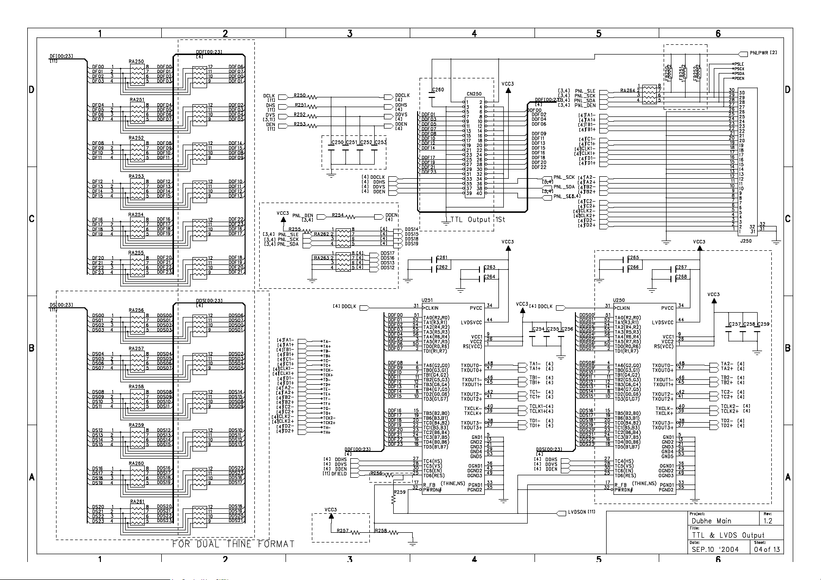
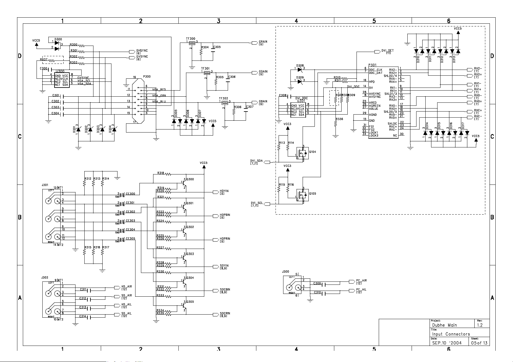
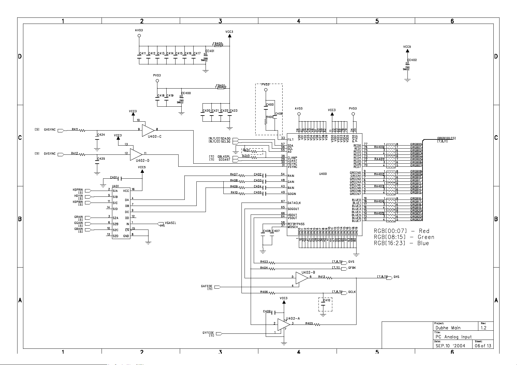
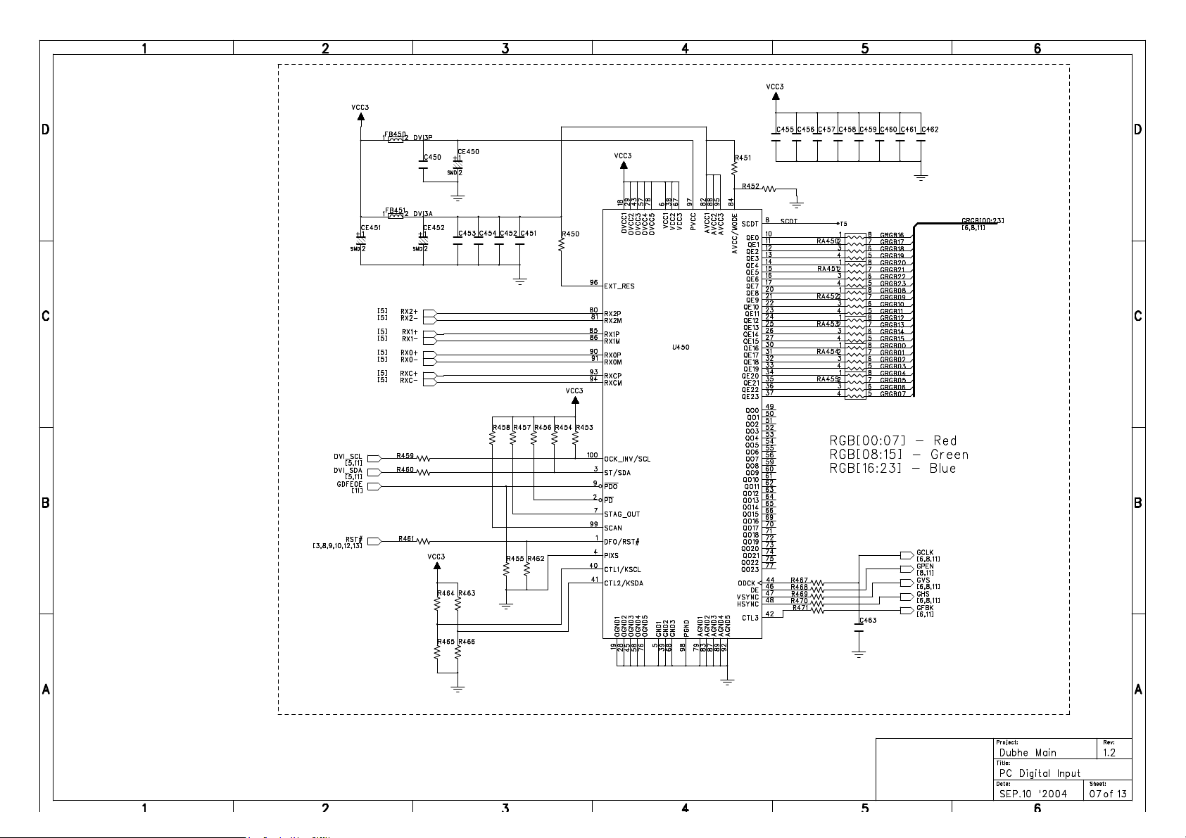
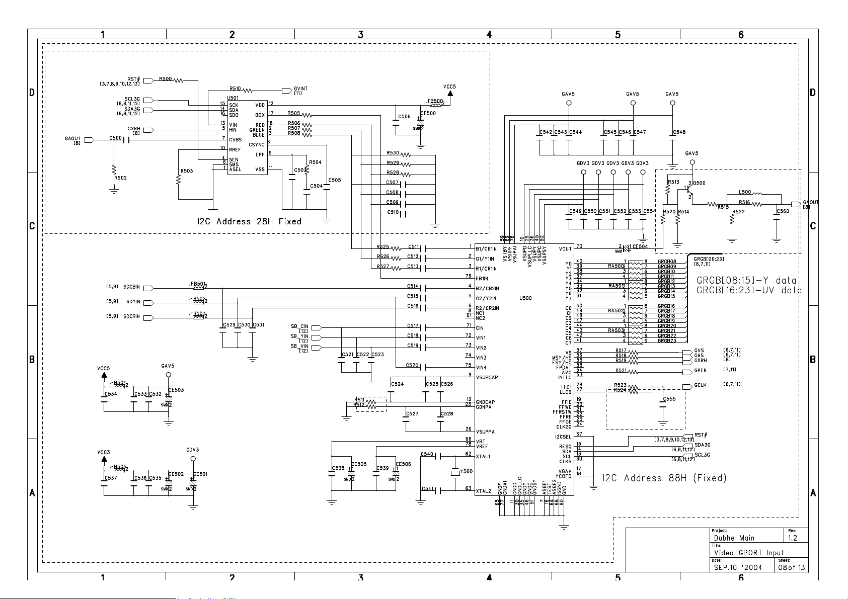
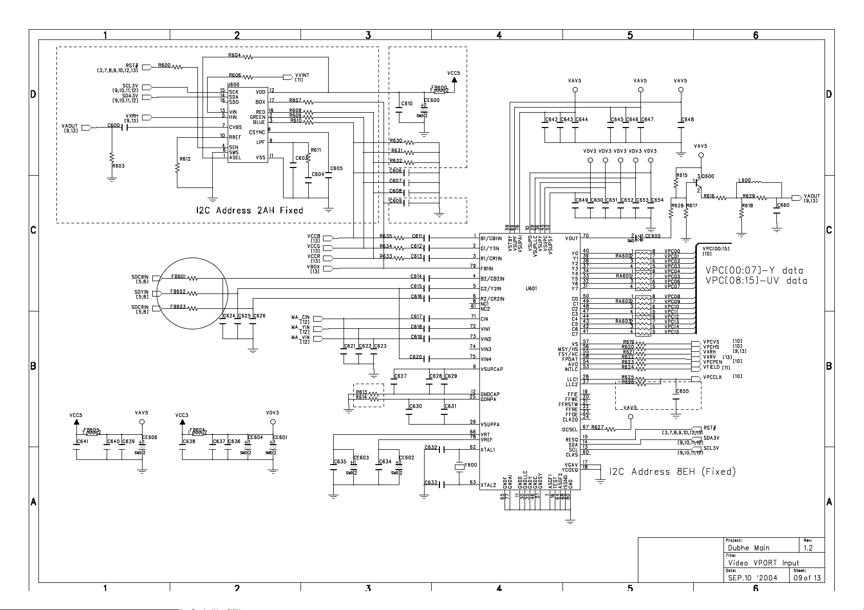
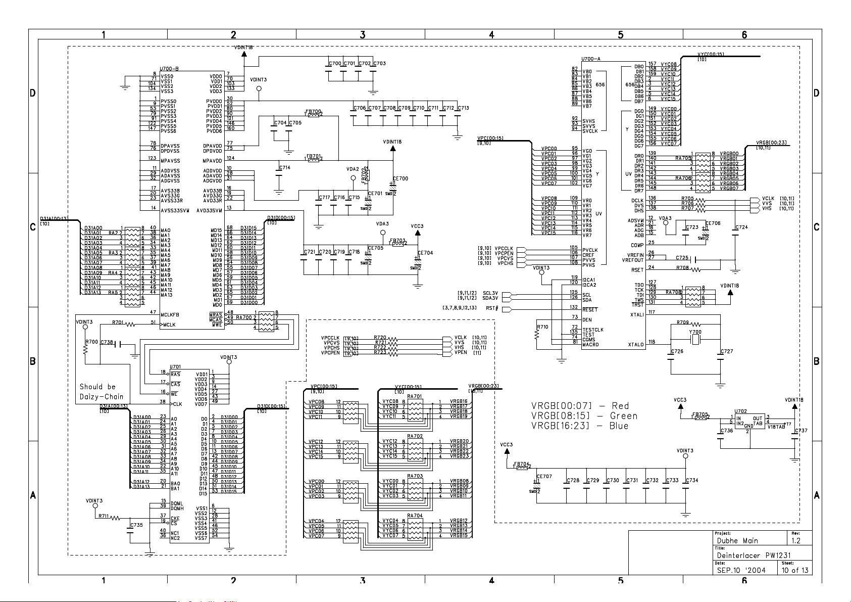
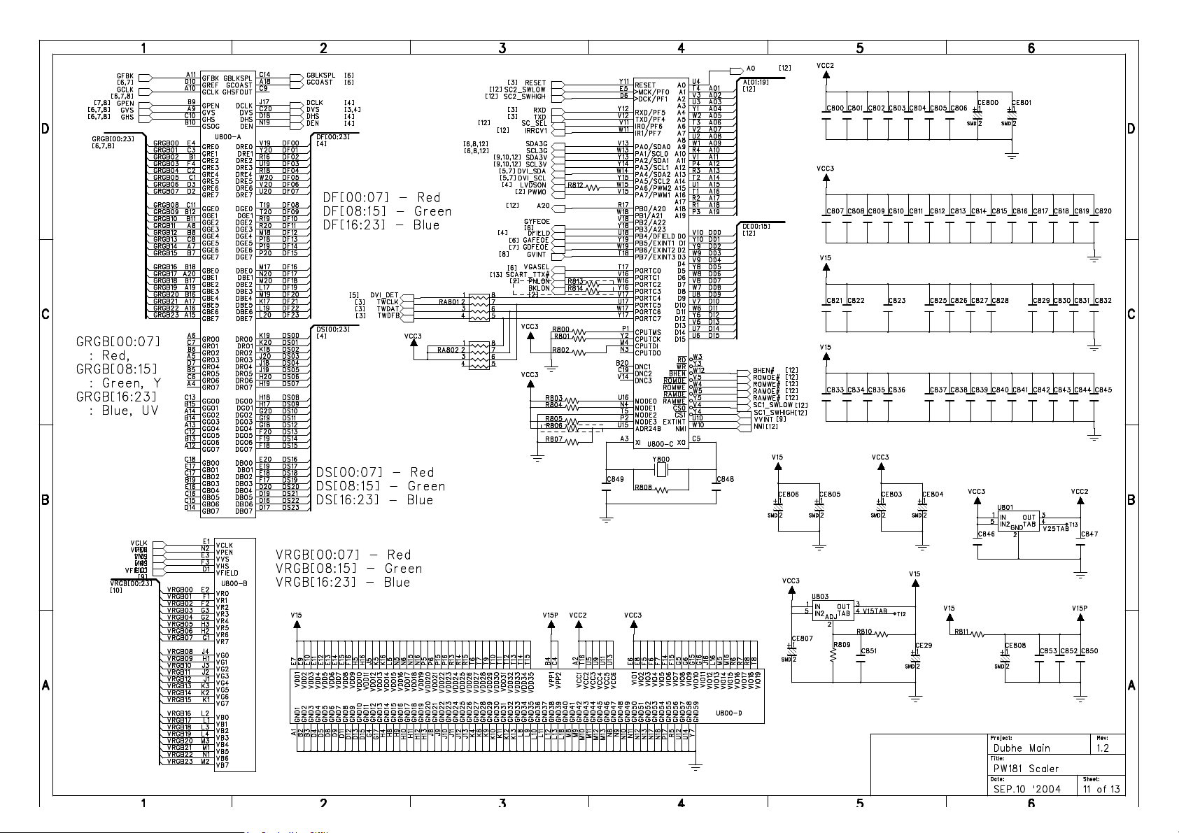
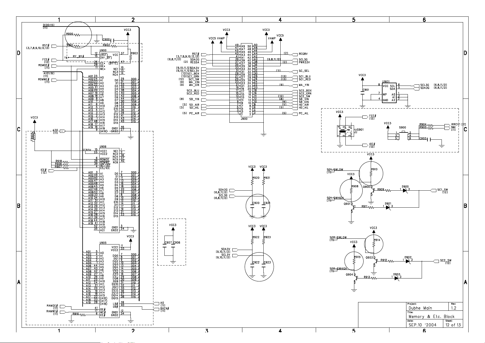
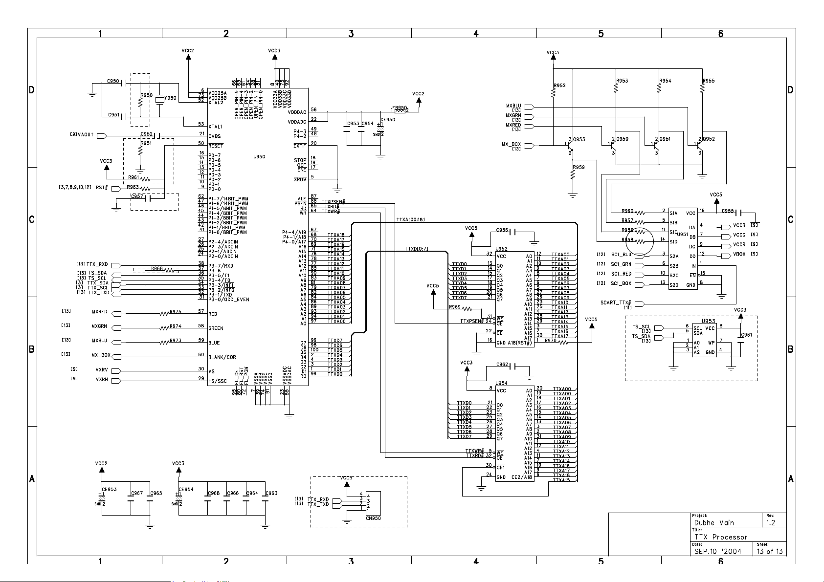
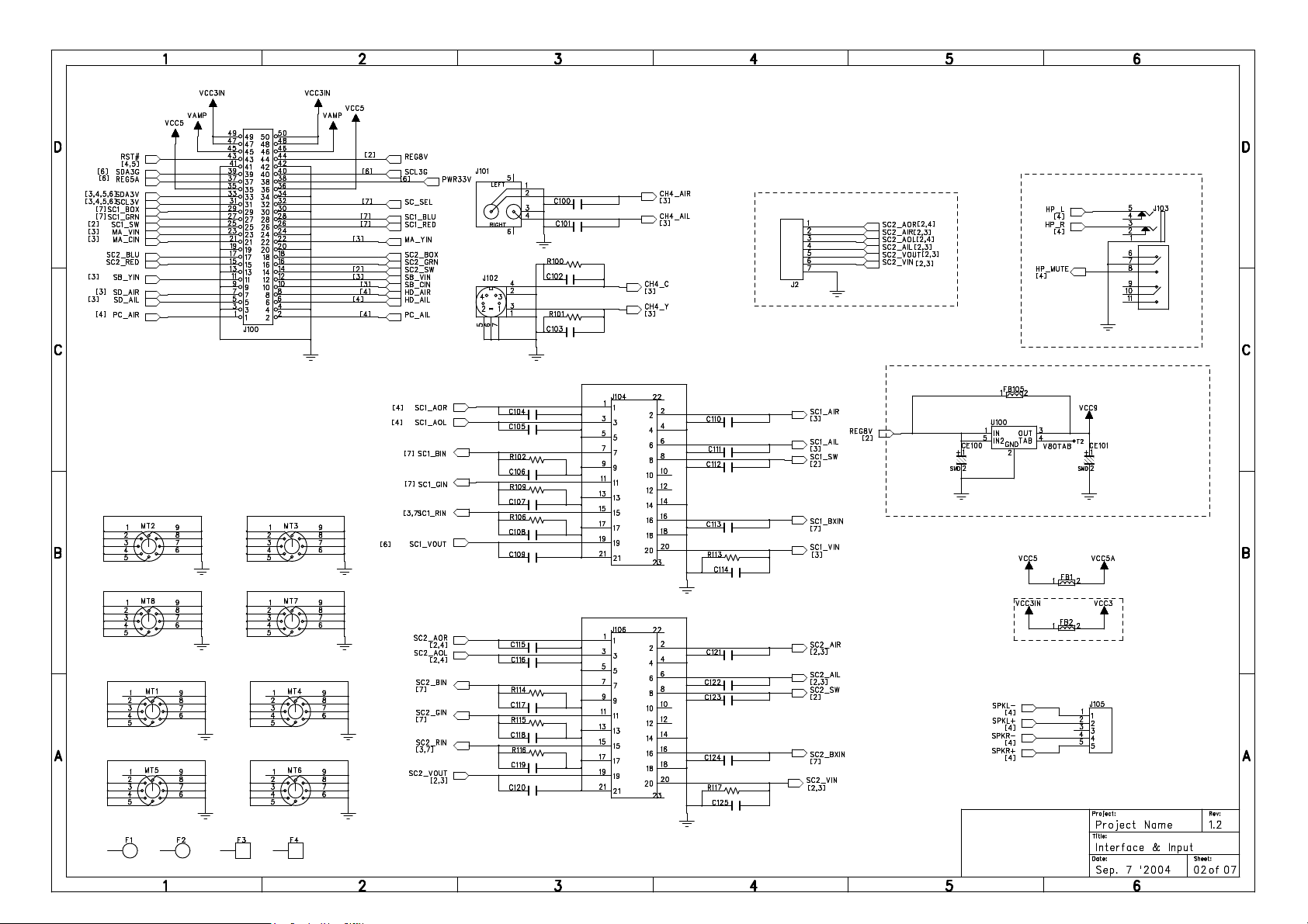
Circuit Diagram
- Power supply board of Audio Amplifier, MPT012A
- Main (Video) board
- Sub (Audio) board
- Keypad board
- Remote control receiver board
- Remote control board
Page 16
Page 17
Page 18
Page 19
Page 20
Page 21
Page 22
Page 23
Page 24
Page 25
Page 26
Page 27
Page 28
Page 29
Dbh1S4909V12.sch-2 - Thu Oct 07 00:30:42 2004
Page 30

Dbh1S4909V12.sch-3 - Thu Oct 07 00:30:43 2004
Page 31

Dbh1S4909V12.sch-4 - Thu Oct 07 00:30:45 2004
Page 32

Dbh1S4909V12.sch-5 - Thu Oct 07 00:30:47 2004
Page 33

Dbh1S4909V12.sch-6 - Thu Oct 07 00:30:49 2004
Page 34

Dbh1S4909V12.sch-7 - Thu Oct 07 00:30:50 2004
Page 35

Dbh2S4909V12.sch-2 - Thu Oct 07 00:32:34 2004
Page 36

DUBHE OSD Ver1.1_NAKS.sch-1 - Mon Oct 18 11:47:11 2004
Page 37

0025.sch-1 - Mon Sep 05 15:03:59 2005
Page 38

Basic Operations & Circuit Description
MODULE
There are 1 pc. panel and 12 pc.s PCB including 2 pc.s Y/Z Sustainer board, 2 pc.s Y Drive
board, 6 pc.s X Extension boards, 1 pc. Control (Signal Input) and 1 pc. Power
board in the Module.
SET
There are 6 pc.s PCBs including 1 pc. AUX. PSU Board, 1 pc. Keypad board, 1 pc.
Remote Control Receiver board, 1 pc. L/R Speakers and 1 pc. Main (Video) board in the SET.
Page 39

Y-Driver Top
Y-Sustainer
Y-Driver Bottom
X-extension Bottom L/C/R
Local Key
Stand
Main (Video)
Sub(Audio)
EMI Filter & AC
Inlet
X-extension Top L/C/R
Power Supply
Control board Assy.
External Speaker
Terminals
Z-Sustainer
AUX PSU Board
Page 40

PCB function
1. Power:
(1). Input voltage: AC 110V~240V, 47Hz~63Hz.
Input range: AC 90V(Min)~265V(Max) auto regulation.
(2). To provide power for PCBs.
2. Main (Video InterFace) board: To process S-video signals, AV signals, Y Pb/
Cb Pr/Cr signals, DVI signals and D-SUB signals to digital ones and to transmit to
Control board.
3. Control board: Dealing with the digital signal(LVDS) for output to panel.
4. Y-Sustainer / Z-Sustainer board:
(1). Receiving the signals from Control and high voltage supply.
(2). Output scanning waveform for Module.
5. Y-Drive board: Receive signal from Y sustainer, output horizontal scanning waveform to the panel.
6. X extension board (6pcs): Output addressing signals.
7. Audio Board
: :
: Process and Amplifying the audio signal to speakers .
: :
Page 41

PCB failure analysis
1. CONTROL : a. Abnormal noise on screen. b. No picture.
2. MAIN (video) : a. Lacking color, Bad color scale.
b. No voice.
c. No picture but with signals output, OSD and back light.
d. Abnormal noise on screen.
3. POWER : No picture, no power output.
4. Z - Sustainer :a. No picture.
b. Color not enough.
c. Flash on screen.
5. Y - Sustainer : Darker picture with signals.
6. X - Extension : Abormal vertical noise on screen.
7. Audio Board or AUX PSU: a. No voice. (Make sure Mute/OFF) .
b. Noise.
Page 42

Basic operation of Plasma Display
1. After turning on power switch, power board sends 5Vst-by Volt to Micro Processor
2. The micro Processor memorize the last state of Power, When the last state of
power is on or receive power on signal from local Key or Remote control, Micro
Processor will send on control signal to power. Then Power sends (5Vsc, 9Vsc,
24V and RLYON, Vs ON) to PCBs working. This time Main will send signals to
display Image, OSD on the panel and start to search available signal sources.
If the audio signals input, them will be amplified by Audio AMP and transmitted to
Speakers.
3. If some abnormal signals are detected (for example: over volts, over current, over
temperature and under volts), the system will be shut down by Power off.
Page 43

Main IC Specifications
- PW181 Image Processor, Scaler
- PW1231 Digital Video Signal Processor
- uPD64083 Three –Dimensional Y/C Separation LSI
With On-Chip Memory
- AD9883A 110MSPS/140MSPS Analog Interface
- VPC 323XD Comb-filter Video Processor
- Si161B Panel Link Receiver
- Z86229 NTSC Line 21 CCD decorder
- MSP34x0G Multistandard Sound Processor
Page 44

PW181
Product Specification
General Description
The PW181 ImageProcessor is a highly integrated
“system-on-a-chip” that interfaces computer graphics and
video inputs in virtually any format to a fixed-frequency flat
panel display.
Computer and video images from NTSC/PAL to WUXGA
at virtually any refresh rate can be resized to fit on a fixedfrequency target display device with any resolution up to
WUXGA. Video data from 4:3 aspect ratio NTSC or PAL
and 16:9 aspect ratio HDTV or SDTV is supported. Multiregion, nonlinear scaling allows these inputs to be resized
optimally for the native resolution of the display.
Advanced scaling techniques are supported, such as
format conversion using multiple programmable regions.
Three independent image scalers coupled with frame
locking circuitry and dual programmable color lookup
tables create sharp images in multiple windows, without
user intervention.
Embedded SDRAM frame buffers and memory controllers
perform frame rate conversion and enhanced video
processing completely on-chip. A separate memory is
dedicated to storage of on-screen display images and
CPU general purpose use.
Advanced video processing techniques are supported
using the internal frame buffer, including motion adaptive,
temporal deinterlacing with film mode detection. When
used in combination with the new third-generation scaler,
this advanced video processing technology delivers the
highest quality video for advanced displays.
Both input ports support integrated DVI 1.0 content
protection using standard DVI receivers.
A new advanced OSD Generator with more colors and
larger sizes supports more demanding OSD applications,
such as on-screen programming guides. When coupled
with the new, faster, integrated microprocessor, this OSD
Generator supports advanced OSD animation techniques.
Video
TV
Signal
Input
TV Tu n e r
Com puter
Video
Decoder
ADC/
TMDS
Crystal
PW181
TV
Signal
Com puter
TV Tu n e r
Video
Input
ADC/
TMDS
Video
Decoder
PW181 System Block Diagram
ROM
Features
• Third-generation, two-dimensional filtering techniques
• Third-generation, advanced scaling techniques
• Second-generation Automatic Image Optimization
• Frame rate conversion
• Video processing
• On-Screen Display (OSD)
• On-chip microprocessor
• JTAG debugger and boundary scan
• Picture-in-picture (PIP)
• Multi-region, non-linear scaling
• Hardware 2-wire serial bus support
Applications
• Multimedia Displays
• Plasma Displays
• Digital Television
Device Application Package
PW181-10V Up to XGA Displays
PW181-20V Up to UXGA Displays
352 PBGA
Dis pla y
Programmable features include the user interface, custom
start-up screen, all automatic imaging features, and
special screen effects.
PRELIMINARY / CONFIDENTIAL
Page 45

110 MSPS/140 MSPS Analog Interface
a
FEATURES
140 MSPS Maximum Conversion Rate
300 MHz Analog Bandwidth
0.5 V to 1.0 V Analog Input Range
500 ps p-p PLL Clock Jitter at 110 MSPS
3.3 V Power Supply
Full Sync Processing
Sync Detect for “Hot Plugging”
Midscale Clamping
Power-Down Mode
Low Power: 500 mW Typical
4:2:2 Output Format Mode
APPLICATIONS
RGB Graphics Processing
LCD Monitors and Projectors
Plasma Display Panels
Scan Converters
Microdisplays
Digital TV
R
AIN
G
AIN
B
AIN
HSYNC
COAST
CLAMP
FILT
SCL
SDA
for Flat Panel Displays
FUNCTIONAL BLOCK DIAGRAM
CLAMP
CLAMP
CLAMP
SYNC
PROCESSING
AND CLOCK
GENERATION
SERIAL REGISTER
AND
A
0
POWER MANAGEMENT
A/D
A/D
A/D
AD9883A
8
R
OUTA
8
G
OUTA
8
B
OUTA
MIDSCV
DTACK
HSOUT
VSOUT
SOGOUT
REF
AD9883A
REF
BYPASS
GENERAL DESCRIPTION
The AD9883A is a complete 8-bit, 140 MSPS monolithic analog
interface optimized for capturing RGB graphics signals from
personal computers and workstations. Its 140 MSPS encode
rate capability and full power analog bandwidth of 300 MHz
supports resolutions up to SXGA (1280 × 1024 at 75 Hz).
The AD9883A includes a 140 MHz triple ADC with internal
1.25 V reference, a PLL, and programmable gain, offset, and
clamp control. The user provides only a 3.3 V power supply,
analog input, and Hsync and COAST signals. Three-state
CMOS outputs may be powered from 2.5 V to 3.3 V.
The AD9883A’s on-chip PLL generates a pixel clock from the
Hsync input. Pixel clock output frequencies range from 12 MHz to
140 MHz. PLL clock jitter is 500 ps p-p typical at 140 MSPS.
When the COAST signal is presented, the PLL maintains its
output frequency in the absence of Hsync. A sampling phase
adjustment is provided. Data, Hsync, and clock output phase
relationships are maintained. The AD9883A also offers full sync
processing for composite sync and sync-on-green applications.
A clamp signal is generated internally or may be provided by
the user through the CLAMP input pin. This interface is fully
programmable via a 2-wire serial interface.
Fabricated in an advanced CMOS process, the AD9883A is
provided in a space-saving 80-lead LQFP surface-mount plastic
package and is specified over the 0°C to 70°C temperature range.
REV. A
Information furnished by Analog Devices is believed to be accurate and
reliable. However, no responsibility is assumed by Analog Devices for its
use, nor for any infringements of patents or other rights of third parties that
may result from its use. No license is granted by implication or otherwise
under any patent or patent rights of Analog Devices.
One Technology Way, P.O. Box 9106, Norwood, MA 02062-9106, U.S.A.
Tel:
Fax:
Page 46

PW1231A
Product Specification
General
The PW1231A is a high-quality, digital video signal
processor that incorporates Pixelworks’ patented
deinterlacing, scaling, and video enhancement
algorithms. The PW1231A accepts industry-standard
video formats and resolutions, and converts the input into
many desired output formats.The highly efficient video
algorithms result in excellent quality video.
The PW1231A combines many functions into a single
device, including a memory controller, auto-configuration,
and others. This high level of integration enables simple,
flexible, cost-effective solutions that require fewer
components.
Crysta l
Video
PW1231A
System Block Dia gram
Video
Decoder
PW1231A
PW1231AL
SDRAM
Digital
Output
Features
• Built-In Memory Controller
• Motion-Adaptive Deinterlace Processor
• Intelligent Edge Deinterlacing
• Digital Color/Luminance Transient Improvement (DCTI/DLTI)
• Interlaced Video Input Options, including NTSC and PAL
• Independent horizontal and vertical scaling
• Copy Protection
• Two-Wire Serial Interface
8100 SW Nyberg Road
Tualatin, OR 97062 USA
Telephone: 503.612.6700
FAX: 503.612.6713
www.pixelworks.com
Applications:
For use with Digital Displays
• Flat-Panel (LCD, DLP) TVs
• Rear Projection TVs
• Plasma Displays
• LCD Multimedia Monitors
• Multimedia Projectors
Device Application Package
PW1231A
PW1231AL
NOTE: “L” denotes lead (Pb) free
Up to XGA 160-pin PQF
P/N 001-0097-00 Rev B
PRELIMINARY—CONFIDENTIAL
July 2003
Page 47

DATA SHEET
MOS INTEGRATED CIRCUIT
PD64083
µµµµ
THREE-DIMENSIONAL Y/C SEPARATION LSI WITH ON-CHIP MEMORY
DESCRIPTION
The µPD64083 realizes a high precision Y/C separation and a noise reduction by the three-dimension signal
processing for NTSC signal.
This product has the On-chip 4-Mbit memory for flame delay, 2ch of high precision internal 10-bit A/D converter, and
adapting 10-bit signal processing (only for luminance signal) and high picture quality. The
single-chip system of 3D Y/C separation.
This LSI includes the Wide Clear Vision ID signal (Japanese local format) decoder and ID-1 signal decoder.
PD64083 is completely
µ
FEATURES
•
On-chip 4-Mbit frame delay memory.
•
4 Operation mode (Compatible to the µPD64082)
Motion adaptive 3D Y/C separation (for Composite video input)
Frame recursive Y/C NR (for Y/C separated video input)
Frame comb type YNR + 1H delayed C signal (for Y/C separated video input)
2D Y/C separation + Frame recursive Y/C NR (for Composite video input)
•
Embedded A/D converter (2ch), D/A converter (2ch), clock generator.
•
Embedded Y coring, Vertical enhancer, Peaking filter, and Noise detector.
•
Embedded WCV-ID decoder and ID-1 decoder.
•
I2C bus control.
•
Dual power supply of 2.5 V and 3.3 V.
For digital : DV
For analog : AV
For DRAM : DV
For I/O : DV
DDIO
= 2.5 V
DD
= 2.5 V
DD
DDRAM
= 3.3 V
= 2.5 V
ORDERING INFORMATION
Part number Package
PD64083GF-3BA 100-pin plastic QFP (14 × 20)
µ
Document No. S15849EJ1V0DS00 (1st edition)
Date Published January 2002 NS CP (K)
Printed in Japan
2
Page 48

PRELIMINARY DATA SHEET VPC 323xD
Comb Filter Video Processor
1. Introduction
The VPC 323xD is a high-quality, single-chip video
front-end, which is targeted for 4: 3 and 16:9, 50/60-Hz
and 100/120 Hz TV sets. It can be combined with other
members of the DIGIT3000 IC family (such as
DDP 331x) and/or it can be used with 3rd-party products.
The main features of the VPC 323xD are
– high-performance adaptive 4H comb filter Y/C sepa-
rator with adjustable vertical peaking
– multi-standard color decoder PAL/NTSC/SECAM
including all substandards
– four CVBS, one S-VHS input, one CVBS output
– two RGB/YC
component inputs, one Fast Blank
rCb
(FB) input
– integrated high-quali ty A/D converters and associ-
ated clamp and AGC circuits
– multi-standard sync proces sing
– linear horizontal scaling (0.25 ... 4), as well as
non-linear horizontal scaling ‘Panoramavision’
– PAL+ preprocessing
– peak ing, contrast, brightness, color saturation and
tint for RGB/YC
and CVBS/S-VHS
rCb
– high-qual ity soft mixer controlled by Fast Blank
1
1
1
----- -
-- -
– PIP processing for four picture sizes ( , or
1
---
of normal size) with 8-bit resolution
36
---
,,
4
16
9
– 15 predefined PIP display configurations and expert
mode (fully programmable)
– control interface for external field memory
2
–I
C-bus interface
– one 20.25-MHz crystal, few external components
– 80-p in PQFP pack age
1.1. System Architecture
Fig.1–1 shows the block diagram of the video processor
– li ne-locked c lock, data and sync, or 656-output
interface
CIN
VIN1
VIN2
VIN3
VIN4
VOUT
RGB/
YCrCb
FB
RGB/
YCrCb
Analog
Front-end
AGC
2×ADC
Analog
Component
Front-End
4 x ADC
Adaptive
Comb
Filter
NTSC
PAL
Y/G
Processing
U/B
V/R
FB FB
Matrix
Contrast
Saturation
Brightness
Tint
Color
Decoder
NTSC
PAL
SECAM
Saturation
Tint
Y
Cr
Cb
Y
Cr
Cb
Mixer
Y
2D Scaler
Panorama
Cr
Cb
Brightness
Clock
Gen.
PIP
Mode
Contrast
Peaking
2
I
C Bus
Output
Formatter
ITU-R 656
ITU-R 601
Memory
Control
Sync
+
Clock
Generation
Y OUT
CrCb
OUT
YCOE
FIFO
CNTL
LL C lock
H Sync
V Sync
AVO
Fig.1–1:Block diagram of the VPC323xD
Micronas
2
C Bus20.25 MHz
I
Page 49

SiI 161B PanelLink® Receiver
Data Sheet
General Description Features
The SiI 161B receiver uses PanelLink Digital
technology to support high-resolution displays up to
UXGA (25-165MHz). This receiver supports up to true
color panels (24 bits per pixel, 16M colors) with both
one and two pixels per clock.
All PanelLink products are designed on a scaleable
CMOS architecture, ensuring support for future
performance enhancements while maintaining the
same logical interface. System designers can be
assured that the interface will be stable through a
number of technology and performance generations.
PanelLink Digital technology simplifies PC and display
interface design by resolving many of the system level
issues associated with high-speed mixed signal design,
providing the system designer with a digital interface
solution that is quicker to market and lower in cost.
• Low Power Operation: 280mA max. current
consumption at 3.3V core operation
• Time staggered data output for reduced ground
bounce and lower EMI
• Sync Detect feature for Plug & Display
• Cable Distance Support: over 5m with twisted-
pair, fiber-optics ready
• ESD tolerant to 5kV (HBM on all pins)
• Compliant with DVI 1.0 (DVI is backwards
compatible with VESA
®
P&DTM, FPDI-2
DFP)
• HSYNC de-jitter circuitry enables stable operation
even when HSYNC contains jitter
• Low power standby mode
• Automatic entry into standby mode with clock
detect circuitry
• Standard and Pb-free packages (see page 25).
August 2002
TM
and
Page 50

4'.+/+0#4; 41&7%6#2'%+(+%#6+10
<
+0'
'%1&'4
• Complete Stand-Alone Line 21 Decoder for Closed-
Captioned and Extended Data Services (XDS)
• Preprogrammed to Provide Full Compliance with
EIA–608 Specifications for Extended Data Services
• Automatic Extraction and Serial Output of Special
XDS Packets (Time of Day, Local Time Zone, and
Program Blocking)
• Programmable XDS Filter for a Specific XDS Packet
• Cost-Effective Solution for NTSC Violence Blocking
inside Picture-in-Picture (PiP) Windows
!"
#$%
&%
" '
• Minimal Communications and Control Overhead Pro-
vide Simple Implementation of Violence Blocking,
Closed Captioning, and Auto Clock Set Features
• Programmable, On-Screen Display (OSD) for Creat-
ing Full Screen OSD or Captions inside a Picture-inPicture (PiP) Window
• User-Programmable Horizontal Display Position for
easy OSD Centering and Adjustment
2
• I
C Serial Data and Control Communication
• Supports 2 Selectable I
2
C Addresses
Capable of processing Vertical Blanking Interval (VBI)
data from both fields of the video frame in data, the Z86229
Line 21 Decoder offers a feature-rich solution for any television or set-top application. The robust nature of the
Z86229 helps thedevice conformto thetransmission format
defined in the Television Decoder Circuits Actof 1990,and
in accordance with the Electronics Industry Association
specification 608 (EIA–608).
The Line 21data stream can consist of data from several data
channels multiplexed together. Field 1 consists of four data
channels: two Captions and two Texts. Field 2 consists of
five additional data channels: two Captions, two Texts, and
Extended Data Services (XDS). The XDS data structure is
defined in EIA–608. The Z86229 can recover and display
data transmitted on any of these nine data channels.
The Z86229 can recover and output to a host processor via
2
C serial bus. The recovered XDS data packet isfurther
the I
defined in the EIA–608 specification. The on-chip XDS filters in the Z86229 are fully programmable, enabling recovery ofonly those XDS data packetsselected bythe user.This
functionality allows the device to extract the required XDS
information with proper XDS filter setup for compatibility
in a variety of TVs, VCRs, and Set-Top boxes.
In addition, the Z86229 is ideally suited to monitor Line 21
video displayed in a PiP window for violence blocking,
CCD, and other XDS data services. A block diagram of the
Z86229 is illustrated in Figure 1.
Page 51

PRELIMINARY DATA SHEET MSP 34x0G
Multistandard Sound Processor Family
Release Note: Revision bars indicate significant
changes to the previous edition. The hardware and
software description in this document is valid for
the MSP 34x0G version B8 and following versions.
1. Introduction
The MSP 34x0G family of single-chip Multistandard
Sound Processors covers the sound processing of all
analog TV-Standards worldwide, as well as the NICAM
digital sound standar ds. The full TV sound process ing ,
starting with analog sound IF signal-in, down to processed analog AF-out, is performed on a single chip.
Figure 1–1 shows a simplified functional block diagram
of the MSP 34x0G.
This new generation of TV sound processing ICs now
includes versions for processing the multichan nel television sound (MTS) signal conforming to the standard
recommended by the Broadcast Television Systems
Committee (BTSC). The DBX noise reduction, or alternatively, Micronas Noise Reduction (MNR) is performed alignment free.
Other processed standards are the Japanese FM-FM
multiplex standard (EIA-J) and the FM Stereo Radio
standard.
Current ICs have to perform adjustment procedu res in
order to achieve good stereo sepa ration for BTSC and
EIA-J. The MSP 34x0G has optimum stereo performance without any adjustments.
All MSP 34xxG versions are pin compatible to the
MSP 34xxD. Only minor modifications are necessary
to adapt a MSP 34xxD controlling software to the
MSP 34xxG. The MSP 34x0G further simplifies controlling software. St andard selection requi res a single
2
C transmission only.
I
The MSP 34x0G has built-in automatic functions: The
IC is able to detect the actual sound standard automatically (Automatic Standard Detection). Furthermore,
pilot levels and identification sign als can be evaluated
internally with subsequent switching between mono/
stereo/bilingual; no I
2
C interaction is necessar y (Auto-
matic Sound Selectio n) .
The MSP 34x0G can handle very high FM deviations
even in conjunction with NICAM processing. This is
especially impor tant for the introduction of NICAM in
China.
The ICs are produced in submicron CMOS technology.
The MSP 34x0G is available in the following packages:
PLCC68 (not intended for new design), PSDIP64,
PSDIP52, PQFP80, and PLQFP64.
Sound IF1
Sound IF2
I2S1
I2S2
SCART1
SCART2
SCART3
SCART4
MONO
ADC
SCART
DSP
Input
Select
De-
modulator
ADC
Pre-
processing
Prescale
Prescale
Fig. 1–1: Simplified functional block diagram of the MSP 34x0G
Loud-
speaker
Sound
Processing
Headphone
Sound
Processing
Source Select
DAC
DAC
DAC
DAC
SCART
Output
Select
Loudspeaker
Subwoofer
Headphone
I2S
SCART1
SCART2
Micronas
Page 52

MODEL : 50" HD D3.1 PDP
1,269cm (50 Inch) Wide Plasma Display Module
Quality Innovation Team
1 / 37
Page 53

Samsung SDI Co. Ltd. A/S Manual Plasma Display Module
PDP Division, Samsung SDI
1.Overview
1-1 Model Name of plasma Display
1-2 External View
1-3 Specifications
2. Precaution
2-1 Handling Precaution for Plasna Display,
CONTENTS
2-2
Safety Precautions for Service (Handling, prevention of a electrical shock, measure against
power outage, etc)
3. Name & Function
3-1 Layout of Assemblies
3-2 Block Diagram:
3-3 Main function of Each Assembly
3-4 Product/Serial Label Location
4. Operation checking after rectification
4-1 Flow chart
4-2 Defects , Symptoms and Detective Parts
5. Disassembling / Assembling
5-1 Tools and measurement equipment
5-2 Exploded View
5-3 Disassembling & Re-assembling
6. Operation Check after Repair Service
6-1 Check Item
6-2 Check Procedure
2 / 37
Page 54

Samsung SDI Co. Ltd. A/S Manual Plasma Display Module
Formation and Specification of Module
1. Overview
1-1 Model Name of Plasma Display
MODEL : 50HD” D3.1 PDP (S50HW-XD03)
1-2 External View
【 M3 = X Board + Y Board + Logic Board + PSU + SUB PSU 】
3 / 37
Page 55

Samsung SDI Co. Ltd. A/S Manual Plasma Display Module
Trouble Shooting
1-3 Points of Screw Mount
Blue Dot : SCREW 4X12
Red Dot : SCREW 3X10
4 / 37
Page 56

Samsung SDI Co. Ltd. A/S Manual Plasma Display Module
1-4 Specifications
1-4 Specifications
No Item Specification
1 Pixel
Horizontal 1366 ×Vertical 768 pixels
(1 pixel = 1 R,G,B cells)
2 Number of Cells Horizontal 4,098 ×Vertical 768 cells
3 Pixel Pitch Horizontal 810㎛ ×Vertical 810㎛
R Horizontal 270㎛ ×Vertical 810㎛
4
Cell Pitch
5 Display size
G Horizontal 270㎛ ×Vertical 810㎛
B
Horizontal 270㎛ ×Vertical 810㎛
Horizontal 1106.46㎜ ×Vertical 622.08㎜
6 Screen size Diagonal 50" Color Plasma Display Module
7 Screen aspect 16 : 9
8 Display color 16.77 million colors
Over 160°
9 Viewing angle
(Angle with 50% and greater brightness perpendicular to PDP
module)
10 Dimensions 1184(W) × 700 (H) × 60.1 (D) ㎜
11 Weight Module 1 About 18.0 kg
12 Packing weight Module 1
140kg ± 5kg (including modules) /
5pcs/BOX
13 Packing size L 760 * W 1465 * H 1106(mm) / 10pcs/BOX
60Hz/ 50Hz, LVDS
Broadcasting reception
14
Vertical frequency
and
Video/Logic Interface
5 / 37
Page 57

Samsung SDI Co. Ltd. A/S Manual Plasma Display Module
2. Precaution
** To prevent the risks of unit damage, electrical shock and radiation, take the
following safety, service, and ESD precautions.
2-1 Handling Precautions for Plasma Display
PDP module use high voltage that is
dangerous to human. Before operating
PDP, always check the dust to prevent
circuit short. Be careful touching the
circuit device when power is on.
PDP module is sensitive to dust and
PDP module use a fine pitch connector
which is only working by exactly
connecting with flat cable. Operator
must pay attention to a complete
connection when connector is
reconnected after repairing.
humidity. Therefore, assembling and
disassembling must be done in no dust
place.
PDP module has a lot of electric
devices. Service engineer must wear
equipment(for example , earth ring) to
prevent electric shock and working
clothes to prevent electrostatic.
The capacitor’s remaining voltage in
the PDP module’s circuit board
temporarily remains after power is off.
Operator must wait for discharging of
remaining voltage during at least 1
minute.
2-2 Safety Precautions for Service (Handling, prevention of a electrical shock, measure
against power outage, etc)
( Safety Precautions )
Before replacing a board, discharge forcibly
The remaining electricity from board. To prevent the Logic circuit from being
When connecting FFC and TCPs to the
module, recheck that they are perfectly
connected.
To prevent electrical shock, be careful not
to touch leads during circuit operations.
6 / 37
damaged due to wrong working, do not
connect/disconnect signal cables during
circuit operations.
Page 58

Samsung SDI Co. Ltd. A/S Manual Plasma Display Module
Do thoroughly adjustment of a voltage label
and voltage-insulation.
Before reinstalling the chassis and the
chassis assembly, be sure to use all
protective stuffs including a nonmetal
controlling handle and the covering of
partitioning type.
Caution for design change : Do not install
any additional devices to the module, and
do not change the electrical circuit design.
For example: Do not insert a subsidiary
audio or video connector. If you insert It, It
cause danger on safety. And, If you change
the design or insert, Manufactor guarantee
Examine carefully the cable status if it is
twisted or damaged or displaced. Do not
change the space between parts and circuit
board. Check the cord of AC power
preparing damage.
Product Safety Mark : Some of electric or
implement material have special
characteristics invisible that was related on
safety. In case of the parts are changed
with new one, even though the Voltage and
Watt is higher than before, the Safety and
Protection function will be lost.
The AC power always should be turned off,
before next repair..
will be not effect. .
If any parts of wire is overheats of damaged,
replace it with a new specified one
immediately, and identify the cause of the
problem and remove the possible
dangerous factors.
( Precaution when repairing ESD )
There is ESD which is easily damaged by
electrostatics.(for example Integrated circuit,
FET ) Electrostatic damage rate of product
will be reduced by the following technics
Check assembly condition of screw, parts
and wire arrangement after repairing.
Check whether the material around the
parts get damaged.
electric by ground connection, or must wear
the antistatic wrist-belt and ring. ( It must be
operated after removing dust on it – It
comes under precaution of electric shock.)
Before handling semiconductor
parts/assembly, must remove positive
7 / 37
Page 59

Samsung SDI Co. Ltd. A/S Manual Plasma Display Module
After removing ESD assembly, put on it with
aluminum stuff on the conductive surface to
prevent charging.
Do not use chemical stuff using Freon. It
generates positive electric that can damage
ESD.
Must use a soldering device for ground-tip
when soldering or de-soldering ESD.
Must use anti-static solder removal device.
Most removal device do not have antistatic
which can charge a enough positive electric
enough damaging ESD.
Before removeing the protective material
protective material into contact with the
chassis or assembly that the ESD is to be
installed on.
When handing an unpacked ESD for
replacement, do not move around too much.
Moving (legs on the carpet, for example)
generates enough electrostatic to damage
the ESD.
Do not take a new ESD from the protective
case until the ESD is ready to be installed.
Most ESD have a lead, which is easily
short-circuited by conductive materials
(such as conductive foam and aluminum)
from the lead of a new ESD, bring the
8 / 37
Page 60

Samsung SDI Co. Ltd. A/S Manual Plasma Display Module
3.NAME & FUNCTION
3-1 Layout of Assemblies
28 32
9
12
33 34
26
10
2 1
20
27
35
11
13
29
5 14 15
30
3
6 7 8
24
31 23 25
16 18 17
19
22
21
4
9 / 37
Page 61

Samsung SDI Co. Ltd. A/S Manual Plasma Display Module
No. Code No. Location Name
1 LJ44-00065A Main PUS ASSY PCB PSU
2 LJ44-00099A SUB-PSU ASSY PCB SUB-PSU
3 LJ92-00949C LOGIC-MAIN Board ASSY PCB LOGIC MAIN
4 LJ92-00852A X-MAIN Driving Board ASSY PCB X MAIN
5 LJ92-00853A Y-MAIN Driving Board ASSY PCBY MAIN
6 LJ92-00917A LOGIC E BUFFER Board ASSY PCB BUFFER
7 LJ92-00918A LOGIC F BUFFER Board ASSY PCB BUFFER
8 LJ92-00919A LOGIC G BUFFER Board ASSY PCB BUFFER
9 LJ92-00920A LOGIC H BUFFER Board ASSY PCB BUFFER
10 LJ92-00921A LOGIC I BUFFER Board ASSY PCB BUFFER
11 LJ92-00922A LOGIC J BUFFER Board ASSY PCB BUFFER
12 LJ92-00880A Y-BUFFER (UPPER) Board ASSY PCB BUFFER
13 LJ92-00881A Y-BUFFER (DOWN) Board ASSY PCB BUFFER
14 LJ92-00959A SUB-R ASSY PCB BUFFER
15 LJ92-00923A SUB-L ASSY PCB BUFFER
16
17
18
19
20
21
22
23
24
25
26
27
28
29
30
3809-001526
3809-001516
3809-001414
3809-001414
3809-001414
3809-001415
3809-001415
3809-001415
LJ39-00121A
LJ39-00121A
LJ39-00121A
LJ39-00121A
LJ39-00122A
LJ39-00122A
LJ39-00113A
LOGIC BUF(I) + LOGIC BUF(J) (UP) FFC CABLE-FLAT
LOGIC BUF(E) + LOGIC BUF(F) LEAD CONNECTOR
LOGIC BUF(F) + LOGIC BUF(G) LEAD CONNECTOR
LOGIC + Y-MAIN FFC CABLE-FLAT
LOGIC + X-MAIN FFC CABLE-FLAT
SUB R + LOGIC FFC CABLE-FLAT
SUB L + LOGIC FFC CABLE-FLAT
LOGIC + LOGIC BUF(E)(Down) FFC CABLE-FLAT
LOGIC + LOGIC BUF(F)(Down) FFC CABLE-FLAT
LOGIC + LOGIC BUF(G)(Down) FFC CABLE-FLAT
LOGIC BUF(H) + LOGIC BUF(I) LEAD CONNECTOR
LOGIC BUF(I) + LOGIC BUF(J) LEAD CONNECTOR
Y-MAIN + LOGIC BUF(H) LEAD CONNECTOR
Y-MAIN + LOGIC BUF(E) LEAD CONNECTOR
PSU + LOGIC MAIN LEAD CONNECTOR
31
32
33
34
35
LJ39-00118A
LJ39-00177A
LJ39-00175A
LJ39-00173A
LJ39-00178A
PSU + LOGIC BUF(E) LEAD CONNECTOR
PSU + LOGIC BUF(H) LEAD CONNECTOR
PSU + Y-MAIN LEAD CONNECTOR
PSU + X-MAIN LEAD CONNECTOR
PSU + SUB PSU LEAD CONNECTOR
10 / 37
Page 62

Samsung SDI Co. Ltd. A/S Manual Plasma Display Module
1. L-Main 2.X-Main
3. Y-Main 3. E-Buffer
4, F-Buffer 5. G-Buffer
7. H-Buffer
11 / 37
8. I-Buffer
Page 63

Samsung SDI Co. Ltd. A/S Manual Plasma Display Module
9. J-Buffer 10. Y-Buffer (lower)
11. Y-Buffer (Down) 12. Sub-R
13. Sub-L
3-2 BLOCK DIAGRAM
3-2-1 BLOCK DIAGRAM FOR DRIVE CIRCUIT OPERATION
12 / 37
Page 64

Samsung SDI Co. Ltd. A/S Manual Plasma Display Module
Block Diagram
To be Updated
3-2-2 Block Diagram for Logic circuit
LOGIC CONTROL
DATA_R
8(9)Bits
DATA_G
8(9)Bits
DATA_B
8(9)Bits
DCLK
Vsync
Hsync
Enable
LVDS
Interface
Display
Data
DRAM
Input Data Processor
Data Controller
Timing Controller
Driver
Driver
Timing
Scan
Timing
Driver
Row
Generator
YPulse
Vset
Vsc_l
Vscan
DRIVER CIRCUIT & PANEL
Column Driver
1366 ×768 Pixels
1366×3×768 Cells
Column Driver
Generator
Vb
XPulse
VsVaVcc Vdd
Reference
-Vcc : Voltage for Logic Control
-Vdd : Voltage for FET driver
-Va : Voltage for address pulse
-Vsc_l: Voltage for sustain low
-Vscan: Voltage for scan high
-Vb : Voltage for X bias
-Vset : Voltage for Y ramp pulse
3-3 Main function of Each Assembly
■ X-main board : The X-main board generate a drive signal by switching the FET in synchronization with logic
main board timing and supplies the X electrode of the panel with the drive signal through the
connector.
1) Maintain voltage waveforms (including ERC)
2) Generate X rising ramp signal
3) Maintain Ve bias between Scan intervals
■.Y-main board : The Y-main board generate a drive signal by switching the FET in synchronization with the logic
13 / 37
Main Board timing and sequentially supplies the Y electrode of the panel with the drive signal
through the scan driver IC on the Y-buffer board. This board connected to the panel’s
Y terminal has the following main functions.
1) Maintain voltage waveforms (including ERC)
Page 65

Samsung SDI Co. Ltd. A/S Manual Plasma Display Module
2) Generate Y-rising Falling Ramp
3) Maintain V scan bias
■ Logic main board : The logic main board generates and outputs the address drive output signal and the X ,Y
drive signal by processing the video signals. This Board buffers the address dirve output
signal and feeds it to the address drive IC (COF module)
(video signal- X Y drive signal generation , frame memory circuit / address data rearrangement)
■.Logic buffer(E,F) : The logic buffer transmits data signal and control signal.
■.Y-buffer board (Upper, Lower) : The Y-buffer board consisting of the upper and lower boards supplies the
Y-terminal with scan waveforms. The board comprises 8 scan driver IC’s
(ST microelectronics STV 7617 : 64 or 65 output pins) , but 4 ICs for the SD class
■.AC Noise Filter : The AC Noise filter has function for removing noise(low Frequency) and blocking surge.
It effects Safety standards(EMC,EMI)
■.TCP( Tape Carrier Package ) : The TCP applies Va pulse to the address electrode and constitutes address
discharge by the potential difference between the Va pulse and the pulse
applied to the Y electrode. The TCP comprise 4 data driver Ics(STV7610A
:96 pins output pins) 7 TCPs are required for signal scan
.
Page 66

3-4 PRODUCT/ SERIAL LABEL LOCATION
Serial No.
14 / 37
Samsung SDI Co. Ltd. A/S Manual Plasma Display Module
Voltage label
Panel module label
2 6 1 4 0 8 07 0 8 6 5
3-4-1 Serial No.
Serial No : 0001~9999
Date : 01~31
Month : 01~12
Year : 00(2000)
~99(2099)
Line No : 1 ~ 9
(0:Pilot Line)
Type : 02~48 (ex.50HDv3:26)
(Step of even)
15 / 37
Page 67

Samsung SDI Co. Ltd. A/S Manual Plasma Display Module
4. OPERATION CHECKING AFTER RECTIFICATION
4-1 Flow chart
* A/S Check Point *
1.Checking the voltage for each assembly
2. Judging the Logic board working or not [Vsync, 3.3V, 5V]
3. Adjusting the output signal through test points
4. Checking the panel’s crack
4-1-1 No voltage output
Check CN8001/2pin
Connect [ 220Vac]
LED 8004;Green
Ac Input
NG
Reconnect it
Check
LED 8001,8002
Green
①PSU
16 / 37
OK
NG
PSU Voltage check
D5V; 5V Check
Vs ; 170V Check
Va ; 72V Check
Vset; 180V Check
Vscan; -90V Check
Vb; 155V Check
Vcc; 15V Check
Vcan_h; 25V Check
D3V3; 3.3V Check
9Vstandby;9V Check
Fuse 8001/8002/8003
Page 68

Samsung SDI Co. Ltd. A/S Manual Plasma Display Module
A
,
On/OFF Relay
(RLY 8001, 8002
cts?
Check Protection,
LED 8302(RED) is
OFF?
PSU
PSU
Check output voltage
Vs, Va, Vset, Vscan, Ve
LED (Green)
8001
8002 off
①Open CN 8001
Until LED 8004 OFF,
Then Reset PSU
Replace
PSU
Check
Vs_on
If LED8004 is ON
Under voltage
Checking, repeat ①
Turn off Relay SW
→ Open these connector
One by One
- CN8002, X-Main check
- CN8003, Y-Main check
- CN8005/CN8006 Buffer check
Replace PSU
Check output voltage
Vs, Va, Vset, Vscan
,V e
Replace PSU
Go to 4-1-2 No Display
17 / 37
Page 69

Samsung SDI Co. Ltd. A/S Manual Plasma Display Module
4-1-2 NO display (operating Voltage but an image doesn’t exist on Screen)
⇒ No Display is related with Y-MAIN, X-MAIN, Logic Main and so on.
This page shows you how to check the boards, and the following pages show you how to find
the defective board.
Logic Main
[Vsync Blinks]
LED 1
Check
① Dip SW
② LED 1
③ Fuse F2000, F2001
Y – Main
No Display
Logic B’d
Y-Ma in
X – Main
Broken panel
Replace Logic B’d
Replace Logic B’d
Check
① F5001 for Vdd (5V)
② F5002 for Vcc (15V)
③ F5003 for Vs (170V)
Check
① Q5007/Q502
② Q5011/Q50112/Q5027
③ Q5009/Q5008/Q5030
④ Q5013/Q5014/Q5029
⑤ Q5018/Q5019/Q5028
18 / 37
Fuse
FET
OPEN
Replace Y-B’d
SHORT
Replace Y-B’d
Page 70

Samsung SDI Co. Ltd. A/S Manual Plasma Display Module
y
X-Main
Check
① F4001 for Vdd (15V)
② F4002 for Vcc (5V)
③ F4003 for Vs (170V)
Check
① Q4004 /Q4005/Q4021
② Q4013/Q4019
③ Q4006/Q4020
④ Q4009/Q4010/Q4022
⑤ Q4014/Q4015
⑥ Q4016/Q4017/Q4023
4-1-3 Abnormal Display (Abnormal Image is on Screen. (except abnormality in Sustain or Address)
⇒ Abnormal Display is related with Y-MAIN, X-MAIN, Logic Main and so on.
This page shows you how to check the boards, and the following pages show you how to find the
Fuse
FET
Panel
OPEN
SHORT
-
’
-
’
defective board.
Logic Main
[Vsync Blinks]
LED 1
Abnormal
Displa
X – Main Y – Main
19 / 37
Page 71

Samsung SDI Co. Ltd. A/S Manual Plasma Display Module
Check
① F5001 for Vdd (5V)
② F5002 for Vcc (15V)
③ F5003 for Vs (170V)
Check
① Q5007/Q502
② Q5011/Q50112/Q5027
③ Q5009/Q5008/Q5030
④ Q5013/Q5014/Q5029
⑤ Q5018/Q5019/Q5028
Y-Ma in
Fuse
FET
X-Main
OPEN
Replace Y-B’d
SHORT
Replace
Check
① Q4004 /Q4005/Q4021
② Q4013/Q4019
③ Q4006/Q4020
④ Q4009/Q4010/Q4022
⑤ Q4014/Q4015
⑥ Q4016/Q4017/Q4023
Fuse
FET
Logic
OPEN
SHORT
-
’
-
’
20 / 37
Page 72

Samsung SDI Co. Ltd. A/S Manual Plasma Display Module
[Logic Main]
Vsync Blinks
LED 1
(Motion of Vsync)
Regular
Abnormal
Logic main
Replace
4-1-4 Sustain Open (some horizontal lines don’t exist on screen)
[Y-FPC]
After
Changing
Done
21 / 37
Page 73

Samsung SDI Co. Ltd. A/S Manual Plasma Display Module
4-1-5 Sustain Short ( some horizontal lines appear to be linked on Video )
[Y-FPC]
After
Changing
Done
4-1-6 Address Open ( some vertical lines don’t exist on screen )
⇒ Address Open is related with Logic Main, Logic Buffer, FFC, TCP and so on.
This page shows you how to check the boards, and the following pages show you how to find
the defective board.
Address Open
⇒ Line Open
⇒ Data Block Open
⇒
[ Logic Main/FFC ]
22 / 37
[ Logic Buffer ]
Changing necessary
Page 74

Samsung SDI Co. Ltd. A/S Manual Plasma Display Module
1 Line or
1 Block
Half Block/
Half of
Replace
Replace
Logic Main/
Address Buffer
4-1-7 Address Short (some vertical lines appear to be linked on screen
⇒ Address Short is related with Logic Main, Logic Buffer, FFC, TCP and so on.
This page shows you how to check the boards, and the following pages show you how to find
the defective board.
Address Open
⇒ Line Short
⇒
[ Logic Main/FFC ]
Changing some parts
23 / 37
[ Logic Buffer ]
Changing necessary
Page 75

Samsung SDI Co. Ltd. A/S Manual Plasma Display Module
A
1 Line or
1 Block
Half Block/
Half of
Replace
Replace
Logic Main/
Address Buffer
4-2 DEFECTS, SYMPTONS AND DETECTIVE PARTS
Condition Name Description Related Board
■ No Voltage Output Operating Voltages don't exist. PSU
■ No Display
■ Abnormal Display
■ Sustain Open
■ Sustain Short
Operating Voltages exist, but an Image
doesn't exist on screen
bnormal Image(not open or short) is on
screen.
some horizontal lines don't exist on
screen
some horizontal lines appear to be
linked on screen
Y-MAIN, X-MAIN, Logic Main, Cables
Y-MAIN, X-MAIN, Logic Main
Scan Buffer, FPC of X / Y
Scan Buffer, FPC of X / Y
■ Address Open some vertical lines don't exist on screen Logic Main, Logic Buffer, FFC,TCP
■ Address Short
some vertical lines appear to be linked
on screen
Logic Main, Logic Buffer ,FFC,TCP
24 / 37
Page 76

Samsung SDI Co. Ltd. A/S Manual Plasma Display Module
◈ Defect: Address(vertical stripe) Open ◈ Defect: Address(vertical stripe) Short
■ Symptom : A line or block does not light up in address
electrode direction.(1 line ,block open)
■Cause
① manufacturing : Panel electrode single line/
foreign material./electrostatic/
■ Symptom: Another color simultaneously appears because adjacent
data recognizes the single pattern signal
■Cause
① manufacturing : Panel electrode short / Foreign material
TCP defect
② Parts : TCP, Board connection defect
③ Operation : Assembly error / Film damage
conductive foreign object inside TCP
② Part : TCP/buffer defect lighting electrode cutting
defect
25 / 37
Page 77

Samsung SDI Co. Ltd. A/S Manual Plasma Display Module
◈ Defect: Address output error ◈ Defect: Sustain(horizontal stripe) Open
■ Symptom.: A defect other than address open
and short Data printout signal error
occurring at certain Gradation or pattern
■ Symptom : One or more line do not light up in Sustain direction
■Cause : ① manufacturing : .Panel bus electrode single line
FPC pressure defect
② Parts : FPC/board/connection disconnection
③ operation : assembly error.
26 / 37
Page 78

Samsung SDI Co. Ltd. A/S Manual Plasma Display Module
◈ Defect: Sustain(horizontal stripe) Short ◈ Defect: Dielectric material layer damage
■Symptom : Combined or adjacent lines are short in
sustain direction. The line appear brighter
than other at Ramp gradation pattern or low
gradation patter
■ Symptom: Burn caused by the damage of address bus dielectric
layer appears in the panel discharge/non discharge
area. sustain also open/short occurs by the damage
of address sustain printout
<Add Block and Line Open>
■Cause
① manufacturing : Panel electrode short/Foreign
material.
② Parts : Board/ connector/pin error
③ Operation : connector / assembling error
<Add and Sustain Open>
■Cause : layer uneven / abnormal voltage / foreign material
repair failed
27 / 37
Page 79

Samsung SDI Co. Ltd. A/S Manual Plasma Display Module
◈ Defext: F/White low discharge ◈ Defect: Weak discharge
■Symptom : Low discharge caused by unstable cells
occurring at full white pattern if high
(60 degree) or normal temparature.
■Symptom : Normal discharge but cells appear darker due to
weak light emission occurring mainly at low
(5 degree) Full white/Red/Green/Blue pattern
or gradation pattern
■ Cause
① Panel : MgO source / dielectric thickness
cell pitch/phosphor
② Circuit : drive waveform/ voltage condition
■ Cause
① Panel : MgO deposition count and thinckness /
aging condition
② Circuit : drive waveform/ voltage condition
28 / 37
Page 80

Samsung SDI Co. Ltd. A/S Manual Plasma Display Module
◈ Defect : panel damage ◈ Defect: Exhaust pipe damage
■ Symptom : Panel crack or break. No image appears in some
cause depending on the damaged parts and
damage level.
■ Symptom. : Crack in break if exhaust pipe
an image is partially lacking or the panel
noise occurs depending on the damaged parts
and with the passage of time
■ Cause
① Manufacturing : Flatness/palette pin interruption
② Operation : overload of panel corner / careless handling
③ Panel : Flatness / assembly error
■ Cause : Careless panel handling
29 / 37
Page 81

Samsung SDI Co. Ltd. A/S Manual Plasma Display Module
5. Disassembling / Assembling
5-1 Tools and measurement equipment
5-1-1. Tools
1) (+) type Screw Drivers : to screw the screws
2) Air Blower
3) Earth Ring
4) Small Driver : to adjust potentiometer
5) Dummy Discharge Resistor : 2.4kOhm/10W
5-1-2. Measuring Equipment
1) Oscilloscope : 500MHz sampling
2) Probe : 10:1
3) Digital Multi-meter
4) Signal Generator
5-3 Disassembling & Re-assembling
5-3-1 Disassembling & Re-assembling of FPC (Flexible Printed Circuit)
and Y-Buffer(Upper and Lower)
1. Removal procedures
1) Full out the FPC from Connector by holding the lead of the FPC with hands.
2. Assembling Procedures
30 / 37
Page 82

Samsung SDI Co. Ltd. A/S Manual Plasma Display Module
1) Push the lead of FPC with same strength until to be connected completely.
* Notice : Be careful do not get a damage on the connector pin during connecting by mistake.
5-3-2 Assembling & Disassembling of Flat Cable Connector of X-Main Board
1. Disassembling Procedure
1) Pull out the clamp of
connector.
2. Assembling Procedure
1) Put the Flat cable into the connector press
down lightly until locking sound (“Dack”)
comes out.
2) Pull Flat cable out
press down lightly.
3) Turn the Flat
cable reversely.
31 / 37
Page 83

Samsung SDI Co. Ltd. A/S Manual Plasma Display Module
5-3-3 Assembling & Disassembling the FFC and TCP from Connector
1. Disassembling of TCP
1) Open the clamp carefully. 2) Pull the TCP out from Connector.
2. Assembling of TCP
1) Put the TCP into the Connector carefully 2) Close the clamp completely.
( The sound (“ Dack”) comes out. )
* Notice : TCP and Connector was connected surely.
* Notice :
1) Checking whether the foreign material is on the Connector inside before assembling of TCP.
2) Be careful do not get a damage on the board by ESD during handling of TCP.
32 / 37
Page 84

Samsung SDI Co. Ltd. A/S Manual Plasma Display Module
3. Misassembling of TCP
1) The misassembling of TCP is the cause of defect.
1)
4. Checking method of misassembling of TCP
5. Assembling & Disassembling of FFC
33 / 37
Page 85

Samsung SDI Co. Ltd. A/S Manual Plasma Display Module
( This is the photo of the assembling of FFC )
The procedure of assembling and disassembling of FFC is the same as TCP.
5-3-4 Exchange of LBE, LBF, LBG board
( Photo 1 )
34 / 37
Page 86

Samsung SDI Co. Ltd. A/S Manual Plasma Display Module
( Photo 2 )
1) Remove the screws in order of Center – Left Side – Right Side from heat sink and then get rid of heat sink. ( Photo 1 )
2) Remove the TPC, FFC and power cable from the connectors.
3) Remove all of the screws from defected board.
4) Remove the defected board.
5) Replace the new board and then screw tightly.
6) Get rid of the foreign material from the connector.
7) Connect the TCP,FFC and power cable to the connector.
8) Reassemble the TCP heat sink.
9) Screw in order of Right Side - Left Side - Center ( Photo 2 )
If you screw too tightly, it is possible to get damage on the Driver IC of TCP.
5-3-5 Exchange YBU, YBL and YM board
1) Separate all of the FPC connector of YBU (Y-Buffer upper) and YBL (Lower). ( Photo 1 )
2) Separate all of the connector of CN5001 and CN5008 from Y-Main.
3) Loosen all of the screws of YBU, YBL and YM.
4) Remove the board from chassis.
35 / 37
Page 87

Samsung SDI Co. Ltd. A/S Manual Plasma Display Module
5) Remove the connector of CN5006 and CN5007 among YBU, YBL and YM.
6) Remove the YBL and YBU from Y-main.
7) Replace the defected board.
8) Reassemble the YBU and YBL to the Y-Main.
9) Connect the connector of CN5006 and CN5007 among YBU, YBL and YM.
10) Arrange the board on the chassis and then screw to fix.
11) Connect the FPC and YM of panel to the connector.
12) Supply the electric power to the module and then check the waveform of board.
13) Turn off the power after the waveform is adjusted.
36 / 37
Page 88

Samsung SDI Co. Ltd. A/S Manual Plasma Display Module
6. Operation Check after Repair Service
6-1 Check Item
Check Item Specification Remarks
TCP Assembling
condition
Module
Drive board
assemble
check
Y BUFFER
Logic & Logic
Buffer
Harness Securely connected
Material Mixing No material mixing
6-2 Check Procedure
1) Visual check as following
Securely connected or
tightened
.
a. Assembling condition of module.
b. No problem on the connection of module.
c. The grounding and easily short-circuited parts are not damaged.
2) Check the Dip Switch is setting [SW2000 ]
3) Turn on the power to PDP module, and then check that LED lights up and the SET is working well.
4) Check the power voltage after turn on the power, and then check the Display condition by tapping slightly the Y-FPC 2 or 3 times.
5) Check whether something wrong during Full White Pattern period.
6) If something wrong, each voltage should be set to the standard voltage by using Multi-Tester and adjusting tools.
7) Adjust the waveform, using Oscilloscope for the waveform adjusting point.
8) Check the discharge of front panel by changing the image for each pattern.
9) Check the Low-discharge, Over-discharge and panel condition by adjusting the Pattern Generator Level.
10) Discharge still remain send back to SDI
37 / 37
Page 89

PDP50HAA-C01 AKAI PDP 50" SDI-XGA AC100-240V USA PDP5006H
Item Component Description/Country Origin Unit
一. ELECT PART
1 E2301-559001 IC TDA8946J AUDIO AMPLIFIER PCS
2 E3213-011001 SOCKET ANT F/RCA PCS
3 E3403-004001 TUBE SUMITUBE D5.0 BLK 600V M
4 E3413-003001 CABLE COAXIAL RCA/F FOR USA L=45 PCS
5 E3421-926031 WIRE ASSY 2.5 11P/11P FOR (SDI 50" L PCS
6 E3421-926032 WIRE ASSY 2.5 10P/7P+3P FOR (SDI 50" PCS
7 E3421-926033 WIRE ASSY L=220MM 31P(SDI 50") (LVDS PCS
8 E6205-002003 DISPLAY PDP SDI-WXGA 50" (127CM) S5 PCS
9 E7801-056007 PCB ASSY MAIN 1VPC_DVI_CCD_SDI (EROO PCS
10 E7801-056301 PCB ASSY SUB(Audio) PCS
11 E7801-057001 PCB ASSY SMPS 24/18V MPTO12A MEGMEET PCS
12 771-50SB03-01 IR RECEIVE PCB ASSY SB/EROOM PCS
13 771-42AF01-01 SPK JACK PCB ASSY E-ROOM PCS
14 774P50AA02-01 POWER ASSY 50AA/SDI STYLE B PCS
15 786-SW0402-02 AKAI WOOD SPEAKER ASSY W/POLYFOAM BL PCS
16 771-42D105-01 KEY PCB ASSY FOR TD1/EROOM PCS
二. MECH PART
1 244-34B811-01 GIFT BOX HANDLE 34B8 PCS
2 248-46D201-01 HANDLE FOR PLASMA PCS
3 263-42D101-01S POWER LENS 42D1 PCS
4 269-42D101-01L REMOTE LENS 42D1 PCS
5 322-42P101-01 REMOTE LENS RUBBER SPACER PDP-42TP1 PCS
6 322-42P102-01 POWER LENS RUBBER SPACER PDP-42TP1 PCS
7 322-42P103-01 SEPARATE RUBBER SPACER FOR REMOTE AN PCS
8 326-064510-50 SPONGE CUSHION 645X10X5.0MM W/ADHESI PCS
9 326-115010-50 SPONGE CUSHION 1150X10X5.0MM W/ADHES PCS
10 361-101261-01 CABLE TIE PCS
11 367-42D101-01 EDGE SADDLE 14MM 42D1 PCS
12 379-42P101-01 FILTER RUBBER BAG A PDP-42TP1 PCS
13 379-42P103-01 FILTER RUBBER BAR C 5.5X50X3.0MM W/ PCS
14 384-42D103-04H PVC SHEET FOR E-ROOM PCB USA PCS
15 387-50AA01-01H MODEL PLATE AKAI ENG PDP5006H PCS
16 388-42D103-01H CAUTION PLATE ENG 42D1 H PCS
17 388-42P101-01 PC SHEET FOR REMOTE PCB 42P1 94V0 PCS
18 388-42SB04-01H POWER PLATE SANSUI 42SB PCS
19 388-50AD01-01H SPEAKER PLATE FOR PDP50HAD PCS
20 400-50AA03-01 FRONT CABINET FOR SAMSUNG PANEL STYL PCS
21 402-50SB02-01S BACK COVER FOR 50" LG PCS
22 420-50SB02-01S MAIN BRACKET LEFT FOR 50" SAMSUNG T PCS
23 420-50SB03-01S MAIN BRACKET RIGHT FOR 50" SAMSUNG T PCS
24 423-50SB03-01S FILTER SUPPORT FOR SIDE PCS
25 423-50SB06-01S FILTER SUPPORT FOR TOP PCS
Quantity
Summary
1
1
0.5
1
1
1
1
1
1
1
1
1
1
1
1
1
2
2
1
1
1
1
1
2
2
20
5
6
6
1
1
1
1
1
1
1
1
1
1
2
1
Page 90

26 423-50SB07-01S FILTER SUPPORT FOR BOTTOM PCS
27 424-50SB01-01S POWER PCB BRACKER (A) PCS
28 424-50SB02-01S POWER PCB BRACKET (B) PCS
29 426-50SB01-01S AV2 BRACKET PCS
30 426-50SB0A-01S POWER BRACKET STYLE B PCS
31 429-50AD07-01 REMOTE PCB BRACKET PCS
32 429-50AD08-01S SUPPORT BRACKET PCS
33 429-50SB06-01S SHIELD BOX BRACKET PCS
34 429-50SB0A-01S CONNECT BRACKET STYLE B PCS
35 430-42D102-01 HEAT SINK FOR E-ROOM 42D1 PCS
36 436-42D113-01S TERMINAL SHEET FOR E-ROOM PCB USA PCS
37 457-42D101-01 CLAMP ID=4.3MM L=46MM PCS
38 457-42D101-01 CLAMP ID=4.3MM L=46MM PCS
39 481-42D105-01 SHIELD BOX FOR USA RF 42D1 PCS
40 481-50SB01-01S SHIELD BOX FOR E-ROOM PCB PCS
41 483-42D103-01 SHIELD COVER FOR E-ROOM PCB 42D1 PCS
42 483-42D104-01 SHIELD COVER TOP FOR 42D1 PCS
43 483-50SB11-01 SHIELD SHEET PCS
44 486-50AD01-01 NAME PLATE AKAI SIL/BLACK 50AD PCS
45 553-002509-40A EMI SHIELD GASKET 25X9X4.0MM W/CONDU PCS
46 553-005009-25A SHIELD GASKET 50X9X2.5MM W/CONDUCTIV PCS
47 553-006509-40A SHIELD GASKET 65X9X4.0MM W/CONDUCTIV PCS
48 553-015009-40A EMI SHIELD GASKET 150X9X4.0MM W/COND PCS
49 553-020009-40A SHIELD GASKET 200X9X4.0MM W/CONDUCTI PCS
50 553-024509-40A SHIELD GASKET 245X9X4.0MM W/CONDUCTI PCS
51 553-026009-40A EMI SHIELD GASKET 260X9X4.0MM W/COND PCS
52 553-028009-40A EMI SHIELD GASKET 280X9X4.0MM W/COND PCS
53 553-039509-10A SHIELD GASKET 395X9X1.0MM W/CONDUCTI PCS
54 553-067009-40A EMI SHIELD GASKET 670X9X4.0MM W/COND PCS
55 553-114009-40A EMI SHIELD GASKET 1140X9X4.0MM W/CON PCS
56 554-090030-01 SHIELD CLOTH 90X30MM W/CONDUCTIVE AD PCS
57 563-119- SERIAL NO. LABEL PCS
58 568-P46T02-02 WARNING LB ENG 42SF NIL PCS
59 579-42D103-02 ON/OFF LB ENG 42D1 NIL PCS
60 579-42D105-01 PROTECTIVE EARTH LABEL FOR ESA 42TD1 PCS
61 579-50AA01-01 BAR CODE LABEL AKAI W/SERIAL NO PDP5 PCS
62 579-50AA02-01 DANGER CAUTION LABEL PCS
63 579-50AA03-01 PHOTO CARD FOR PDP5006 AKAI PCS
64 579-50AD02-01 SERIAL NO/BAR CODE LABEL 50HA (USA) PCS
65 590-50AA01-01 WARRANTY CARD ENG AKAI PDP5006H PCS
66 601-305008-00 MACH.SCREW CTS 3X8 BZN + PCS
67 602-305006-00 MACH. SCREW PAN-WASHER 3X6 B ZNP +H PCS
68 602-305006-10 MACH.SCREW WHR 3X6 NIP + PCS
69 602-305006-10 MACH.SCREW WHR 3X6 NIP + PCS
70 602-407008-00 MECH. SCREW PAN-WASHER 4X8 B ZNP +H PCS
71 604-305005-30 MACH.SCREW BID 3X5 BNI + PCS
72 604-305008-10 MACH.SCREW BID 3X8 NIP + PCS
1
1
1
1
1
1
1
2
2
1
1
5
5
1
1
1
1
1
1
4
2
4
8
2
2
2
2
1
2
2
1
1
1
1
1
2
1
2
1
1
2
17
21
10
2
2
2
Page 91

73 604-407022-10 MECH. SCREW BINDING M4X22 W NIP +H PCS
74 604-601020-00 MACHINE SCREW BINDING M6X1.0PX20MM B PCS
75 60D-407010-40 MACH. SCREW W/SPRING WASHER M4.0X0.7 PCS
76 60D-508012-40 MACH. SCREW W/SPRING WASHER M5.0X0.8 PCS
77 610-300210-00 S-TAP.SCREW RND 3X10 A BZN + PCS
78 614-300210-10 S-TAP.SCREW BID 3X10 A NIP + PCS
79 623-401812-00 TAPING SCREW B-TYPE TRUSS 4X12 B ZNP PCS
80 624-302406-10 TAP SCREW B-TYPE BINDING 3.0X6 WNC + PCS
81 734-BM0304-01 SECC STAND BASE 50" W/PACKING BIG BO SET
82 844-50AD01-01 WOODEN PALLET 1545X1115X116 PCS
83 844-50AD02-01 WOOD PALLET 1545X745X116 PCS
84 900-50AA01-01 DISPLAY FILTER 50" OPTIMAX FOR SAMSU PCS
三. PACKING
1 300-50P101-02C POLYFOAM TOP 50TP1 PCS
2 300-50P102-02C POLYFOAM BOTTOM 50TP1 PCS
3 310-111404-07V POLYBAG 11"X14"X0.04 PCS
4 310-633810-02T POLYBAG 63"X38"X1.0MM W/WARNING &REC PCS
5 510-50AA01-04K GIFT BOX AKAI WHITE PDP5006H K PCS
6 511-42D102-01A ACCESSORY BOX PCS
7 512-50AD01-01 SHEET PCS
8 512-50AD02-01 SHEET 1545X945 PCS
9 518-50AD01-01K BOTTOM BOX PCS
10 580-50AA01-03 INSTRUCTION BOOKLET E FOR AKAI PDP50 PCS
11 E3404-157001 AC CORD UL 1.88M MET-4D7+SJT 16AWG/ PCS
12 E7301-011002 BATTERY AA R6P1.5V <2> PCS
13 790-002514-A3 AKAI REMOTE ASSY 42KEY 0025 USA BLACK PCS
8
6
27
4
2
7
24
22
1
0.3182
0.0227
1
1
1
1
1
1
1
0.6364
0.0454
1
1
1
2
1
Page 92

Page 93

If you forget your V-Chip Password
- Omnipotence V-Chip Password: 1234.
- Press MENU button.
- Press Up, Down and CH+, CH-buttons to highlight "V-Chip" Control.
- Press OK button to pop up "INPUT PASSWORD".
- Use the Number buttons (0~9) to enter the omnipotence Password 1234.
- Press Down to highlight "Password change" Control.
- Press OK button to confirm and will pop up "Password Change" item.
- Change to your familiar Password again.
Software upgrade
- Connect the RS-232C input jack to an external control device (such as a computer) and software upgrade.
Type of connector; D-Sub 9-pin male
No. Pin name
1 No connection
2 RXD (Receive data)
3 TXD (Transmit data)
4 DTR (DTE side ready)
5 GND
6 DSR (DCE side ready)
7 RTS (Ready to send)
8 CTS (Clear to send)
9 No Connection
RS-232C configurations
7-wire configuration
(Standard RS-232C cable)
PC PDP PC PDP
RXD
TXD
GND
DTR
DSR
RTS
CTS
2
3
5
4
6
7
8
1
5
9
6
3-wire configuration
(Not standard)
TXD
3
RXD
2
GND
5
DSR
6
DTR
4
CTS
8
RTS
7
RXD
TXD
GND
DTR
DSR
RTS
CTS
2
3
5
4
6
7
8
TXD
3
RXD
2
GND
5
DTR
4
DSR
6
RTS
7
CTS
8
D-Sub 9
D-Sub 9
D-Sub 9
D-Sub 9
Page 94

Software upgrade Process
- Power Switch OFF.
- Connect the serial port of the control device to the RS-232 jack on the PDP back panel.
RS-232C connection cables are not supplied with the PDP.
- Power Switch ON. The power indicator on the front of the panel should now display red, mean s
that the PDP is in standby mode.
- Copy the software (Flash Upgrader) to the computer.
- Open the software (Flash Upgrader.exe)
- Point "Flash" on the interface of the Flash Upgrader.exe.
- Press STANDBY button on the front panel or POWER button of Remote control, Power indicator
green, the PDP is in power ON mode, software start upgrader immediately.
- Waiting for the upgrader programing, when it is finished, the PDP will auto power on.
- After the upgrader is finished, shut down the power switch, take out the RS-232C connection
after the power indicator is extinguished.
Note: The computer and PDP must be keep Power ON in the software upgrade processing.
 Loading...