

Page 1

XS-DV335
EZ, K
SERVICE MANUAL
DVD STEREO SYSTEM BASIC DVD MECHANISM : BZG-9 ZWE
SYSTEM
This Service Manual is the Revision Publishing and replaces Simple Manual
(S/M Code No. 09-018-446-3T1).
If requiring information about the DVD mechanisim, see Service Manual of BZG-9,
(S/M Code No. 09-018-357-9N2).
DVD
RECEIVER
CXGDV335XSDV335 RCBAS12
SPEAKER
SXGDV335
REMOTE
CONTROLLER
S/M Code No. 09-01A-446-3R1
REVISION
DATA
Page 2

TABLE OF CONTENTS
SPECIFICATIONS ...............................................................................................................................................................3
ACCESSORIES / PACKAGE LIST ......................................................................................................................................3
PROTECTION OF EYES FROM LASER BEAM DURING SERVICING ........................................................................ 4
PRECAUTION TO REPLACE OPTICAL BLOCK .............................................................................................................4
NOTE ON BEFORE STARTING REPAIR ..................................................................................................................5 ~ 6
DISASSEMBLY INSTRUCTIONS .......................................................................................................................................7
ELECTRICAL MAIN PARTS LIST .............................................................................................................................8 ~ 12
CHIP RESISTOR PART CODE....................................................................................................................................... 12
TRANSISTOR ILLUSTRATION......................................................................................................................................... 13
WIRING 1 (MAIN)...........................................................................................................................................................14
SCHEMATIC DIAGRAM 1 (MAIN : 1 / 3 <FUNC SECTION> / DSP / FAN).................................................................. 15
SCHEMATIC DIAGRAM 2 (MAIN : 2 / 3 <TUNER SECTION>).................................................................................... 16
SCHEMATIC DIAGRAM 3 (MAIN : 3 / 3 <AMP SECTION>) ........................................................................................17
WIRING 2 (FRONT) .......................................................................................................................................................18
WIRING 3 (KEY / MIC / MOT / WIN) ..............................................................................................................................19
SCHEMATIC DIAGRAM 4 (FRONT / KEY / MIC / MOT / WIN) .....................................................................................20
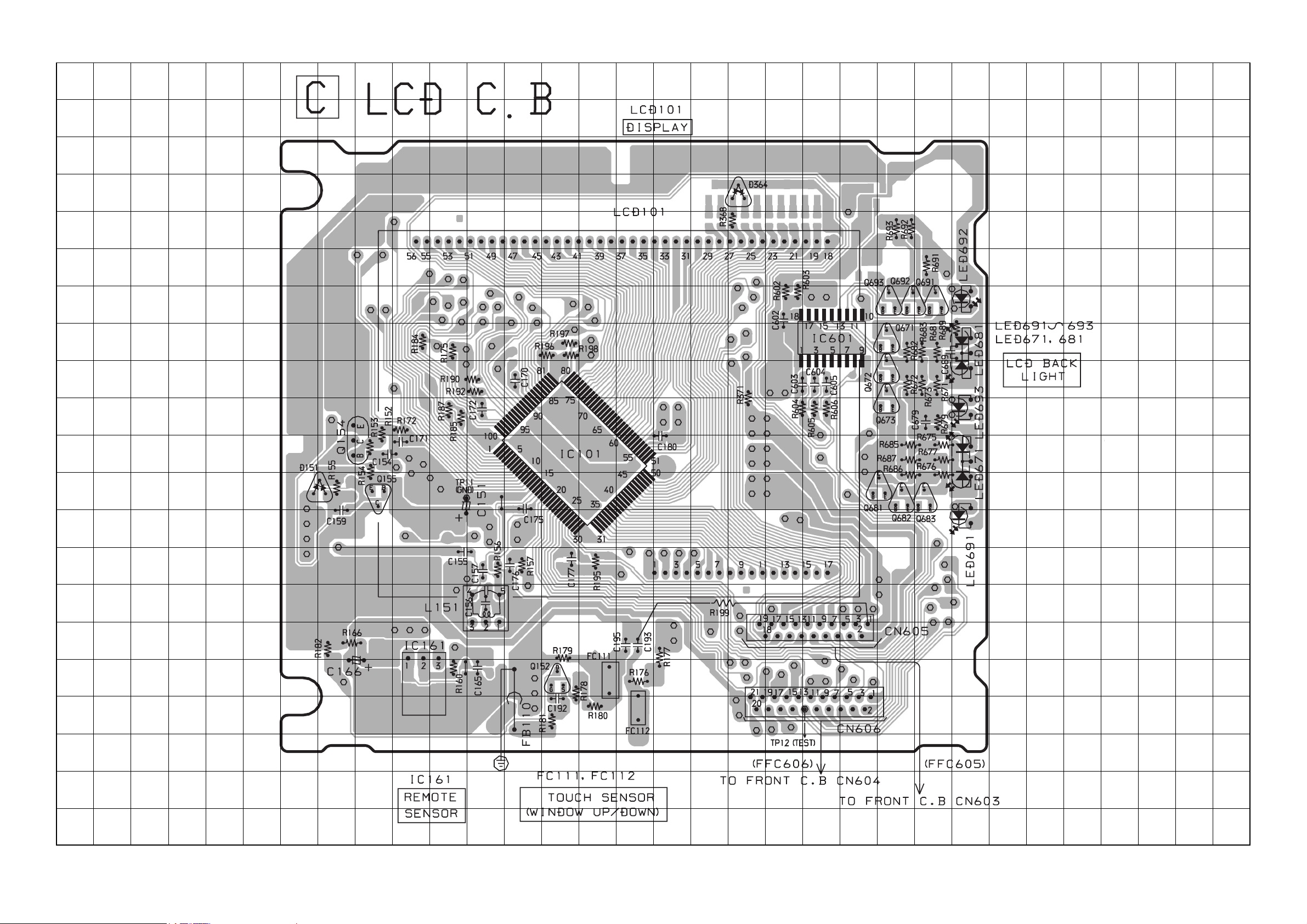
WIRING 4 (LCD) <1 / 2> ................................................................................................................................................ 21
WIRING 4 (LCD) <2 / 2> ................................................................................................................................................22
SCHEMATIC DIAGRAM 5 (LCD) .................................................................................................................................. 23
WIRING 5 (3CH AMP / JACK / DET).............................................................................................................................24
SCHEMATIC DIAGRAM 6 (3CH AMP / JACK / DET)...................................................................................................25
WIRING 6 (PT) ...............................................................................................................................................................26
SCHEMATIC DIAGRAM 7 (PT) .....................................................................................................................................27
WIRING 7 (DSP / FAN / HP / EURO) .............................................................................................................................28
SCHEMATIC DIAGRAM 8 (HP / EURO) .......................................................................................................................29
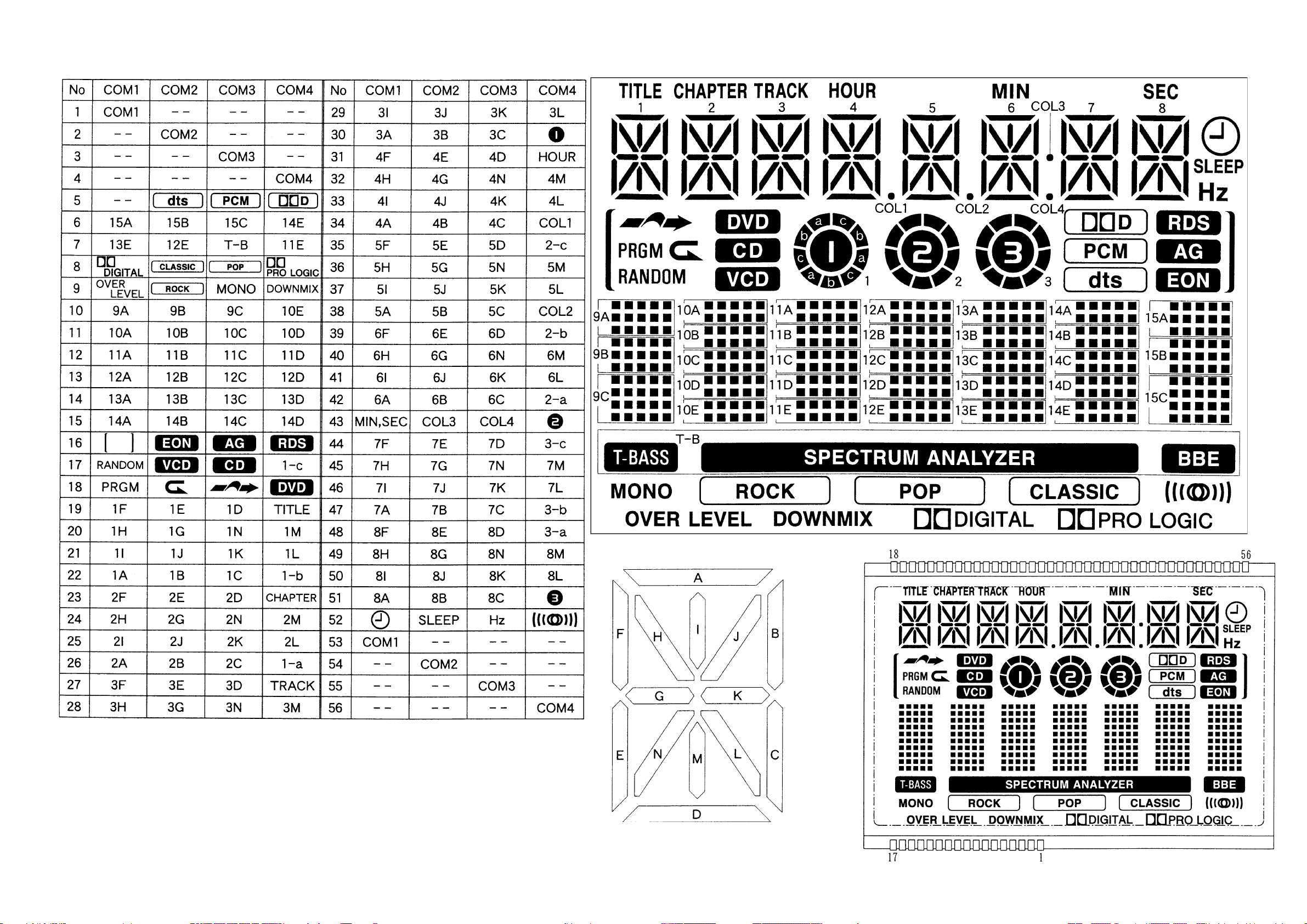
LCD DIAGRAM ......................................................................................................................................................... 30 ~ 32
IC BLOCK DIAGRAM ...............................................................................................................................................33 ~ 34
IC DESCRIPTION ..................................................................................................................................................... 35 ~ 36
ELECTRICAL ADJUSTMENT ................................................................................................................................... 37 ~ 41
DVD TEST MODE ....................................................................................................................................................42 ~ 44
MECHANICAL PARTS ARRANGEMENT ................................................................................................................45 ~ 51
MECHANICAL PARTS LIST 1 / 1 .................................................................................................................................... 52
COLOR NAME TABLE .....................................................................................................................................................52
GENERAL SPEAKER DISASSEMBLY INSTRUCTIONS (FOR REFERENCE) ............................................................ 53
SPEAKER PARTS LIST (SX GDV335) <YSC> ............................................................................................................54
2
Page 3

SPECIFICATIONS
MAIN UNIT CX-GDV335
TUNER
FM tuning range 87.5 MHz to 108 MHz
FM usable sensitivity (IHF)
FM antenna terminal 75 ohms (unbalanced)
MW tuning range 531 kHz to 1602 kHz (9 kHz step)
MW usable sensitivity 350
LW tuning range 144 kHz to 290 kHz
LW usable sensitivity 1400
MW/LW antenna Loop antenna
16.8 dBf
530 kHz to 1710 kHz (10 kHz step)
mV/m
mV/m
AMPLIFIER
Power output Front:
Total harmonic distortion
Input MIC: 1.0 mV (10 kohms)
Output FRONT SPEAKERS: 6 ohms or more
Rated: 60 W + 60 W (6 ohms,
T.H.D. 1 %, 1 kHz/DIN 45500)
Reference: 75 W + 75 W (6 ohms,
T.H.D. 10 %, 1 kHz/DIN 45324)
<EZ only>
DIN MUSIC POWER: 90 W + 90 W
Rear (Surround):
Rated: 20 W + 20 W (8 ohms,
T.H.D. 1 %, 1 kHz/DIN 45500)
Reference: 25 W + 25 W (8 ohms,
T.H.D. 10 %, 1 kHz/DIN 45324)
<EZ only>
DIN MUSIC POWER: 35 W + 35 W
Center:
Rated: 20 W (8 ohms,
T.H.D. 1 %, 1 kHz/DIN 45500)
Reference: 25 W (8 ohms,
T.H.D. 10 %, 1 kHz/DIN 45324)
<EZ only>
DIN MUSIC POWER: 35 W
0.1 % (20 W, 1 kHz, 6 ohms,
DIN AUDIO/Front)
VIDEO/AUX: 300 mV (adjustable)
MD: 300 mV (adjustable)
SURROUND SPEAKERS: 8 ohms to
16 ohms
CENTER SPEAKER: 8 ohms or more
SUB WOOFER: 1 V
LINE OUT: 210 mV
DIGITAL AUDIO OUT (OPTICAL)
PHONES: 32 ohms or more
DISC PLAYER
Laser Semiconductor laser (DVD video discs
Signal-to-noise ratio 90 dB (1 kHz, 0 dB)
Harmonic distortion 0.05 % (1 kHz, 0 dB)
Signal format PAL colour system
S-VIDEO OUT (S1) Y output: 1 Vp-p (75 ohms, unbalanced)
VIDEO OUT Video composite output, 1 Vp-p (75 ohms,
OUT (TV) Video composite output, 1 Vp-p (75 ohms,
Operating conditions 5 °C to 35 °C (41 °F to 95 °F)
l = 650 nm,
C output: 0.286 Vp-p
unbalanced), one RCA jack
unbalanced)
CDs
l = 780 nm)
GENERAL
Power requirements 230 V AC, 50 Hz
Power consumption 210 W
Standby power consumption
Dimensions ( W x H x D) 260 x 266 x 350 mm
Weight 9.8 kg
ECO ON: 0.6 W
ECO OFF: 30 W
FIVE SURROUND SPEAKERS SYSTEM SX-GDV335
(Front, surround and center speakers)
Speaker system 1 way, (magnetic shielded*)
Speaker units 80 mm cone
Impedance Front: 6 ohms
Dimensions (W x H x D) 100 x 220 x 115 mm (with pedestal)
Weight: 0.55 kg
* The surround speakers are not magnetic shielded.
Design and specifications are subject to change without notice.
The word "BBE" and the "BBE symbol" are trademarks of BBE
Sound, Inc.
Under license from BBE Sound,Inc.
Manufactured under license from Dolby Laboratories Licensing
Corporation.
"DOLBY", the double-D symbol and "PRO LOGIC" are
trademarks of Dolby Laboratories Licensing Corporation.
Surround: 8 ohms
Center: 8 ohms
100 x 110 x 115 mm (without pedestal)
ACCESSORIES / PACKAGE LIST
PART NO.
1 8B-DJW-916-110 IB,EZ(ESFGN)I<EZ>
1 8B-DJW-917-110 IB,EZ(ICMP)I<EZ>
1 8B-DJW-915-010 IB,K(E)I<K>
2 87-006-268-010 ANT,LOOP AM
3 87-A90-118-010 ANT,WIRE FM(Z)
4 87-A80-167-010 CORD,PIN 1PY 150CM
!
5 87-099-811-010 PLUG,ADPTR CONV(K)<K>
6 8B-DJW-702-010 RC UNIT,RC-BAS12
NO.
DESCRIPTIONREF. NO. KANRI
Manufactured under license from Digital Theatre Systems, Inc. US
Pat. No. 5,451,942 and other worldwide patents issued and pending.
"DTS" and "DTS Digital Surround" are trademarks of Digital Theatre
Systems Inc. ©1996 Digital Theatre systems, Inc.
All Rights Reserved.
3
Page 4

PROTECTION OF EYES FROM LASER BEAM DURING SERVICING
This set employs laser. Therefore, be sure to follow carefully the
instructions below when servicing.
WARNING!!
WHEN SERVICING, DO NOT APPROACH THE LASER
EXIT WITH THE EYE TOO CLOSELY. IN CASE IT IS
NECESSARY TO CONFIRM LASER BEAM EMISSION.
BE SURE TO OBSERVE FROM A DISTANCE OF MORE
THAN 30cm FROM THE SURFACE OF THE OBJECTIVE
LENS ON THE OPTICAL PICK-UP BLOCK.
Caution: Invisible laser radiation when
open and interlocks defeated avoid
exposure to beam.
Advarsel: Usynlig laserståling ved åbning,
når sikkerhedsafbrydere er ude af funktion.
Undgå udsættelse for stråling.
VAROITUS!
Laiteen Käyttäminen muulla kuin tässä käyttöohjeessa
mainitulla tavalla saataa altistaa käyt-täjän
turvallisuusluokan 1 ylittävälle näkymättömälle
lasersäteilylle.
VARNING!
Om apparaten används på annat sätt än vad som
specificeras i denna bruksanvising, kan användaren
utsättas för osynling laserstrålning, som överskrider
gränsen för laserklass 1.
CAUTION
Use of controls or adjustments or performance of procedures other than those specified herin may result in
hazardous radiation exposure.
ATTENTION
L’utillisation de commandes, réglages ou procédures
autres que ceux spécifiés peut entraîner une dangereuse
exposition aux radiations.
ADVARSEL
Usynlig laserståling ved åbning, når sikkerhedsafbrydereer
ude af funktion. Undgå udsættelse for stråling.
This Compact Disc player is classified as a CLASS 1
LASER product.
The CLASS 1 LASER PRODUCT label is located on the
rear exterior.
CLASS 1 LASER PRODUCT
KLASSE 1 LASER PRODUKT
LUOKAN 1 LASER LAITE
KLASS 1 LASER APPARAT
Precaution to replace Optical block
(SF – HD3AV2)
Body or clothes electrostatic potential could
ruin laser diode in the optical block. Be sure
ground body and workbench, and use care
the clothes do not touch the diode.
1) After the connection, remove solder
shown in the right figure.
PICKUP Assy PWB
Solder short land for
DVD laser diode
Solder short land for
CD laser diode
4
Page 5

NOTE ON BEFORE STARTING REPAIR
1. Forced discharge of electrolytic capacitor of power supply block
When repair is going to be attempted in the set that uses relay circuit in the power supply block, electric potential is kept charged across
the electrolytic capacitors (C101, 102) even though AC power cord is removed. If repair is attempted in this condition, secondary defect
can occur.
In order to prevent the secondary trouble, perform the following measures before starting repair work.
Discharge procedure
11
1 Remove the AC power cord.
11
22
2 Connect a discharging resistor at an end of lead wire that
22
has clips at both ends. Connect the other end of the lead
wire to metal chassis.
33
3 Contact the other end of the discharging resistor to the
33
positive (+) side (+VH) of C101. (For two seconds)
44
4 Contact the same end of the discharging resistor as step
44
33
3 to the negative (-) side (-VH) of C102 in the same way.
33
(For two seconds)
55
5 Check that voltage across C101 and C102 has decreased
55
to 1 V or less using a multimeter or an oscilloscope.
Select a discharging resistor referring to the following table.
Charging voltage (V) Discharging
(C101, 102) resistor (Ω)
25-48 100 3 87-A00-247-090
49-140 220 5 87-A00-232-090
Note: The reference numbers (C101, C102) of the electrolytic capacitors can change depending on the models. Be sure to check the
reference numbers of the charging capacitors on schematic diagram before starting the discharging work.
Rated power (W) Parts number
MAIN C.B
D101
3
C101 C102
22
Fig-1
4
2. Check items before exchanging the MICROCOMPUTER
Be sure to check the following items before exchanging the MICROCOMPUTER. Exchange the MICROCOMPUTER after confirming
that the MICROCOMPUTER is surely defective.
2-1. Regarding the HOLD terminal of the MICROCOMPUTER
When the HOLD terminal (INPUT) of the MICROCOMPUTER is “H”, the MICROCOMPUTER is judged to be operating correctly.
When this terminal is “L”, the main power cannot be turned on. Therefore, be sure to check the terminal voltage of the HOLD
terminal before exchange.
When the MICROCOMPUTER is not defective, the HOLD terminal can also go “L” when the POWER AMPLIFIER has any
abnormalities that triggers the abnormality detection circuit on the MAIN C. B. that sets the HOLD terminal to “L”.
• Good or no good judgement of the MICROCOMPUTER
11
1 Turn on the AC main power.
11
22
2 Confirm that the main power is turned on and the HOLD terminal of the MICROCOMPUTER keeps the “H” level or not.
22
33
3 When the HOLD terminal is “L” level, the abnormality detection circuit is judged to be working correctly and the
33
MICROCOMPUTER is judged to be good.
– 5 –
Page 6

In such a case, check also if the POWER AMPLIFIER circuit or power supply circuit has any abnormalities or not.
2-2. Regarding reset
There are cases that the machine does not work correctly because the MICROCOMPUTER is not reset even though the AC power
cord is re-inserted, or the software reset (pressing the STOP key + POWER key) is performed.
When the above described phenomenon occurs, it can lead to wrong judgement as if the MICROCOMPUTER is defective and to
exchange the MICROCOMPUTER. In such a case, perform the forced-reset by the following procedure and check good or no
good of the MICROCOMPUTER.
11
1 Remove the AC power cord.
11
FRONT C.B
18
MICROCOMPUTER
FRONT C.B
22
2 Short both ends of the electrolytic capacitor C113 that is connected to VDD of the MICROCOMPUTER with tweezers.
22
33
3 Connect the AC power cord again. If the MICROCOMPUTER returns to the normal operation, the MICROCOMPUTER is
33
good.
Note: The reference number or MICROCOMPUTER pin number of transistor (Q110) and electrolytic capacitor (C113) can change depending
on the models. Be sure to check the reference numbers on schematic diagram before starting the discharging work.
15
C113
Short with tweezers.
Fig-2-2
C113
%
*
VSS
VDD
MICROCOMPUTER
2-3. Confirmation of soldering state of MICROCOMPUTER
Check the soldering state of the MICROCOMPUTER in addition to the above described procedures. Be sure to exchange the
MICROCOMPUTER after surely confirming that the trouble is not caused by poor soldering but the MICROCOMPUTER itself.
– 6 –
Page 7

DISASSEMBLY INSTRUCTIONS
Assembling HLDR MECHA ASSY
1. Join the PLATE MAIN CAM to the HLDR MECHA ASSY as shown in the pictures below:
HLDR MECHA ASSY
PLATE CAM
SECOND
2. Join the HLDR MECHA ASSY to the FRONT portion, keeping the main unit DISPLAY portion lower.
FRONT
DISPLAY
* Adjusting phases is not required in HLDR MECHA ASSY.
– 7 –
Page 8

ELECTRICAL MAIN PARTS LIST
PART NO. DESCRIPTIONREF. NO. KANRI
NO.
IC
8B-DJW-621-030 C-IC,LC877256V-5W18
87-A21-831-010 IC,SPS-422-1-F1
87-A21-018-040 C-IC,M65849BFP631D
87-070-289-040 C-IC,BU2092F
87-A21-882-030 C-IC,M62466FP
87-A21-021-040 C-IC,BU2099FV
87-A21-023-040 C-IC,BA3835F
87-A21-695-010 IC,LA1845L
87-A20-440-040 C-IC,BU1920FS
87-A21-928-010 IC,LC72131D-N
TRANSISTOR
87-A30-559-010 TR,CSB1370EF
87-026-610-080 TR,KTC3198GR
87-A30-076-080 C-TR,2SC3052F
87-A30-075-080 C-TR,2SA1235F
87-A30-495-080 TR,2SA1981Y
87-A30-257-080 C-TR,2SD1306E
87-A30-636-040 C-TR,SBT5551F
87-A30-190-080 TR,CC5551
87-A30-086-040 C-TR,CSD1306E
87-A30-256-010 TR,2SD1933
87-A30-255-010 TR,2SB1342
87-A30-635-040 C-TR,SBT5401F
87-A30-494-080 TR,2SA1980G
87-A30-087-080 C-FET,2SK2158
87-A30-490-080 C-TR,KRC107S
87-A30-047-080 TR,CSD655E
87-A30-074-080 C-TR,RT1P 141C
87-A30-484-080 C-TR,KRA102S
87-A30-071-080 C-TR,RT1N 144C
87-A30-529-010 TR,2SD2642
87-A30-528-010 TR,2SB1686
87-A30-162-010 FET,2SK2937
87-A30-520-080 TR,2SC5342Y
87-A30-515-080 TR,2SA1979O/Y
87-A30-086-070 C-TR,CSD1306E
87-A30-063-080 C-TR,KRA104S
89-327-143-080 C-TR,2SC2714O
87-A30-489-080 C-TR,KRA107S
89-503-602-080 C-FET,2SK360E
87-A30-234-080 TR,CSC4115BC
DIODE
87-A40-291-080 DIODE,1N4148(CPT)
87-A40-839-090 DIODE,G5SBA60L-6088
87-A40-838-090 DIODE,G3SBA60L-6088
87-A40-764-080 ZENER,UZ10BSC
87-A40-553-080 DIODE,1N4003 LES
87-A40-270-080 C-DIODE,MC2838
87-A40-269-080 C-DIODE,MC2836
87-A40-488-080 DIODE,1SS244
87-A40-748-080 ZENER,UZ5.6BSA
87-A40-749-080 ZENER,UZ5.6BSB
87-A40-747-080 ZENER,UZ5.1BSB
87-A40-393-090 DIODE,1N5402GW(F20)
87-A40-745-080 ZENER,UZ4.7BSA
87-017-149-080 ZENER,HZS6A2L
MAIN C.B
C5 87-012-368-080 C-CAP,S 0.1-50 F
C6 87-012-368-080 C-CAP,S 0.1-50 F
C7 87-012-368-080 C-CAP,S 0.1-50 F
C8 87-012-368-080 C-CAP,S 0.1-50 F
C9 87-012-368-080 C-CAP,S 0.1-50 F
C10 87-012-368-080 C-CAP,S 0.1-50 F
DESCRIPTIONREF. NO. KANRI
PART NO.
NO.
C11 87-012-368-080 C-CAP,S 0.1-50 F
C12 87-012-368-080 C-CAP,S 0.1-50 F
C21 87-A12-780-090 CAP,E 4700-35 M 85 SKR
C22 87-A12-780-090 CAP,E 4700-35 M 85 SKR
C23 87-A12-779-090 CAP,E 3300-50 M 85 SKR
C24 87-A12-779-090 CAP,E 3300-50 M 85 SKR
C32 87-012-286-080 CAP,U 0.01-25
C34 87-A12-095-080 CAP,E 100-50 SMG
C35 87-A12-076-080 CAP,E 22-35 SMG
C36 87-A12-068-080 CAP,E 470-16 SMG
C40 87-012-286-080 CAP,U 0.01-25
C41 87-A10-831-080 CAP,E 1000-25 M SMG
C60 87-A12-089-080 CAP,E 3.3-50 SMG
C63 87-A12-071-080 CAP,E 47-25 SMG
C81 87-A10-918-080 CAP,E 100-16 SMG
C101 87-A12-090-080 CAP,E 4.7-50 SMG
C102 87-A12-090-080 CAP,E 4.7-50 SMG
C111 87-010-495-040 CAP,E 2.2-50 GAS
C112 87-010-495-040 CAP,E 2.2-50 GAS
C113 87-A12-075-080 CAP,E 10-35 SMG
C114 87-A12-091-080 CAP,E 10-50 SMG
C121 87-010-495-040 CAP,E 2.2-50 GAS
C122 87-010-493-040 CAP,E 0.47-50 GAS
C141 87-010-191-080 C-CAP,S 0.015-50 F
C142 87-010-191-080 C-CAP,S 0.015-50 F
C145 87-012-368-080 C-CAP,S 0.1-50 F
C146 87-012-368-080 C-CAP,S 0.1-50 F
C147 87-012-368-080 C-CAP,S 0.1-50 F
C148 87-012-368-080 C-CAP,S 0.1-50 F
C149 87-010-190-080 S CHIP F,0.01
C150 87-010-190-080 S CHIP F,0.01
C156 87-012-274-080 CHIP CAP,U 1000P-50B
C170 87-012-278-080 C-CAP,U 2200P-50 B
C171 87-012-282-080 CAP,U 4700P-50
C173 87-010-759-080 C-CAP,U 0.1-25F
C201 87-012-281-080 C-CAP,U 3900P-50 B
C202 87-012-281-080 C-CAP,U 3900P-50 B
C203 87-A12-085-080 CAP,E 0.33-50 SMG
C204 87-A12-085-080 CAP,E 0.33-50 SMG
C205 87-012-282-080 CAP,U 4700P-50
C206 87-012-282-080 CAP,U 4700P-50
C207 87-A12-090-080 CAP,E 4.7-50 SMG
C208 87-A12-090-080 CAP,E 4.7-50 SMG
C209 87-016-615-080 C-CAP,U 2.2P-50CH
C210 87-016-615-080 C-CAP,U 2.2P-50CH
C211 87-A12-078-080 CAP,E 47-35 SMG
C212 87-A12-078-080 CAP,E 47-35 SMG
C215 87-012-273-080 C-CAP,U 820P-50 B
C216 87-012-273-080 C-CAP,U 820P-50 B
C217 87-A10-596-080 C-CAP,S 100P-100 J CH
C218 87-A10-596-080 C-CAP,S 100P-100 J CH
C219 87-012-368-080 C-CAP,S 0.1-50 F
C220 87-012-368-080 C-CAP,S 0.1-50 F
C221 87-012-286-080 CAP,U 0.01-25
C222 87-012-286-080 CAP,U 0.01-25
C223 87-A10-596-080 C-CAP,S 100P-100 J CH
C224 87-A10-596-080 C-CAP,S 100P-100 J CH
C273 87-010-759-080 C-CAP,U 0.1-25F
C274 87-A12-091-080 CAP,E 10-50 SMG
C275 87-A12-091-080 CAP,E 10-50 SMG
C580 87-016-369-080 C-CAP,S 0.033-25 B K
C581 87-012-199-080 CAP,220P
C582 87-012-274-080 CHIP CAP,U 1000P-50B
C583 87-010-759-080 C-CAP,U 0.1-25F
C584 87-012-274-080 CHIP CAP,U 1000P-50B
C585 87-010-759-080 C-CAP,U 0.1-25F
C586 87-010-405-010 CAP,E 10-50 SME
C603 87-010-319-080 C-CAP,S 56P-50 JCH
C604 87-010-319-080 C-CAP,S 56P-50 JCH
C607 87-010-319-080 C-CAP,S 56P-50 JCH
8
Page 9

PART NO. DESCRIPTIONREF. NO. KANRI
NO.
C608 87-010-319-080 C-CAP,S 56P-50 JCH
C619 87-012-368-080 C-CAP,S 0.1-50 ZF
C620 87-010-260-080 CAP,ELECT 47-25V
C633 87-012-281-080 C-CAP,U 3900P-50 B
C634 87-016-369-080 C-CAP,S 0.033-25 B K
C635 87-012-281-080 C-CAP,U 3900P-50 B
C636 87-016-369-080 C-CAP,S 0.033-25 B K
C637 87-A12-088-080 CAP,E 2.2-50 SMG
C638 87-A12-088-080 CAP,E 2.2-50 SMG
C639 87-A12-088-080 CAP,E 2.2-50 SMG
C640 87-A12-088-080 CAP,E 2.2-50 SMG
C641 87-012-280-080 CAP,U 3300P-50
C642 87-010-757-080 C-CAP,U 0.047-25F
C643 87-016-114-080 C-CAP,U 0.01-25B
C644 87-016-114-080 C-CAP,U 0.01-25B
C645 87-016-114-080 C-CAP,U 0.01-25B
C646 87-016-114-080 C-CAP,U 0.01-25B
C647 87-A12-309-080 C-CAP,U 680P-50 J CH
C648 87-A12-309-080 C-CAP,U 680P-50 J CH
C649 87-A10-260-080 C-CAP,U 0.1-16 K B
C650 87-016-118-080 C-CAP,U 0.022-25BJ
C651 87-016-118-080 C-CAP,U 0.022-25BJ
C652 87-A10-260-080 C-CAP,U 0.1-16 K B
C653 87-A10-260-080 C-CAP,U 0.1-16 K B
C654 87-016-397-080 C-CAP,U 0.047-16BJ
C655 87-016-397-080 C-CAP,U 0.047-16BJ
C656 87-A10-260-080 C-CAP,U 0.1-16 K B
C657 87-016-460-080 C-CAP,S 0.22-16 B
C658 87-016-460-080 C-CAP,S 0.22-16 B
C659 87-016-469-080 CAP,E 6.8-50 5L
C660 87-A12-090-080 CAP,E 4.7-50 SMG
C661 87-016-460-080 C-CAP,S 0.22-16 B
C662 87-016-460-080 C-CAP,S 0.22-16 B
C663 87-A10-799-080 C-CAP,S 5600P-16 J B CM
C664 87-016-397-080 C-CAP,U 0.047-16BJ
C665 87-A10-230-080 C-CAP,S 0.68-25 Z F
C666 87-A11-183-080 C-CAP,S 0.12-16 J B
C667 87-010-560-040 CAP,E 10-50 GAS
C668 87-010-560-040 CAP,E 10-50 GAS
C669 87-010-494-040 CAP,E 1-50 GAS
C670 87-010-494-040 CAP,E 1-50 GAS
C675 87-012-282-080 CAP,U 4700P-50
C676 87-012-282-080 CAP,U 4700P-50
C683 87-010-189-080 C-CAP,S 8200P-50 B
C684 87-A12-075-080 CAP,E 10-35 SMG
C685 87-012-167-080 C-CAP,U 5P-50 CH
C686 87-010-759-080 C-CAP,U 0.1-25F
C687 87-010-759-080 C-CAP,U 0.1-25F
C688 87-A12-062-080 CAP,E 100-10 SMG
C689 87-A12-058-080 CAP,E 470-6.3 SMG
C701 87-012-195-080 C-CAP,U 100P-50CH
C702 87-012-195-080 C-CAP,U 100P-50CH
C703 87-012-286-080 CAP,U 0.01-25
C707 87-A12-088-080 CAP,E 2.2-50 SMG
C708 87-A12-088-080 CAP,E 2.2-50 SMG
C771 87-A12-062-080 CAP,E 100-10 SMG
C772 87-012-286-080 CAP,U 0.01-25
C779 87-010-180-080 C-CER,1500P
C780 87-010-180-080 C-CER,1500P
C782 87-012-286-080 CAP,U 0.01-25
C783 87-012-286-080 CAP,U 0.01-25
C784 87-012-286-080 CAP,U 0.01-25
C785 87-012-286-080 CAP,U 0.01-25
C786 87-012-286-080 CAP,U 0.01-25
C788 87-012-167-080 C-CAP,U 5P-50 CH
C789 87-016-118-080 C-CAP,U 0.022-25BJ
C790 87-016-118-080 C-CAP,U 0.022-25BJ
C791 87-010-831-080 C-CAP,U 0.1-16F
C792 87-012-286-080 CAP,U 0.01-25
C793 87-A12-090-080 CAP,E 4.7-50 SMG
DESCRIPTIONREF. NO. KANRI
PART NO.
NO.
C795 87-012-286-080 CAP,U 0.01-25
C796 87-012-286-080 CAP,U 0.01-25
C797 87-A12-091-080 CAP,E 10-50 SMG
C798 87-012-286-080 CAP,U 0.01-25
C799 87-A12-065-080 CAP,E 33-16 SMG
C800 87-010-829-080 CAP,U 0.047-16
C801 87-A12-089-080 CAP,E 3.3-50 SMG
C802 87-010-829-080 CAP,U 0.047-16
C803 87-010-787-080 CAP,U 0.022-25
C804 87-A12-062-080 CAP,E 100-10 SMG
C807 87-A12-086-080 CAP,E 0.47-50 SMG
C808 87-A12-087-080 CAP,E 1-50 SMG
C809 87-A12-087-080 CAP,E 1-50 SMG
C810 87-010-831-080 C-CAP,U 0.1-16F
C814 87-012-286-080 CAP,U 0.01-25
C815 87-A12-086-080 CAP,E 0.47-50 SMG
C816 87-A12-086-080 CAP,E 0.47-50 SMG
C818 87-012-276-080 CAP,CHIP SS 1500P PBK
C821 87-A12-091-080 CAP,E 10-50 SMG
C823 87-A10-915-080 C-CAP,U 1000P-25 J CH
C824 87-A12-090-080 CAP,E 4.7-50 SMG
C825 87-010-596-080 CAP,S 0.047-16
C831 87-A12-092-080 CAP,E 22-50 SMG
C842 87-012-286-080 CAP,U 0.01-25
C843 87-012-286-080 CAP,U 0.01-25
C844 87-012-286-080 CAP,U 0.01-25
C845 87-012-286-080 CAP,U 0.01-25
C846 87-012-286-080 CAP,U 0.01-25
C847 87-010-197-080 CAP,CHIP 0.01 DM
C848 87-010-197-080 CAP,CHIP 0.01 DM
C849 87-012-286-080 CAP,U 0.01-25
C850 87-A12-071-080 CAP,E 47-25 SMG
C851 87-012-286-080 CAP,U 0.01-25
C852 87-012-286-080 CAP,U 0.01-25
C853 87-012-286-080 CAP,U 0.01-25
C858 87-010-831-080 C-CAP,U 0.1-16F
C859 87-010-831-080 C-CAP,U 0.1-16F
C860 87-012-286-080 CAP,U 0.01-25
C869 87-012-286-080 CAP,U 0.01-25
C870 87-012-274-080 CHIP CAP,U 1000P-50B
C871 87-012-199-080 CAP,220P
C872 87-012-199-080 CAP,220P
C873 87-A10-039-080 C-CAP,U 470P-50 J CH
C874 87-A12-091-080 CAP,E 10-50 SMG
C875 87-010-759-080 C-CAP,U 0.1-25F
C876 87-A12-091-080 CAP,E 10-50 SMG
C877 87-012-286-080 CAP,U 0.01-25
C878 87-012-184-080 C-CAP,U 33P-50 CH
C879 87-012-180-080 C-CAP,U 22P-50 CH
C940 87-012-286-080 CAP,U 0.01-25
C942 87-012-165-080 C-CAP,U 3P-50 C CH
C947 87-012-286-080 CAP,U 0.01-25
C948 87-A10-039-080 C-CAP,U 470P-50 J CH
C952 87-012-286-080 CAP,U 0.01-25
C957 87-012-174-080 CAP,CHIP CERA SS 12P CHJ
C958 87-012-286-080 CAP,U 0.01-25
C959 87-010-831-080 C-CAP,U 0.1-16F
C960 87-010-831-080 C-CAP,U 0.1-16F
C962 87-A12-087-080 CAP,E 1-50 SMG
C963 87-015-785-080 CHIP CAPACITOR,0.1FZ-25Z
C971 87-A12-067-080 CAP,E 330-16 SMG
C972 87-A12-090-080 CAP,E 4.7-50 SMG
C973 87-012-286-080 CAP,U 0.01-25
C974 87-012-286-080 CAP,U 0.01-25
C979 87-012-195-080 C-CAP,U 100P-50CH
C981 87-A12-071-080 CAP,E 47-25 SMG
C982 87-010-831-080 C-CAP,U 0.1-16F
C983 87-012-286-080 CAP,U 0.01-25
C984 87-012-286-080 CAP,U 0.01-25
C985 87-012-195-080 C-CAP,U 100P-50CH
9
Page 10

PART NO. DESCRIPTIONREF. NO. KANRI
NO.
C987 87-012-286-080 CAP,U 0.01-25
C989 87-012-286-080 CAP,U 0.01-25
C991 87-012-176-080 CAP,15P
C992 87-012-176-080 CAP,15P
C993 87-012-274-080 CHIP CAP,U 1000P-50B
C995 87-012-274-080 CHIP CAP,U 1000P-50B
C997 87-010-831-080 C-CAP,U 0.1-16F
C998 87-A12-071-080 CAP,E 47-25 SMG
C999 87-A11-155-080 CAP,TC U 0.01-16 Z F
CF831 87-008-423-010 FLTR,CF SFE10.7MS3G-A
CF832 82-785-747-010 CF,MS2 GHY R
CN105 87-099-196-010 CONN,8P 6216 V
CN183 87-099-564-010 CONN,4P TUC-P4P-B1
CN551 87-099-668-010 CONN,9P TUC-P 9P-B1
CN601 87-099-719-010 CONN,30P TYK-B(X)
CN603 87-099-013-010 CONN,11P 6216 V
CN605 87-A61-109-010 CONN,7P V TID-A
CN701 87-099-197-010 CONN,9P 6216 V
CNA1 8A-NF6-646-010 CONN ASSY,9P TID-A(460)
CNA102 8B-DJW-630-010 CONN ASSY,7P TID-A(150)
FFC105 88-908-301-110 FF-CABLE,8P 1.25
FFC603 88-911-511-110 FF-CABLE,11P 1.25 510MM
FFC701 88-909-511-110 FF-CABLE,9P 1.25 510MM
FFE831 A8-6ZA-19C-170 6ZA-1 YFEENC
J102 87-A60-238-010 TERMINAL,SP 4P(MSC)
J601 87-A60-885-010 JACK,PIN 6P R/W MSC
J832 87-A60-403-010 TERMINAL,ANT PAL 2P HSP-312V05
L141 87-A50-610-010 COIL,1UH K(MDEC)
L142 87-A50-610-010 COIL,1UH K(MDEC)
L801 87-A50-608-010 COIL,FM DET-N(TOK)
L802 87-A91-551-010 FLTR,PCFJZH-450 L(TOK)
L811 87-005-847-080 COIL,2.2UH(CECS)
L832 87-005-847-080 COIL,2.2UH(CECS)
L861 87-005-847-080 COIL,2.2UH(CECS)
L941 87-A50-020-010 COIL,ANT LW(COI)252KHZ
L942 87-A50-019-010 COIL,OSC LW(COI)856KHZ
L951 8A-NF8-668-010 COIL,AM PACK 2(TOK)
R85 87-A00-436-050 RES,100-1/2W J RP
R86 87-A00-436-050 RES,100-1/2W J RP
R87 87-A00-436-050 RES,100-1/2W J RP
R88 87-A00-436-050 RES,100-1/2W J RP
R255 87-A00-262-080 RES,M/F 0.15-2W J
R256 87-A00-262-080 RES,M/F 0.15-2W J
R259 87-A00-262-080 RES,M/F 0.15-2W J
R260 87-A00-262-080 RES,M/F 0.15-2W J
R681 87-010-992-080 C-CAP,S 0.047-25 B
R682 87-010-992-080 C-CAP,S 0.047-25 B
R790 87-012-286-080 CAP,U 0.01-25
R991 87-012-195-080 C-CAP,U 100P-50CH
R993 87-012-195-080 C-CAP,U 100P-50CH
R995 87-012-195-080 C-CAP,U 100P-50CH
TC942 87-A91-774-080 TRIMMER,PLY 30P 6.8X5.4 CDYL
TH201 87-A91-042-080 C-THMS,100K 55001
TH202 87-A91-042-080 C-THMS,100K 55001
WH1 87-A90-510-010 HLDR,WIRE 2.5-9P
WH102 87-A90-460-010 HLDR,WIRE 2.5-7P
X861 87-A70-307-010 VIB,XTAL 4.332MHZ CSA-309ST
X991 87-A70-306-010 VIB,XTAL 4.500MHZ CSA-309ST
FRONT C.B
C141 87-012-278-080 C-CAP,U 2200P-50 B
C190 87-012-271-080 CAP,U 560P-50
C191 87-012-195-080 C-CAP,U 100P-50CH
C193 87-012-271-080 CAP,U 560P-50
C194 87-012-195-080 C-CAP,U 100P-50CH
C315 87-010-759-080 C-CAP,U 0.1-25F
C441 87-010-412-040 CAP,E 10-25 5L
C621 87-010-405-040 CAP,E 10-50
C622 87-010-759-080 C-CAP,U 0.1-25F
DESCRIPTIONREF. NO. KANRI
PART NO.
NO.
C623 87-012-188-080 C-CAP,U 47P-50 CH
C624 87-012-188-080 C-CAP,U 47P-50 CH
C625 87-012-188-080 C-CAP,U 47P-50 CH
C703 87-010-759-080 C-CAP,U 0.1-25F
C704 87-010-759-080 C-CAP,U 0.1-25F
C705 87-010-759-080 C-CAP,U 0.1-25F
C706 87-010-759-080 C-CAP,U 0.1-25F
C707 87-010-759-080 C-CAP,U 0.1-25F
CN101 87-099-720-010 CONN,30P TYK-B(P)
CN103 87-099-201-010 CONN,8P 6216 H
CN141 87-A60-667-010 CONN,3P H 2MM JMT
CN401 87-099-212-010 CONN,5P 6216 V
CN502 87-099-212-010 CONN,5P 6216 V
CN603 87-A61-361-010 CONN,19P V GRY FMN-BTK
CN604 87-A61-385-010 CONN,21P H GRY FMN-SSTK
FFC103 88-908-381-110 FF-CABLE,8P 1.25
FFC401 88-905-281-110 FF-CABLE,5P 1.25 280MM
FFC502 88-905-361-110 FF-CABLE,5P 1.25 360MM
LED140 87-A40-266-080 LED,SLH-56VCT31 RED
LED672 87-A40-809-040 LED,LTL-307KK PGRN
LED673 87-A40-809-040 LED,LTL-307KK PGRN
LED674 87-A40-809-040 LED,LTL-307KK PGRN
LED675 87-A40-809-040 LED,LTL-307KK PGRN
LED676 87-A40-809-040 LED,LTL-307KK PGRN
LED677 87-A40-809-040 LED,LTL-307KK PGRN
S301 87-A90-095-080 SW,TACT EVQ11G04M
S302 87-A90-095-080 SW,TACT EVQ11G04M
S303 87-A90-095-080 SW,TACT EVQ11G04M
S304 87-A90-095-080 SW,TACT EVQ11G04M
SW162 87-A92-249-010 SW,RTRY EC12E24704-30MM
SW163 87-A92-113-010 SW,RTRY EC12E12504 30MM
X201 87-XMN-602-010 VIB,PIEZO PKM13EPY
LCD C.B
C151 87-A10-189-040 CAP,E 220-10
C154 87-A10-592-080 C-CAP,S 0.015-50 J B
C155 87-012-176-080 CAP,15P
C156 87-012-195-080 C-CAP,U 100P-50CH
C157 87-012-198-080 CAP,180P
C159 87-A10-353-080 C-CAP,U 0.22-10KB
C165 87-012-336-080 CAP,CHIP SS 330P SL
C166 87-010-075-040 CAP,E 10-16 5L
C170 87-010-759-080 C-CAP,U 0.1-25F
C171 87-016-114-080 C-CAP,U 0.01-25B
C172 87-010-759-080 C-CAP,U 0.1-25F
C175 87-010-759-080 C-CAP,U 0.1-25F
C176 87-012-274-080 CHIP CAP,U 1000P-50B
C177 87-010-194-080 CAP,CHIP 0.047
C180 87-010-759-080 C-CAP,U 0.1-25F
C192 87-012-172-080 C-CAP,U 10P-50 D CH
C193 87-018-209-080 CAP,CER 0.1-50V
C195 87-A10-207-080 CAP,TC U 0.01-50 KB
C602 87-010-759-080 C-CAP,U 0.1-25F
C603 87-012-188-080 C-CAP,U 47P-50 CH
C604 87-012-188-080 C-CAP,U 47P-50 CH
C605 87-012-188-080 C-CAP,U 47P-50 CH
C679 87-010-759-080 C-CAP,U 0.1-25F
C689 87-010-759-080 C-CAP,U 0.1-25F
CN605 87-A61-361-010 CONN,19P V GRY FMN-BTK
CN606 87-A61-090-010 CONN,21P V GRY FMN-BTK
FB110 87-008-372-080 FILTER,EMI BLO1RN1
FC111 87-033-213-080 FUSE CLAMP,PFC5000
FC112 87-033-213-080 FUSE CLAMP,PFC5000
FFC605 8B-DJW-632-010 FF-CABLE,19P 1.0 220MM
FFC606 8B-DJW-631-010 FF-CABLE,21P 1.0 180MM
L151 87-A50-657-010 COIL,CLK 9.43MHZ(TOKO)7KLY
LCD101 8B-DJW-616-110 LCD,AIW4279-30P1N
LED671 87-A92-077-010 LED,SMLU1BE16C-SLF73 BLU/UMB
LED681 87-A92-077-010 LED,SMLU1BE16C-SLF73 BLU/UMB
10
Page 11

PART NO. DESCRIPTIONREF. NO. KANRI
!
!
!!!
!
DESCRIPTIONREF. NO. KANRI
NO.
LED691 87-A92-078-010 LED,SELU1D10CXM-SLF38 GR
LED692 87-A92-078-010 LED,SELU1D10CXM-SLF38 GR
LED693 87-A92-078-010 LED,SELU1D10CXM-SLF38 GR
3CH AMP C.B
C101 87-012-278-080 C-CAP,U 2200P-50 B
C102 87-012-278-080 C-CAP,U 2200P-50 B
C103 87-A12-087-080 CAP,E 1-50 SMG
C104 87-A12-087-080 CAP,E 1-50 SMG
C107 87-A12-095-080 CAP,E 100-50 SMG
C108 87-A12-095-080 CAP,E 100-50 SMG
C111 87-A12-078-080 CAP,E 47-35 SMG
C112 87-A12-078-080 CAP,E 47-35 SMG
C113 87-012-195-080 C-CAP,U 100P-50CH
C114 87-012-195-080 C-CAP,U 100P-50CH
C117 87-A10-596-080 C-CAP,S 100P-100 J CH
C118 87-A10-596-080 C-CAP,S 100P-100 J CH
C119 87-012-368-080 C-CAP,S 0.1-50 F
C120 87-012-368-080 C-CAP,S 0.1-50 F
C121 87-012-286-080 CAP,U 0.01-25
C122 87-012-286-080 CAP,U 0.01-25
C125 87-010-831-080 C-CAP,U 0.1-16F
C201 87-012-278-080 C-CAP,U 2200P-50 B
C202 87-A12-087-080 CAP,E 1-50 SMG
C204 87-A12-095-080 CAP,E 100-50 SMG
C206 87-A12-078-080 CAP,E 47-35 SMG
C207 87-012-195-080 C-CAP,U 100P-50CH
C209 87-A10-596-080 C-CAP,S 100P-100 J CH
C210 87-012-368-080 C-CAP,S 0.1-50 F
C211 87-012-286-080 CAP,U 0.01-25
C300 87-012-278-080 C-CAP,U 2200P-50 B
C301 87-012-282-080 CAP,U 4700P-50
CN102 87-A61-109-010 CONN,7P V TID-A
CN103 87-A60-059-010 CONN,08P V 9604S-08C
R157 87-A00-258-080 RES,M/F 0.22-1W J
R158 87-A00-258-080 RES,M/F 0.22-1W J
R161 87-A00-258-080 RES,M/F 0.22-1W J
R162 87-A00-258-080 RES,M/F 0.22-1W J
R230 87-A00-258-080 RES,M/F 0.22-1W J
R231 87-A00-258-080 RES,M/F 0.22-1W J
TH101 87-A91-042-080 C-THMS,100K 55001
TH102 87-A91-042-080 C-THMS,100K 55001
TH201 87-A91-042-080 C-THMS,100K 55001
W201 8B-DJW-629-010 F-CABLE,6P 2.5 220MM
KEY C.B
CNA3 88-803-033-010 CONN ASSY,3P 300MM
S321 87-A90-095-080 SW,TACT EVQ11G04M
S322 87-A90-095-080 SW,TACT EVQ11G04M
S323 87-A90-095-080 SW,TACT EVQ11G04M
S324 87-A90-095-080 SW,TACT EVQ11G04M
S325 87-A90-095-080 SW,TACT EVQ11G04M
S326 87-A90-095-080 SW,TACT EVQ11G04M
S327 87-A90-095-080 SW,TACT EVQ11G04M
S328 87-A90-095-080 SW,TACT EVQ11G04M
S341 87-A90-095-080 SW,TACT EVQ11G04M
S342 87-A90-095-080 SW,TACT EVQ11G04M
S343 87-A90-095-080 SW,TACT EVQ11G04M
S344 87-A90-095-080 SW,TACT EVQ11G04M
S345 87-A90-095-080 SW,TACT EVQ11G04M
S346 87-A90-095-080 SW,TACT EVQ11G04M
S347 87-A90-095-080 SW,TACT EVQ11G04M
S348 87-A90-095-080 SW,TACT EVQ11G04M
S349 87-A90-095-080 SW,TACT EVQ11G04M
S350 87-A90-095-080 SW,TACT EVQ11G04M
S351 87-A90-095-080 SW,TACT EVQ11G04M
S352 87-A90-095-080 SW,TACT EVQ11G04M
PART NO.
NO.
PT C.B
C1 87-018-209-080 CAP,CER 0.1-50V
CN1 87-A61-110-010 CONN,9P V TID-A
FB1 87-A90-457-010 F-BEAD,15-25-15 E2515 JRT
PT1 8B-DJW-624-010 PT,BDJ-29EZ
PT2 8B-MA6-675-010 PT,SUB BMA E (VRK)
RY2 87-A91-418-010 RELAY,AC12V G5PA-1-M
T1 87-A60-317-010 TERMINAL,1P MSC
T2 87-A60-317-010 TERMINAL,1P MSC
MIC C.B
C502 87-010-186-080 CAP,CHIP 4700P
C503 87-010-112-040 CAP,E 100-16
C504 87-010-405-040 CAP,E 10-50
C506 87-010-320-080 CHIP CAP,68P
C513 87-010-196-080 CHIP CAPACITOR,0.1-25
C514 87-010-196-080 CHIP CAPACITOR,0.1-25
C515 87-010-178-080 CHIP CAP,1000P
C516 87-012-140-080 CAP,470P
CN552 87-A60-130-010 CONN,5P V FE
FB501 87-008-372-080 FILTER,EMI BLO1RN1
J501 87-A61-243-010 JACK,6.3 BLK MONO W/SW V MSC
MOT C.B
M401 87-045-305-010 MOT,RF-500TB
WIN C.B
CN402 87-A60-082-010 CONN,05P H 9604S-05F
CNA1 84-ZG1-647-010 CONN ASSY,2P
S401 87-A92-128-010 SW,LVR MXS01070MLBO
JACK C.B
C401 87-012-368-080 C-CAP,S 0.1-50 F
C402 87-012-368-080 C-CAP,S 0.1-50 F
C403 87-012-368-080 C-CAP,S 0.1-50 F
C404 87-012-368-080 C-CAP,S 0.1-50 F
C405 87-A12-310-080 C-CAP,U 0.01-50 KB
C408 87-A12-310-080 C-CAP,U 0.01-50 KB
C411 87-012-368-080 C-CAP,S 0.1-50 F
C412 87-012-368-080 C-CAP,S 0.1-50 F
C414 87-A12-310-080 C-CAP,U 0.01-50 KB
C421 87-A12-310-080 C-CAP,U 0.01-50 KB
C422 87-A12-310-080 C-CAP,U 0.01-50 KB
J201 87-A61-540-010 JACK,PIN 4P ORBW MSP-244V -41
L401 87-A50-610-010 COIL,1UH K(MDEC)
L402 87-A50-610-010 COIL,1UH K(MDEC)
L411 87-A50-610-010 COIL,1UH K(MDEC)
DET C.B
DSP C.B
C552 87-A12-061-080 CAP,E 47-10 SMG
C556 87-016-460-080 C-CAP,S 0.22-16 B
C557 87-016-460-080 C-CAP,S 0.22-16 B
C558 87-010-759-080 C-CAP,U 0.1-25F
C559 87-A10-201-080 C-CAP,S0.33-16 KB
C560 87-010-971-080 C-CAP,S 4700P-50 B J
C561 87-010-177-080 C-CAP,S 820P-50 SL
C562 87-016-669-080 C-CAP,S 0.1-25 K B
C563 87-016-669-080 C-CAP,S 0.1-25 K B
C564 87-010-971-080 C-CAP,S 4700P-50 B J
C565 87-010-177-080 C-CAP,S 820P-50 SL
C566 87-016-460-080 C-CAP,S 0.22-16 B
C567 87-010-374-080 CAP,ELECT 47-10V
11
Page 12

PART NO.
NO.
C568 87-016-669-080 C-CAP,S 0.1-25 K B
C569 87-A12-087-080 CAP,E 1-50 SMG
C571 87-A12-087-080 CAP,E 1-50 SMG
C572 87-010-759-080 C-CAP,U 0.1-25F
C573 87-A12-086-080 CAP,E 0.47-50 SMG
CN552 87-099-670-010 CONN,9P TUC-P9X-B1
FAN C.B
C180 87-A12-087-080 CAP,E 1-50 SMG
C181 87-A12-066-080 CAP,E 47-16 SMG
C182 87-A12-071-080 CAP,E 47-25 SMG
CN181 87-A60-619-010 CONN,2P V 2MM JMT
CN184 87-099-553-010 CONN,4P TUC-P4X-B1
HP C.B
C161 87-012-271-080 C-CAP,U 560P-50 KB
C162 87-012-271-080 C-CAP,U 560P-50 KB
CNA4 8B-DJW-628-010 CONN ASSY,6P TID-A(350)
J160 87-A61-481-010 JACK,DIA6.3 BLK ST W/SW MSC16B
WH160 87-A90-460-010 HLDR,WIRE 2.5-7P
EURO C.B
CN1 87-009-345-010 CONN,2P PH H
J101 87-A60-417-010 CONN,21P V BLK 0350535000
DESCRIPTIONREF. NO. KANRI
CHIP RESISTOR PART CODE
Chip Resistor Part Coding
88
A
Resistor Code
Chip resistor
Wattage Type Tolerance
1/16W 1005 5% CJ
1/16W
1/10W
1/8W
1608
2125
3216
5%
5%
5%
Symbol
CJ
CJ
CJ
Figure
Value of resistor
Form
L
Dimensions (mm)
t
W
0.55
Resistor Code
108
118
128
LW t
1.0 0.5 0.35 104
1.6 0.8 0.45
2 1.25 0.45
3.2
1.6
: A
: A
12
Page 13

TRANSISTOR ILLUSTRATION
E C B
2SA1979O/Y
2SA1981Y
2SC5342Y
CSD655E
G D S
2SK2937
2SA1235F
2SC2714O
2SC3052F
2SD1306E
CSD1306E
KRA102S
KRA104S
E C B
2SA1980G
CC5551
CSC4115BC
KTC3198GR
C
B
E
KRA107S
KRC107S
RT1N 144C
RT1P 141C
SBT5401F
SBT5551F
B C E
2SB1686
2SD2642
CSB1370EF
D
G
S
2SK2158
B C E
2SB1342
2SD1933
S
D
G
2SK360E
– 13 –
Page 14

WIRING – 1 (MAIN)
32 31 30 29 28 27 26 25 24 23 22 21 20 19 18 17 16 15 14 13 12 11 10 9 8 7 6 5 4 3 2 1
A
B
C
D
E
F
G
H
I
J
K
L
M
N
O
P
Q
– 14 –
R
S
T
U
Page 15

SCHEMATIC DIAGRAM – 1 (MAIN : 1 / 3 <FUNC SECTION> / DSP / FAN)
– 15 –
Page 16

SCHEMATIC DIAGRAM – 2 (MAIN : 2 / 3 <TUNER SECTION>)
– 16 –
Page 17

SCHEMATIC DIAGRAM – 3 (MAIN : 3 / 3 <AMP SECTION>)
– 17 –
Page 18

WIRING – 2 (FRONT)
32 31 30 29 28 27 26 25 24 23 22 21 20 19 18 17 16 15 14 13 12 11 10 9 8 7 6 5 4 3 2 1
A
B
C
D
E
F
G
H
I
J
K
L
M
N
O
P
Q
– 18 –
R
S
T
U
Page 19

WIRING – 3 (KEY / MIC / MOT / WIN)
32 31 30 29 28 27 26 25 24 23 22 21 20 19 18 17 16 15 14 13 12 11 10 9 8 7 6 5 4 3 2 1
A
B
C
D
E
F
G
H
I
J
K
L
M
N
O
P
Q
– 19 –
R
S
T
U
Page 20

SCHEMATIC DIAGRAM – 4 (FRONT / KEY / MIC / MOT / WIN)
– 20 –
Page 21
WIRING – 4 (LCD) <1 / 2>
32 31 30 29 28 27 26 25 24 23 22 21 20 19 18 17 16 15 14 13 12 11 10 9 8 7 6 5 4 3 2 1
A
B
C
D
E
F
G
H
I
J
K
L
M
N
O
P
Q
– 21 –
R
S
T
U
Page 22

WIRING – 4 (LCD) <2 / 2>
1 2 3 4 5 6 7 8 9 10 11 12 13 14 15 16 17 18 19 20 21 22 23 24 25 26 27 28 29 30 31 32
A
B
C
D
E
F
G
H
I
J
K
L
M
N
O
P
Q
R
S
T
U
– 22 –
Page 23

SCHEMATIC DIAGRAM – 5 (LCD)
– 23 –
Page 24

WIRING – 5 (3CH AMP / JACK / DET)
32 31 30 29 28 27 26 25 24 23 22 21 20 19 18 17 16 15 14 13 12 11 10 9 8 7 6 5 4 3 2 1
A
B
C
D
E
F
G
H
I
J
K
L
M
N
O
P
Q
– 24 –
R
S
T
U
Page 25

SCHEMATIC DIAGRAM – 6 (3CH AMP / JACK / DET)
– 25 –
Page 26

WIRING – 6 (PT)
32 31 30 29 28 27 26 25 24 23 22 21 20 19 18 17 16 15 14 13 12 11 10 9 8 7 6 5 4 3 2 1
A
B
C
D
E
F
G
H
I
J
K
L
M
N
O
P
Q
– 26 –
R
S
T
U
Page 27

SCHEMATIC DIAGRAM – 7 (PT)
– 27 –
Page 28

WIRING – 7 (DSP / FAN / HP / EURO)
32 31 30 29 28 27 26 25 24 23 22 21 20 19 18 17 16 15 14 13 12 11 10 9 8 7 6 5 4 3 2 1
A
B
C
D
E
F
G
H
I
J
K
L
M
N
O
P
Q
– 28 –
R
S
T
U
Page 29

SCHEMATIC DIAGRAM – 8 (HP / EURO)
– 29 –
Page 30

LCD DIAGRAM
SEGMENT WIRING
30
Page 31

COMMON WIRING
31
Page 32
WIRING LIST CHARACTER NAME
32
Page 33

IC BLOCK DIAGRAM
33
Page 34

34
Page 35

IC DESCRIPTION
IC, LC877256V-5W18
Pin No. Pin Name I/O Description
1 O-DVDOE O Output enable.
2 O-PLLCE O Tuner PLL IC chip enable output.
3 IO-BUSY I/O Busy for DVD.
4 O-DATA O Data output for MAIN-PWB and shift register IC.
5 O-MUTE O System mute ON/OFF output.
6 O-POWER O Power control ON/OFF output.
7 O-SPEANA-A O Spectrum analyser BPF switching control A output.
8 O-SPEANA-B O Spectrum analyser BPF switching control B output.
9 O-SPEANA-C O Spectrum analyser BPF switching control C output.
10 O-BUZZER O Buzzer control.
11 RES I Reset input for MICON.
12 I-TU-SIG I Tuner signal input.
13 I-DISH I DVD turnable photo sensor input.
14 VSS1 Connected to ground.
15 CF1 I Oscillator circuit input.
16 CF2 O Oscillator circuit output.
17 VDD1 Digital power supply pin.
18 I-HOLD I Power failure detected input.
19 I-KEY1 I Key A/D input 1.
20 I-KEY2 I Key A/D input 2.
21 I-HPMUTE I For headphones plug insert check.
22 I-SPEANA I Spectrum analyser level input.
23 I-JOG I Dial jog rotary encoder input .
24 I-VOL I Volume rotary encoder input.
25 I-SWLCD I Moving panel mecha switch input.
26 I-DVDSW I DVD mecha switch input.
27 I-RDS-CLK I RDS IC clock input.
28 I-TMBASE I Reference clock input for timer switch.
29 I-RMC I System remote control signal input. L : ACTIVE.
30 ~ 53 O-S1 ~ O-S24 O LCD segment S1 ~ S24 output.
54 VDD2 Digital power supply pin.
55 VSS2 Connected to ground.
56 ~ 79 O-S25 ~ O-S48 O LCD segment S25 ~ S48 output.
80 V3 I LCD bias input.
81 V2 I LCD bias input.
82 V1 I LCD bias input.
83 ~ 86 O-COM1 ~ O-COM4 O LCD driver common.
87 O-DSPCE O DSP chip enable.
88 O-DVDSTB O STB signal make clock and data effective.
89 VSS3 Connected to ground.
90 VDD3 Digital power supply pin.
91 O-C-SHIFT O Micon clock shift output.
35
Page 36

Pin No. Pin Name I/O Description
92 I-STEREO I Tuner stereo detect input.
93 O-LEDSTB O STB signal make clock and data effective.
94 O-DVDCLK O DVD IC control clock output.
95 I-RDSDATA I RDS IC data input.
96 I-DVDDATA I Data input for DVD.
97 I-TU-IFC I Tuner TUNE signal and IF count input.
98 I-TOUCH I Touch sensor input.
99 O-DVDDATA O Data output for DVD.
100 O-CLK O Clock output for MAIN-PWB and shift register IC.
IC, LC72131D-N
Pin No. Pin Name I/O Description
1 X-IN I
22 X-OUT O
2 NC – Not connected.
3 CE I To enable the IC. Active "H".
A crystal oscillator (4.5MHz) is connected between these pins.
4DII
5 CL I To clock in the data DI.
6 DO O Digital data output to CPU (LC877256V-5W18).
7 T-BASE O Outputs a reference clock signal (8Hz) for the clock.
8 MONO / BEAT O Outputs "H" when MONO / BEAT is switched.
9 FM / SW O
10 MW / SW O
11 IF-MUTE O To control internal counter.
12 IF-IN I General purpose counter input.
13 TUNE I Receives "L" when station is tuned.
14 NC – Not connected.
Digital data input from CPU (LC877256V-5W18) when relevant key is operated.
Active "H".
Output "L" or "H" as follows:
2 BAND 3 BAND 3 BAND
AM FM LW MW FM MW SW FM
HLHHLHLL
Outputs "L" or "H" as follows:
2 BAND 3 BAND 3 BAND
AM FM LW MW FM MW SW FM
LLHLLLHL
15 AM-IN I Receives the AM local oscillator frequency signal.
16 FM-IN I Receives the FM local oscillator frequency signal.
17 VDD – Supply power to IC (+5V).
18 PD O PLL charge pump output.
19 A-IN I
20 A-OUT O
21 VSS – Ground.
The MOS transistor used for PLL active low pass filter.
36
Page 37

ELECTRICAL ADJUSTMENT
R
CLOCK ADJUSTMENT
LCD C.B PATTERN SIDE PARTS SIDE
IC101
14
GND
CN605
CN606
TEST
12PIN
L151
DISPL
AY
CN605
CN606
1. CLOCK Adjustment
Requirements
Measuring instrument: Frequency counter
Test point: TEST, GND
(1) While pressing and holding down the DISC CHANGE button, connect the AC plug.
(2) Adjust L151 so that the frequency counter indicates 97.257Hz ± 0.097Hz.
For information: 97.16 ~ 97.257 ~ 97.354 Hz
10.272 ~ 10.282 ~ 10.292 msec
1
FREQUENCY COUNT
TEST
GND
E
Hz
– 37 –
Page 38

TUNER ADJUSTMENT
MAIN C.B
VT
PATTERN SIDE
CLOCK
IC991
IC801
24
GND
Rch
Lch
IC861
IC601
4
1
2
3
4
5
6
7
8
9
10
11
5
6
7
8
9
10
11
1
2
3
MAIN C.B
PARTS SIDE
IC801
L802
IC991
L942
TC942
5
7
L941
6
L951
1
– 38 –
Page 39

R
1. VT Adjustment (LW)
Requirements
Measuring instruments: Digital multimeter
Test point:VT, GND
Adjustment point: L942
(1) Adjust the receiving frequency of the unit to 144kHz.
(2) Adjust L942 so that the digital multimeter indicates 1.3V ± 0.05V.
(3) Adjust the receiving frequency of the unit to 290kHz.
(4) Check that the digital multimeter indicates 8.0V or below.
VT
GND
DIGI TAL MULT IMETE
V
R
2. VT Check (MW)
Requirements
Measuring instruments: Digital multimeter
Test point:VT, GND
(1) Adjust the receiving frequency of the unit to 1,602kHz.
(2) Check that the digital multimeter indicates 8.0V or below.
(3) Adjust the receiving frequency of the unit to 531kHz.
(4) Check that the digital multimeter indicates 0.6V or above.
3. VT Check (FM)
Requirements
Measuring instruments: Digital multimeter
Test point:VT, GND
(1) Adjust the receiving frequency of the unit to 108.0MHz.
(2) Check that the digital multimeter indicates 8.0V or below.
(3) Adjust the receiving frequency of the unit to 87.5MHz.
(4) Check that the digital multimeter indicates 0.6V or above.
4. CLOCK Check
Requirements
Measuring instruments: Frequency counter
Test point:CLOCK, GND
(1) Set the unit function to MW, and adjust the receiving frequency of the unit to 1,602kHz.
(2) Check that the frequency counter indicates 2,052kHz ± 45Hz.
GND
GND
CLOCK
GND
DIGI TAL MULT IMETE
VT
DIGI TAL MULT IMETE
VT
FREQUENCY COUNTE
R
V
R
V
Hz
– 39 –
Page 40

<MW/LW Adjustment>
Make sure that the wirings/connections shown in the diagram below are in place before MW/LW adjustment.
60cm
Standard Signal Generator
SE
T
Lch
Rch
GN
TP
D
5. IF Adjustment (MW)
Requirements
Measuring instruments: Oscilloscope and Millivoltmeter
Test point:Lch, Rch, GND
(1) Adjust the setting on the Standard Signal Generator (hereinafter referred to as S.S.G.)
as follows: carrier at 999kHz and distortion rate at 30%.
(2) While monitoring the waveform through oscilloscope, reduce the S.S.G. output level to a minimum.
(3) Adjust L802 so that the millivoltmeter indicates maximum.
Lch
Rch
GN
D
CH1 CH2
6. T racking Adjustment (MW)
Requirements
AC MILLI VOLTMETER
Measuring instruments: Oscilloscope and Millivoltmeter
Test point:Lch, Rch, GND
(1) Adjust the S.S.G. setting as follows: carrier at 999kHz and distortion rate at 30%.
(2) While monitoring the waveform through oscilloscope, reduce the S.S.G. output level to a minimum.
(3) Adjust L951 so that the millivoltmeter indicates maximum
Lch
GND
Rch
7. T racking Adjustment (L W)
Requirements
Measuring instruments: Oscilloscope and Millivoltmeter
Test point:Lch, Rch, GND
(1) Adjust the S.S.G. setting as follows: carrier at 144kHz and distortion rate at 30%. Reduce the S.S.G. output level to a minimum
Connected to each
measuring instrument.
OSCILL OSCO
CH1
PE
GND
CH2
D
GN
(2) Adjust L941 so that the millivoltmeter indicates maximum.
(3) Adjust the S.S.G. setting as follows: carrier at 290kHz and distortion rate at 75kHz. Reduce the S.S.G. output level to a minimum
(4) Adjust TC942 so that the millivoltmeter indicates maximum.
(5) Repeat the above steps (1) to (4) two to three times.
8. Auto-Stop Function Check (MW)
Requirements
Test point:Lch, Rch, GND
(1) Adjust the S.S.G. setting as follows: carrier at 999kHz, distortion rate at 30%, and output level at 78dBuv.
(2) Start the tuning search mode, and check that the auto-stop function is applied at 999kHz.
– 40 –
Page 41

R
R
<FM Adjustment>
Make sure that the wirings/connections as shown in the diagram below are established before FM adjustment.
Standar d Signal Gener ato
r
SET
Lch
Rch
GN
TP
D
9. Tracking Check
Requirements
Measuring instruments: Millivoltmeter
Test point:Lch, Rch, GND
(1) Adjust the S.S.G. setting as follows: carrier at 98.0MHz, distortion rate at 75kHz, and output
level at 72dBuV.
(2) Check that the millivoltmeter indicates approximately 250mV or below.
10. Separation Check
Requirements
Measuring instruments: Millivoltmeter
Test point:Lch, Rch, GND
(1) Adjust the S.S.G. setting as follows: carrier at 98.0MHz, distortion rate at 67.5kHz, and output at 72dBuV.
(2) Switch the S.S.G. to PILOT ON, and set at PILOT 7.5kHz.
(3) Check that the S.S.G. outputs only from Lch and that the difference between Lch and Rch at that time
indicates 12dB or below.
(4) Check for Rch in the same manner.
Connected to each measuring instrument.
GN
GN
ETE
CH2
D
ETE
CH2
D
Lch
GND
Rch
Lch
GN
Rch
D
AC MILLI VOLTM
CH1
AC MILLI VOLTM
CH1
11. Auto-Stop Function Check (FM)
Requirements
Test point:Lch, Rch, GND
(1) Adjust the S.S.G. setting as follows: carrier at 98.0MHz, distortion rate at 75kHz, and output at 40dBuV.
(2) Start the tuning search mode, and check that the auto-stop function is applied at 98.0MHz.
– 41 –
Page 42

DVD TEST MODE
There are three types of DVD test mode which are described below.
Use any of the test modes as required.
1. Status/Media Display Mode
1-1. Starting Status/Media Display Mode
Connect the AC plug while pressing and holding down the DISC PLAY/BAND button.
When the FL display lights up, the test mode is activated.
1-2. Exiting Status/Media Display Mode
Unplug the AC plug.
The following are alternative ways to exit the mode:
• Switch functions by pressing the function buttons except the DVD/CD button.
• Press the POWER button.
1-3. Status/Media Display Mode Functions
The FL display appears “S** M**” while Status/Media Display Mode is on.
“S**” shows status.
Status Display Description
S41 PICK-UP inner track STOP
S42 PICK-UP inner track resume-data STOP
S43 PLAY
S44 PAUSE
S45 SKIP
S46 TOC READ
S47 Signal for EEPROM WRITE end
S48 Status undetermined
S49 Signal for DISC END
“M**” shows media types.
Media Display Description
M00 DISC search
M21 NO DISC
M22 CD-DA
M23 VCD(Ver1.0 or Ver1.1)
M24 VCD(Ver2.0)
M25 DVD
Any information, other than the above status and media (figures), implies that all data is invalid.
Normal display
While the DVD/CD button is being pressed during Status/Media Display Mode activation, the mode is in normal display.
– 42 –
Page 43

2. FRONTEND TEST MODE
2-1. Starting Frontend Test Mode
2-1-1. Starting in Status/Media Display Mode
1) When Status/Media Display Mode is activated, insert the test disc, and start TOC READ.
2) Press the SETUP and PLAY buttons at the same time for over three seconds.
2-1-2. Starting in Normal Mode
1) Insert the test disc, and start TOC READ.
2) When the disc stops, press the remote control buttons in the following order within two seconds:
“RETURN” → “ANGLE” → “RETURN” → “C”.
When FRONTEND TEST MODE is activated, the FL display appears “FE TEST”.
2-2. Exiting Frontend Test Mode
Unplug the AC plug.
The following are alternative ways to exit the mode:
• Switch functions by pressing the function buttons except the DVD/CD button.
• Press the POWER button.
2-3. Frontend Test Mode Buttons and Functions
The function buttons on the main unit and remote control, and their operations are shown in the chart below.
Status Main Unit Buttons Remote Control Buttons Operation
STOP FF “1” Sled forward
RWD “2” Sled rewind
RETURN “3” Spindle motor continuous kick (clockwise)
ENTER “4” Laser ON/OFF
PLAY “7” PLAY (ALL SERVO ON)
PLAY STOP “6” STOP (ALL SERVO OFF)
The following are the details of each operation.
2-3-1. Sled Forward
PU moves to the outer track with the “FF” button on the main unit or “1” button on the remote control in Stop mode.
To stop, press the “STOP” button on the main unit or “6” button on the remote control; else PU will not stop and move to the
further outer track.
2-3-2. Sled Rewind
PU moves to the inner track when the “RWD” button on the main unit or “2” button on the remote control is pressed in Stop
mode.
2-3-3. Spindle Motor Continuous Kick (clockwise)
Spindle rotates clockwise by pressing the “RETURN” button on the main unit or “3” button on the remote control in Stop mode.
To stop the operation, press the “STOP” button on the main unit or “6” button on the remote control.
2-3-4. Laser ON/OFF
The laser turns on/off by pressing the “ENTER” button on the main unit or “4” button on the remote control in Stop mode.
Each time the button is pressed, the following operations occur accordingly:
“DVD Laser ON” → “CD Laser ON” → “Laser OFF” → “DVD Laser ON” → “CD Laser ON” → “Laser OFF” → .....
– 43 –
Page 44

2-3-5. PLAY (ALL SERVO ON)
The test mode begins and detects the disc by pressing the “PLAY” button on the main unit or “7” button on the remote control
in Stop mode.
During the test mode activation, neither sound nor pictures appear.
To stop the operation, press the “STOP” button on the main unit or “6” button on the remote control.
2-3-6. STOP (AAL SERCO OFF)
The “STOP” button on the main unit or “6” button on the remote control returns to the Stop mode.
3. TEST DISPLAY MODE
3-1. Starting TEST DISPLAY MODE
When the disc stops in normal mode, press the remote control buttons in the following order within two seconds:
“RETURN” → “ZOOM” → “RETURN” → “C”.
When TEST DISPLAY MODE is activated, the FL display appears “H***_*_*” for four seconds.
3-2. Exiting TEST DISPLAY MODE
Disconnect the AC plug.
The following are alternative ways to exit the mode:
• Switch functions by pressing the function buttons except the DVD/CD button.
• Press the POWER button.
3-3. Functions
In TEST DISPLAY MODE, the NTSC/PAL and Region can be confirmed with the display “H***_*_*” which appears for four seconds.
Example;
“H***_P_2”
This implies PAL and Region 2.
– 44 –
Page 45

MECHANICAL PARTS ARRANGEMENT 1 / 7
A
x5
2
A
x5
C
B
x7
CABLE,TIE
CAP,OPTICAL
B
6
7
3
x2
x 2
x9
11
12
PWB, EURO
13
B
M
PWB, JACK
4
B
x 2
45
Page 46

MECHANICAL PARTS ARRANGEMENT 2 / 7
B
HT-SINK,FIN
x3
HLDR, TR
B
x2
x6
B
B
x2
17
E
57
B
B
x6
B
x4
PWB
PWB
HLDR,HT-SINK
16
B
x2
L
x3
HT-SINK,MAIN
46
Page 47

MECHANICAL PARTS ARRANGEMENT 3 / 7
21
22
23
D
B
CABLE,TIE
SH,PWB PT
B
x4
F
28
29
B
27
BINDER,WIRE
5
CHAS,MAIN
15
K
K
B
x3
47
Page 48

MECHANICAL PARTS ARRANGEMENT 4 / 7
G
H
x4
33
BZG-9
55
56
G
B
x3
37
38
B
x2
I
x4
40
39
41
46
CABI,BOTTOM
SH,LCD SUB
WIRE
PLATE
58
LCD
SH,LCD
51
51
52
47
SH,PROTECT FFC
48
1
PWB
Page 49

MECHANICAL PARTS ARRANGEMENT 5 / 7
53
B
x4
50
49
45
PWB
BINDER,
WIRE
B
48
H
54
x2
49
Page 50
MECHANICAL PARTS ARRANGEMENT 6 / 7
PWB
B
x2
44
43
25
26
PLATE,
SHLD MOT
SIDE
31
30
PLATE,
SHLD MO
TOP
34
35
42
36
D
PWB
50
Page 51
MECHANICAL PARTS ARRANGEMENT 7 / 7
24
18
WIRE
20
19
20
10
9
19
14
PWB
32
59
B
x3
PLATE,
B
J
SHLD MIC
PLARE
B
PLATE,EARTH
PWB
8
PWB
51
Page 52

MECHANICAL PARTS LIST 1 / 1
PART NO. DESCRIPTIONREF. NO. KANRI
1 8B-DJW-046-010 BOX,WINDOW HB
2 8B-DJW-003-010 CABI,STEEL
3 8B-DJW-018-010 KNOB,RTRY VOL
4 8B-DJW-019-010 KNOB,RTRY FUN
5 8B-DJW-039-110 PANEL,REAR DVD
6 8B-DJW-005-010 PANEL,TRAY AL DVD
7 8B-DJW-004-010 PANEL,TRAY
8 8B-DJW-012-010 KEY,OPEN/CLOSE
9 8B-DJW-015-010 REFLECTOR,STANDBY
10 8B-DJW-011-010 KEY,POWER
11 87-A91-711-010 FAN,3110GL-B4W-B34-H04 -400MM
12 8B-NF8-227-010 HLDR,FAN
13 8B-DJW-051-010 PANEL,REAR KS<K[S]>
13 8B-DJW-052-010 PANEL,REAR EZS<EZ[S]>
14 8B-DJW-016-010 REFLECTOR,FUN
15 8A-DJT-014-110 HLDR,CD REAR
16 8B-NCJ-207-110 HLDR,PWB AMP
17 8B-NCJ-202-010 HLDR,TR AMP
18 8B-DJW-040-010 CABI,FR H
19 8B-DJW-017-010 RING,FOOT
20 87-067-058-010 W-F,3.2-8-0.5 W/ADH
21 87-064-185-010 HLDR,WIRE PVC 0.5
22 8A-NF7-225-010 HLDR,PWB PT 85S
!
23 8B-DJW-624-010 PT,BDJ-29EZ
24 8B-DJW-041-010 PANEL,AMP AL DVD EZ
25 8B-DJW-255-010 GEAR,RACK
26 8B-DJW-253-010 HLDR,GEAR
!
27 87-A90-457-010 F-BEAD,15-25-15 E2515JRT
!
28 87-A80-092-010 AC CORD ASSY,E BLK SUN FAI<EZ[S]>
!
28 87-A80-157-010 AC CORD ASSY,E BLK CC<K[S]>
29 87-085-185-010 BUSHING,AC CORD(E) CM-22B
30 84-ZG1-267-010 PULLEY,LOAD MO 8
31 87-045-305-010 MOT,RF-500TB
32 88-905-281-110 FF-CABLE, 5P 1.25 280MM
33 88-908-381-110 FF-CABLE,8P 1.25 380MM
34 84-ZG1-209-010 BELT,SQ1.8-117.7
35 84-ZG1-271-010 PULLEY,RELAY 8
36 8B-NF8-214-010 GEAR,RELAY
37 8B-DJW-261-010 SPR-E,LIFT JP
38 8B-DJW-006-010 WINDOW,DISPLAY
NO.
DESCRIPTIONREF. NO. KANRI
39 8B-DJW-037-010 LENS,SENSOR
40 8B-DJW-020-010 KEY,TOUCH
41 8B-DJW-007-110 PANEL,WINDOW
42 8B-DJW-257-010 GEAR,JOINT-B
43 8B-DJW-256-010 GEAR,JOINT-A
44 8B-DJW-252-010 HLDR,CAM
45 8B-DJW-036-010 PANEL,OPERATION RDS
46 8B-DJW-632-010 FF-CABLE,19P 1.0 220MM
47 8B-DJW-631-010 FF-CABLE,21P 1.0 180MM
48 8B-DJW-251-010 HLDR,P-SW
49 8B-DJW-024-010 KEY,OPERATION RDS
50 8B-DJW-013-010 KEY,PLAY
51 8B-DJW-022-010 REFLECTOR,LCD
52 8B-DJW-201-010 GUIDE,LCD
53 8B-DJW-254-110 PLATE,MAIN CAM
54 8B-DJW-250-010 HLDR,MECHA MOVE
55 88-909-511-110 FF-CABLE,9P 1.25 510MM
56 88-911-511-110 FF-CABLE,11P 1.25 510MM
57 88-908-301-110 FF-CABLE,8P 1.25 300MM
58 8B-DJW-206-010 COVER, LED
59 88-905-361-110 FF-CABLE, 5P 1.25 360MM
A 87-067-641-010 UTT2+3-8 W/O SLOT BLK
B 87-067-703-010 BVT2+3-10 W/0 SL0T
C 87-067-716-010 BVTT+3-6 BLK
D 87-067-660-010 BVT2+3-8 W/0 SL0T BLK
E 87-NF4-224-010 S-SCREW,IT3B+3-8 CU
F 87-078-200-010 S-SCREW,ITC+4-8 R
G 87-721-097-410 QT2+3-12 W/O SLOT
H 87-067-581-010 BVT2+3-15 W/0 SL0T
I 8B-DJW-204-010 S-SCREW,WINDOW
J 88-AR1-217-010 S-SCREW,BFT2+3-8
K 87-591-095-410 QIT+3-8
L 87-591-094-410 QIT+3-6
M 87-078-180-010 BVT2+3.5-12 SWCH/ZN BLK
PART NO.
NO.
COLOR NAME TABLE
Basic color symbol Color Basic color symbol Color Basic color symbol Color
B Black C Cream D Orange
G Green H Gray L Blue
LT Transparent Blue N Gold P Pink
R Red S Silver ST Titan Silver
T Brown V Violet W White
WT Transparent White Y Yellow YT Transparent Yellow
LM Metallic Blue LL Light Blue GT Transparent Green
LD Dark Blue DT Transparent Orange GM Metallic Green
YM Metallic Yellow DM Metallic Orange PT Transparent Pink
LA Aqua Blue GL Light Green HT Transparent Gray
HM Metallic Gray NH Champagne Gold M Wood Pattern
52
Page 53

GENERAL SPEAKER DISASSEMBLY INSTRUCTIONS (FOR REFERENCE)
Type.1
Insert a flat-bladed screwdriver into the position indicated by the
arrows and remove the panel. Remove the screws of each speaker
unit and then remove the speaker units.
Type.2
Remove the grill frame and four pieces of rubber caps by pulling
out with a flat-bladed screwdriver. Remove the screws from hole
where installed rubber caps. Insert a flat-bladed screwdriver into
the position indicated by the arrows and remove the panel. Remove the screws of each speaker unit and then remove the speaker
units.
Type.4
TOOLS
1 Plastic head hammer
2 (() flat head screwdriver
3 Cut chisel
12 3
How to Remove the PANEL, FR
1. Insert the (() flat head screwdriver tip into the gap
between the PANEL, FR and the PANEL, SPKR. Tap the
head of the (() flat head screwdriver with the plastic
hammer head, and create the clearance as shown in Fig-1.
2. Insert the cut chisel in the clearance, and tap the head of
the cut chisel with plastic hammer as shown in Fig-2, to
remove the PANEL, FR.
Type.3
Insert a flat-bladed screwdriver into the position indicated by the
arrows and remove the panel. Turn the speaker unit to counterclockwise direction while inserting a flat-bladed screwdriver into
one of the hollows around speaker unit, and then remove the speaker
unit. After replacing the speaker unit, install it turning to clockwise
direction until "click" sound comes out.
3. Place the speaker horizontally. Tap head of the cut chisel
with plastic hammer as shown in Fig-3, and remove the
PANEL, FR completely.
Fig-1 Fig-2
– 53 –
Fig-3
How to Attach the PANEL, FR
Attach the PANEL, FR to the PANEL, SPKR. Tap the four
corners of the PANEL, FR with the plastic hammer to fit the
PANEL, FR into the PANEL, SPKR completely.
Page 54

SPEAKER PARTS LIST (SX GDV335) <YSC>
PART NO.
NO.
1 8B-DSW-004-010 GRILLE,FRAME ASSY DS
2 8B-NSX-004-010 TERMINAL
3 8B-NSX-014-010 FOOT,RUBBER
4 8B-NSX-612-010 CORD,SP 30M
5 8B-DSW-001-010 PLATE,NAME C
6 8B-DSW-002-010 PLATE,NAME R
7 8B-DSW-003-010 PLATE,NAME F
8 8B-NSX-604-010 SPKR,80 C
9 8B-NSX-603-010 SPKR,80 R
10 8B-DSW-602-010 SPKR,80 F
DESCRIPTIONREF. NO. KANRI
54
Page 55

211, IKENOHATA 1CHOME, TAITO-KU, TOKYO 110, JAPAN TEL:03 (3827) 3111
Printed in Singapore9420025 921338
 Loading...