

Page 1
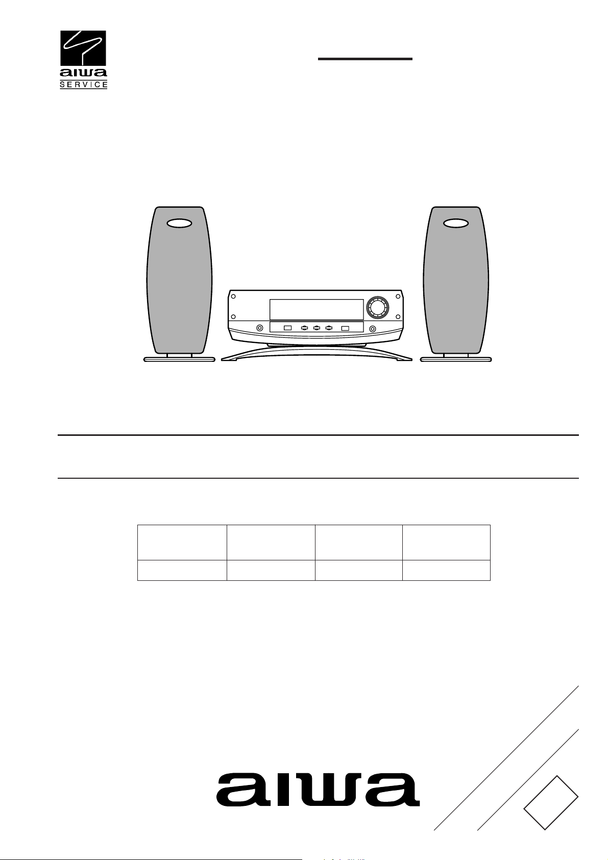
XR-X7
U, EZ, K, HR, C
SERVICE MANUAL
COMPACT DISC
STEREO SYSTEM
COMPACT
DISC
XR-X7
• This Service Manual is the “Revision Publishing” and replaces
“Simple Manual” of XR-X7 <U, EZ, K>, (S/M Code No. 09-015-445-8T1).
CX-LX7
BASIC CD MECHANISM : DA11B3
SPEAKERSYSTEM
SX-LX7
REMOTE
CONTROLLER
RC-BAT01(BS)
S/M Code No. 09-018-445-8R2
REVISION
DATA
Page 2

TABLE OF CONTENTS
SPECIFICATIONS ...............................................................................................................................................................3
PROTECTION OF EYES FROM LASER DURING SERVICING................................................................................... 4
ELECTRICAL MAIN PARTS LIST .............................................................................................................................. 5 ~ 9
TRANSISTOR ILLUSTRATION ........................................................................................................................................10
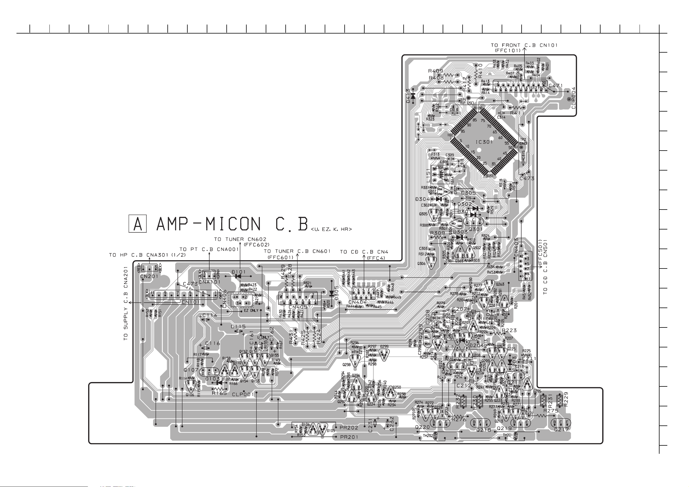
WIRING – 1 (AMP – MICON) <U, EZ, K, HR>.................................................................................................................. 11
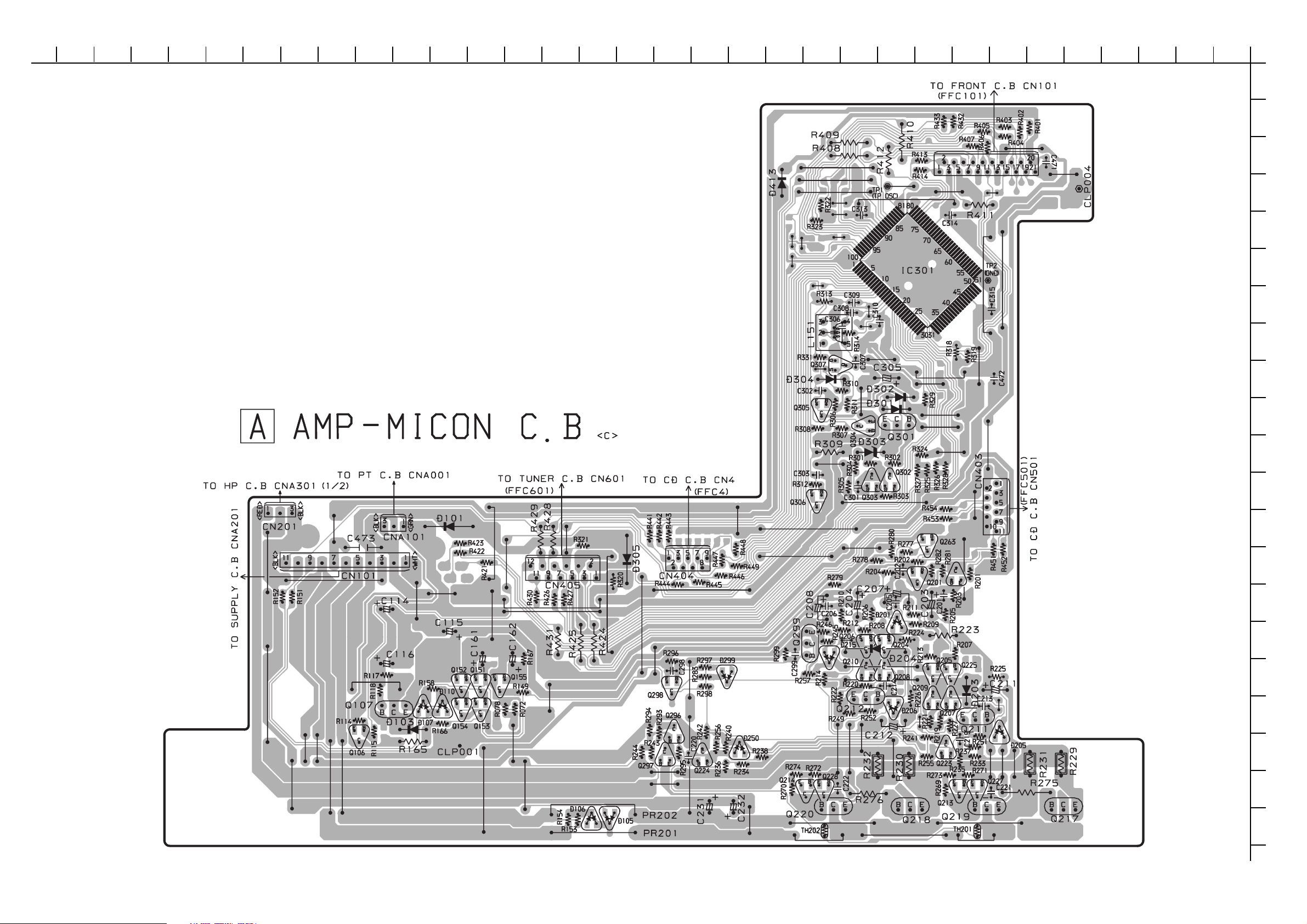
WIRING – 2 (AMP – MICON) <C>.................................................................................................................................... 12
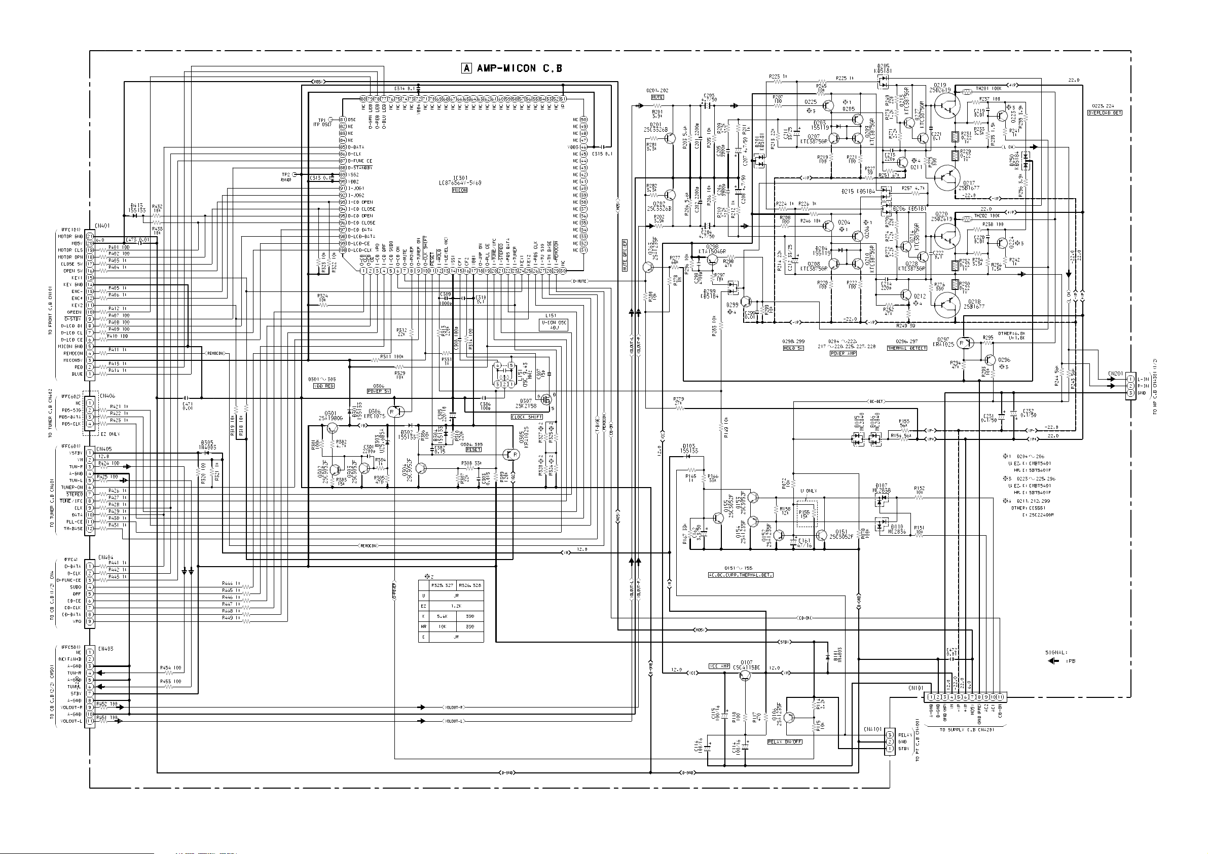
SCHEMATIC DIAGRAM – 1 (AMP – MICON) .................................................................................................................. 13
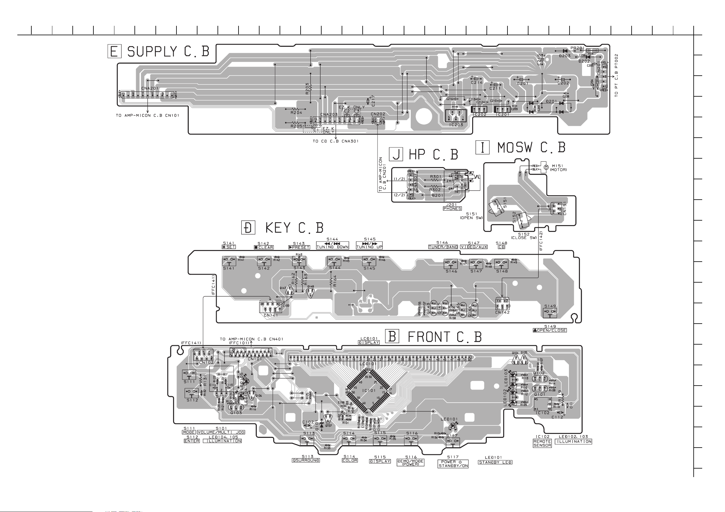
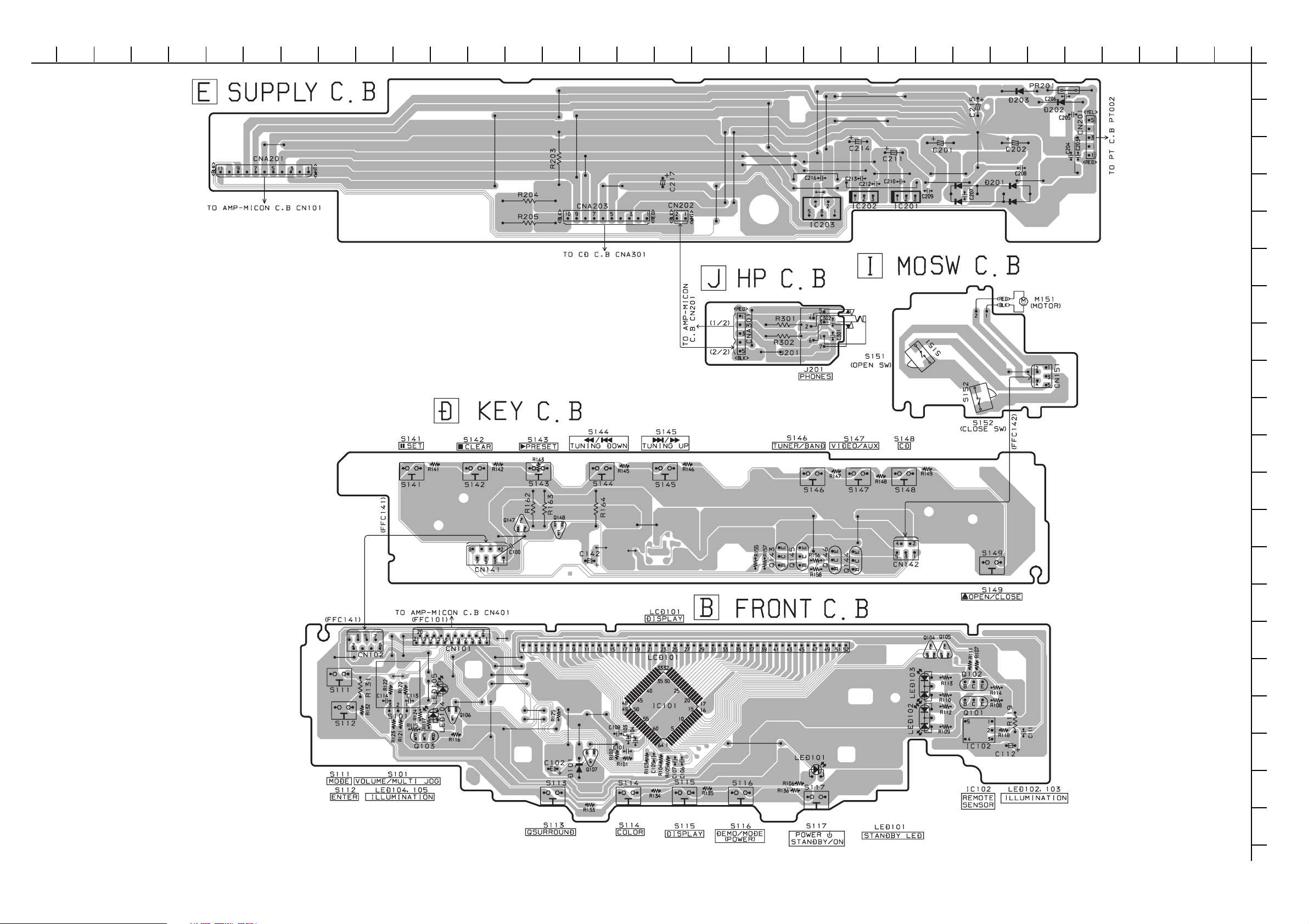
WIRING – 3 (FRONT / KEY / SUPPLY / MOSW / HP) <U, EZ, K> .................................................................................. 14
WIRING – 4 (FRONT / KEY / SUPPLY / MOSW / HP) <HR, C> ...................................................................................... 15
SCHEMATIC DIAGRAM – 2 (FRONT / KEY / MOSW)..................................................................................................... 16
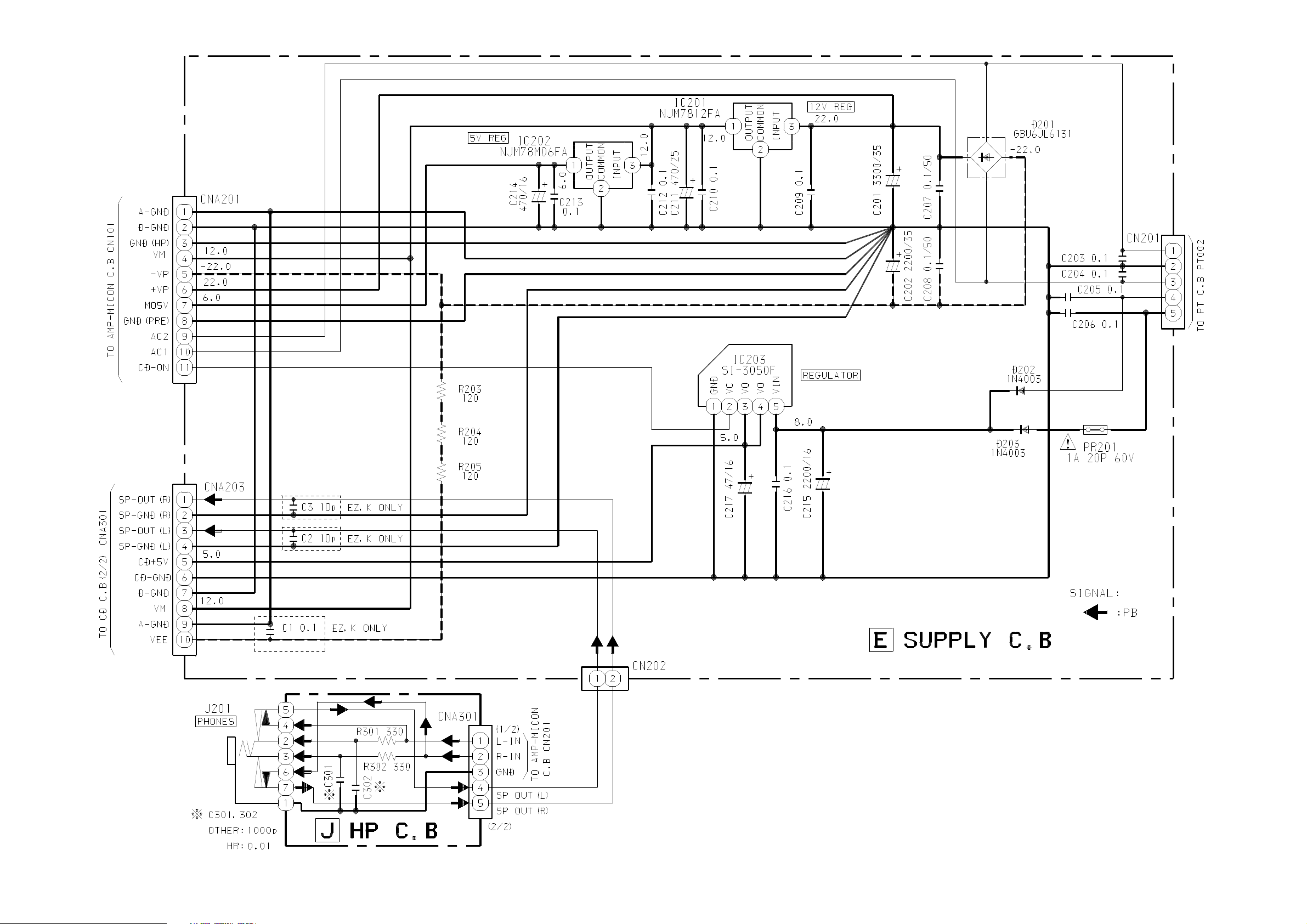
SCHEMATIC DIAGRAM – 3 (SUPPLY / HP).................................................................................................................... 17
WIRING – 5 (CD / JACK) <U, EZ, K> ...............................................................................................................................18
WIRING – 6 (CD / JACK) <HR, C> ................................................................................................................................... 19
WIRING – 7 (CD – MOTOR>.............................................................................................................................................20
SCHEMATIC DIAGRAM – 4 (CD 1 / 2 / CD – MOTOR) ................................................................................................... 21
SCHEMATIC DIAGRAM – 5 (CD 2 / 2 / JACK) ................................................................................................................ 22
WIRING – 8 (PT) <U, EZ, K, C> ....................................................................................................................................... 23
SCHEMATIC DIAGRAM – 6 (PT) <U, EZ, K, C>............................................................................................................. 24
WIRING – 9 (PT) <HR> .................................................................................................................................................... 25
SCHEMATIC DIAGRAM – 7 (PT) <HR>.......................................................................................................................... 26
WIRING – 10 (TUNER) <U, HR, C> ................................................................................................................................. 27
SCHEMATIC DIAGRAM – 8 (TUNER) <U, HR, C>......................................................................................................... 28
WIRING – 11 (TUNER) <EZ, K>....................................................................................................................................... 29
SCHEMATIC DIAGRAM – 9 (TUNER) <EZ, K> .............................................................................................................. 30
IC BLOCK DIAGRAM.................................................................................................................................................31, 32
LCD DIAGRAM .................................................................................................................................................................33
IC DESCRIPTION .....................................................................................................................................................34 ~ 39
ADJUSTMENT <TUNER / CD / AMP – MICON> ..................................................................................................... 40 ~ 44
CD TEST MODE .............................................................................................................................................................. 45
MECHANICAL PARTS ARRANGEMENT............................................................................................................... 46 ~ 51
MECHANICAL PARTS LIST 1 / 1 ................................................................................................................................... 52
CD MECHANISM EXPLODED VIEW 1 / 1 ....................................................................................................................53
CD MECHANISM PARTS LIST 1 / 1 ............................................................................................................................. 53
GENERAL SPEAKER DISASSEMBLY INSTRUCTIONS (FOR REFERENCE) .......................................................... 54
SPEAKER PARTS LIST <SX – LX7 (YJSN, YUJSN)>.................................................................................................. 55
ACCESSORIES / PACKAGE LIST ...................................................................................................................................55
– 2 –
Page 3

SPECIFICATIONS <EZ, K>
MAIN UNIT CX-LX7
TUNER
FM tuning range 87.5 MHz to 108 MHz
FM usable sensitivity (IHF) 16.8 dBf
FM antenna terminal 75 ohms (unbalanced)
MW tuning range 531 kHz to 1602 kHz (9 kHz step)
530 kHz to 1710 kHz (10 kHz step)
MW usable sensitivity 350 µV/m
LW tuning range 144 kHz to 290 kHz
LW usable sensitivity 1400 µV/m
MW/LW antenna Loop antenna
AMPLIFIER
Power output Rated: 16 W + 16 W
(6 ohms, THD 1 %, 1 kHz/DIN 45500)
Reference: 20 W + 20 W
(6 ohms, THD 10 %, 1 kHz/DIN 45324)
DIN MUSIC POWER: 30 W + 30 W
Input VIDEO/AUX: 400 mV
Outputs SPEAKERS: 6 ohms or more
PHONES: 16 ohms or more
SUB WOOFER: 1.0 V
DIGITAL OUT (OPTICAL) jack
LINE OUT jack
CD PLAYER
Laser Semiconductor laser (λ = 780 nm)
D/A converter 1 bit dual
Signal-to-noise ratio 85 dB (1 kHz, 0 dB)
Harmonic distortion 0.08 % (1 kHz, 0 dB)
Wow and flutter Unmeasurable
GENERAL
Power requirements 230 V AC, 50 Hz
Power consumption EZ: 50 W
K: 55 W
Power consumption in
standby mode EZ: With ECO mode on: 1.2 W
With ECO mode off: 13 W
K: With ECO mode on: 1.5 W
With ECO mode off: 15 W
Dimensions (W x H x D) 249 x 92 x 353 mm
Weight 3.5 kg
SPEAKER SYSTEM SX-LX7
Speaker system 2 way, bass reflex (magnetic shielded)
Speaker units Woofer: 80 mm cone
Tweeter: 25 mm dome
Impedance 6 ohms
Dimensions (W x H x D) 98 x 260 x 191 mm
Weight 1.6 kg
• Design and specifications are subject to change without notice.
SPECIFICATIONS <U, HR, C>
MAIN UNIT CX-LX7
TUNER
FM tuning range 87.5 MHz to 108 MHz
FM usable sensitivity (IHF) 13.2 dBf
FM antenna terminals 75 ohms (unbalanced)
AM tuning range 530 kHz to 1710 kHz (10 kHz step)
531 kHz to 1602 kHz (9 kHz step)
AM usable sensitivity 350 µV/m
AM antenna Loop antenna
AMPLIFIER
Power output <U, C> 16 W + 16 W
(150 Hz - 16 kHz, THD less than 1 %,
6 ohms)
20 W + 20 W
(1 kHz, THD less than 10 %, 6 ohms)
Total harmonic distortion <U, C>
0.1 % (6 W, 1 kHz, 6 ohms, DIN AUDIO)
Power output <HR> Rated: 16 W + 16 W
(6 ohms, THD 1 %, 1 kHz)
Reference: 20 W + 20 W
(6 ohms, THD 10 %, 1 kHz)
Input VIDEO/AUX: 400 mV
Outputs SPEAKERS: 6 ohms or more
PHONES: 16 ohms or more
SUB WOOFER: 1.0 V
DIGITAL OUT (OPTICAL) jack
LINE OUT jack
GENERAL
Power requirements U, C: 120 V AC, 60 Hz
HR: 120 / 220 - 240 V AC switchable
50 / 60 Hz
Power consumption U: 45 W
C: 50 W
HR: 60 W
Power consumption in
standby mode With ECO mode on: 1.0 W
U, C: With ECO mode off: 13 W
HR: With ECO mode off: 15 W
Dimensions (W x H x D) 249 x 92 x 350 mm
(9 7/8 x 3 3/4 x 13 7/8 in.)
Weight 3.5 kg (7 lbs 13 oz)
SPEAKER SYSTEM SX-LX7
Speaker system 2 way, bass reflex (magnetic shielded)
Speaker units Woofer: 80 mm (3 1/4 in.) cone
Tweeter: 25 mm (1 in.) dome
Impedance 6 ohms
Dimensions (W x H x D) 98 x 260 x 191 mm
(3 7/8 x 10 3/8 x 7 5/8 in.)
Weight 1.6 kg (3 lbs 10 oz)
• Design and specifications are subject to change without notice.
CD PLAYER
Laser Semiconductor laser (λ = 780 nm)
D/A converter 1 bit dual
Signal-to-noise ratio 85 dB (1 kHz, 0 dB)
Harmonic distortion 0.08 % (1 kHz, 0 dB)
Wow and flutter Unmeasurable
– 3 –
Page 4
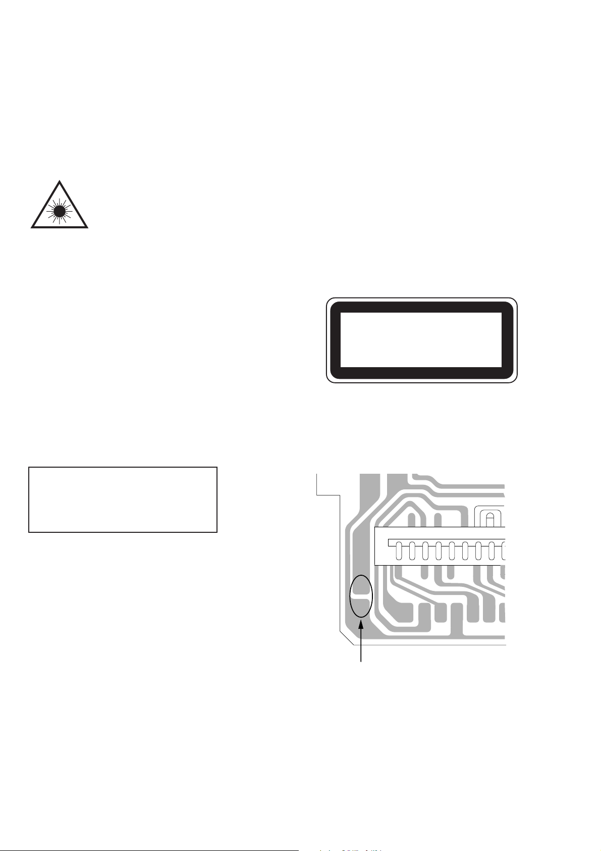
PROTECTION OF EYES FROM LASER BEAM DURING SERVICING
This set employs laser. Therefore, be sure to follow carefully
the instructions below when servicing.
WARNING!!
WHEN SERVICING, DO NOT APPROACH THE LASER
EXIT WITH THE EYE TOO CLOSELY. IN CASE IT IS
NECESSARY TO CONFIRM LASER BEAM EMISSION.
BE SURE TO OBSERVE FROM A DISTANCE OF MORE
THAN 30cm FROM THE SURFACE OF THE OBJECTIVE LENS ON THE OPTICAL PICK-UP BLOCK.
s Caution: Invisible laser radiation when
open and interlocks defeated avoid
exposure to beam.
s Advarsel: Usynlig laserståling ved åbning,
når sikkerhedsafbrydere er ude af funktion.
Undgå udsættelse for stråling.
VAROITUS!
Laiteen Käyttäminen muulla kuin tässä käyttöohjeessa
mainitulla tavalla saataa altistaa käyt-täjän
turvallisuusluokan 1 ylittävälle näkymättömälle
lasersäteilylle.
VARNING!
Om apparaten används på annat sätt än vad som
specificeras i denna bruksanvising, kan användaren
utsättas för osynling laserstrålning, som överskrider
gränsen för laserklass 1.
CAUTION
Use of controls or adjustments or performance of procedures other than those specified herin may result in
hazardous radiation exposure.
ATTENTION
L’utillisation de commandes, réglages ou procédures
autres que ceux spécifiés peut entraîner une dangereuse
exposition aux radiations.
ADVARSEL
Usynlig laserståling ved åbning, når sikkerhedsafbrydereer
ude af funktion. Undgå udsættelse for stråling.
This Compact Disc player is classified as a CLASS 1
LASER product.
The CLASS 1 LASER PRODUCT label is located on the
rear exterior.
CLASS 1 LASER PRODUCT
KLASSE 1 LASER PRODUKT
LUOKAN 1 LASER LAITE
KLASS 1 LASER APPARAT
Precaution to replace Optical block
(SF-P101NR)
Body or clothes electrostatic potential could
ruin laser diode in the optical block. Be sure
ground body and workbench, and use care the
clothes do not touch the diode.
1) After the connection, remove solder shown in
right figure.
PICK-UP Assy PWB
Solder
– 4 –
Page 5

ELECTRICAL MAIN PARTS LIST
PART NO. DESCRIPTIONREF. NO. KANRI
NO.
IC
87-A20-446-010 C-IC,LA9241ML
87-A21-319-010 C-IC,LC78622NE
87-017-917-080 IC,BU4066BCF
87-A21-968-030 C-IC,LC75824E
87-A22-043-010 IC,SPS-440-1-E1
87-A21-985-040 C-IC,BA5983FM
87-001-576-010 IC,MJM7812FA
87-002-349-010 IC,NJM78M06FA
87-A21-298-010 IC,SI-3050F
8B-CL2-601-030 C-IC,LC876564V-5V69
87-A21-452-130 C-IC,BD3876AKS2
87-A21-103-040 C-IC,MM1454XFBE
87-017-825-010 IC,GP1F32T
87-A21-928-010 IC,LC72131D-N
87-A20-440-040 C-IC,BU1920FS<EZ>
87-A20-913-010 IC,LA1837NL
TRANSISTOR
87-026-463-080 TR,2SA933SRS
87-026-245-080 TR,DTC114ES
87-A30-198-080 TR,KTC3199GR
87-026-609-080 TR,KTA1266GR
87-A30-427-040 C-TR,DTC114EKA
87-A30-075-080 C-TR,2SA1235F
87-A30-447-040 C-TR,DTA114EKA
87-A30-234-080 TR,CSC4115BC
87-A30-520-080 TR,2SC5342Y
87-A30-515-080 TR,2SA1979O/Y
87-A30-076-080 C-TR,2SC3052F
89-333-266-080 CHIP TR,2SC3326B
87-A30-107-070 C-TR,CMBT5401
87-A30-060-080 C-TR,KTC3875GR
87-A30-190-080 TR,CC5551
87-A30-306-010 TR,2SB1677
87-A30-307-010 TR,2SD2619
87-A30-257-080 C-TR,2SD1306E
87-A30-484-080 C-TR,KRA102S
87-A30-061-080 C-TR,KTA1504GR
87-A30-494-080 TR,2SA1980G
87-A30-490-080 C-TR,KRC107S
87-A30-087-080 C-FET,2SK2158
87-A30-287-040 C-TR,DTC114TKA
87-A30-196-080 TR,2SC4115SRS
89-327-143-080 C-TR,2SC2714O
87-A30-072-080 C-TR,RT1P 144C
87-A30-635-040 C-TR,SBT5401F<HR,C>
89-322-405-080 TR,2SC2240GR<C>
89-503-602-080 C-FET,2SK360E<EZ,K>
87-A30-086-070 C-TR,CSD1306E<EZ,K>
87-A30-074-080 C-TR,RT1P141C<EZ,K>
DIODE
87-020-465-080 DIODE,1SS133 (110MA)
87-070-274-080 DIODE,1N4003 SEM
87-070-136-080 ZENER,MTZJ5.1B
87-A40-313-080 C-DIODE,MC2840
87-A40-270-080 C-DIODE,MC2838
87-A40-269-080 C-DIODE,MC2836
87-A40-505-040 C-DIODE,KDS181
87-017-654-060 DIODE,GBU6JL6131
87-017-650-080 DIODE,1SS119
87-A40-504-040 C-DIODE,KDS184
87-A40-748-080 ZENER,UZ5.6BSA
87-A40-437-080 ZENER,MTZJ4.3B
87-017-148-080 ZENER,HZS6A1L
DESCRIPTIONREF. NO. KANRI
PART NO.
NO.
AMP-MICON C.B
C114 87-016-044-040 CAP,E 100-16 GAS
C115 87-016-044-040 CAP,E 100-16 GAS
C116 87-016-044-040 CAP,E 100-16 GAS
C161 87-010-553-040 CAP,E 47-16
C162 87-010-496-040 CAP,E 3.3-50 5L
C201 87-012-278-080 C-CAP,U 2200P-50 B
C202 87-012-278-080 C-CAP,U 2200P-50 B
C203 87-010-421-080 CAP, ELECT 4.7-50V
C204 87-A12-090-080 CAP,E 4.7-50 SMG
C205 87-012-281-080 C-CAP,U 3900P-50 B
C206 87-012-281-080 C-CAP,U 3900P-50 B
C207 87-A12-090-080 CAP,E 4.7-50 SMG
C208 87-A12-090-080 CAP,E 4.7-50 SMG
C211 87-A12-070-080 CAP,E 33-25 SMG
C212 87-A12-070-080 CAP,E 33-25 SMG
C213 87-012-266-080 C-CAP,U 220P-50 B
C214 87-012-266-080 C-CAP,U 220P-50 B
C219 87-012-286-080 C-CAP,U 0.01-25 K B
C220 87-012-286-080 C-CAP,U 0.01-25 K B
C221 87-010-831-080 C-CAP,U,0.1-16F
C222 87-010-831-080 C-CAP,U,0.1-16F
C231 87-010-490-040 CAP, ELECT 0.1-50
C232 87-010-490-040 CAP, ELECT 0.1-50
C298 87-012-282-080 C-CAP,U 4700P-50 K B
C299 87-012-286-080 C-CAP,U 0.01-25 K B
C301 87-012-278-080 C-CAP,U 2200P-50 B
C302 87-A10-781-080 C-CAP,U 0.15-10 K B
C303 87-010-785-080 C-CAP,U0.015-25BK
C305 87-A12-063-080 CAP,E 220-10 SMG
C306 87-012-195-080 C-CAP,U 100P-50CH
C307 87-012-176-080 C-CAP,U 15P-50 J CH
C308 87-012-198-080 C-CAP,U 180P-50 J CH
C309 87-012-274-080 CHIP CAP,U 1000P-50B
C310 87-010-831-080 C-CAP,U,0.1-16F
C313 87-010-831-080 C-CAP,U,0.1-16F
C314 87-010-831-080 C-CAP,U,0.1-16F
C315 87-010-831-080 C-CAP,U,0.1-16F
C471 87-A11-132-080 CAP,TC U 0.01-50 K B<EXCEPT C>
C471 87-012-286-080 C-CAP,U 0.01-25 KB<C>
C472 87-A11-132-080 CAP,TC U 0.01-50 K B<EXCEPT C>
C472 87-012-286-080 C-CAP,U 0.01-25 KB<C>
C473 87-A11-132-080 CAP,TC U 0.01-50 K B
CN101 87-099-411-010 CONN,11P V WHT EH
CN201 87-049-919-010 CONN,3P V WHT EH
CN401 87-A61-370-010 CONN,21P V BLK FMN-BTRK
CN403 87-A61-272-010 CONN,11P V BLK FMN-BTRK
CN404 87-A60-900-010 CONN,9P V BLK FMN-BTRK
CN405 87-099-014-010 CONN,12P V BLK 6216
CN406 87-099-211-010 CONN,4P V BLK 6216<EZ>
CNA101 87-A60-620-010 CONN,3P V 2MM JMT
L151 87-A50-333-010 COIL,OSC 9.43MHZ
R229 87-A00-258-080 RES,M/F 0.22-1W J
R230 87-A00-258-080 RES,M/F 0.22-1W J
R231 87-A00-258-080 RES,M/F 0.22-1W J
R232 87-A00-258-080 RES,M/F 0.22-1W J
R319 87-022-239-080 C-RES U 10K-1/16WF
R324 87-022-239-080 C-RES U 10K-1/16WF
TH201 87-A91-042-080 C-THMS,100K 55001
TH202 87-A91-042-080 C-THMS,100K 55001
FRONT C.B
C101 87-012-195-080 C-CAP,U 100P-50CH
C102 87-010-560-040 CAP,E 10-50 GAS
C103 87-010-829-080 CAP, U 0.047-16
C104 87-010-829-080 CAP, U 0.047-16
C105 87-012-195-080 C-CAP,U 100P-50CH
C106 87-012-195-080 C-CAP,U 100P-50CH
– 5 –
Page 6

PART NO. DESCRIPTIONREF. NO. KANRI
NO.
C107 87-012-195-080 C-CAP,U 100P-50CH
C108 87-010-831-080 C-CAP,U,0.1-16F
C111 87-012-274-080 CHIP CAP,U 1000P-50B
C112 87-010-560-040 CAP,E 10-50 GAS
C113 87-012-286-080 C-CAP,U 0.01-25 K B
C114 87-012-286-080 C-CAP,U 0.01-25 K B
CN101 87-A61-370-010 CONN,21P V BLK FMN-BTRK
CN102 87-099-201-010 CONN,8P H BLK 6216
FFC101 8B-CL2-660-010 FF-CABLE,21P 1.0
LCD101 8B-CL2-605-010 LCD,AIW4277-30PIN BCL-2
LED101 87-A40-317-080 LED,SLR-342VCT31 RED
LED102 87-A92-077-010 LED,SMLU1BE16C-SLF73 BLU/UMB
LED103 87-A92-077-010 LED,SMLU1BE16C-SLF73 BLU/UMB
LED104 87-A41-054-010 LED,SELV1D10CXM-S GREEN<U,EZ,K>
LED104 87-A92-078-010 LED,SELU1D10CXM-SLF38 GR<HR,C>
LED105 87-A41-054-010 LED,SELV1D10CXM-S GREEN<U,EZ,K>
LED105 87-A92-078-010 LED,SELU1D10CXM-SLF38 GR<HR,C>
S101 87-A91-633-010 SW,RTRY XRE012103PVB25FINA 1-2
S111 87-A90-095-080 SW,TACT EVQ11G04M
S112 87-A90-095-080 SW,TACT EVQ11G04M
S113 87-A90-095-080 SW,TACT EVQ11G04M
S114 87-A90-095-080 SW,TACT EVQ11G04M
S115 87-A90-095-080 SW,TACT EVQ11G04M
S116 87-A90-095-080 SW,TACT EVQ11G04M
S117 87-A90-095-080 SW,TACT EVQ11G04M
CD C.B
C1 87-010-418-040 CAP,E 3.3-25 5L
C2 87-012-286-080 C-CAP,U 0.01-25 K B
C3 87-010-263-040 CAP,E 100-10
C4 87-A12-063-040 CAP,E 220-10 SMG
C5 87-012-286-080 C-CAP,U 0.01-25 K B
C6 87-010-234-040 CAP,E 47-16 5L
C7 87-012-274-080 CHIP CAP,U 1000P-50B
C8 87-010-787-080 C-CAP,U 0.022-25 K B
C9 87-A12-063-040 CAP,E 220-10 SMG
C10 87-010-263-040 CAP,E 100-10 M 11L SME
C11 87-A10-794-080 C-CAP,U 0.15-16 Z F
C12 87-010-071-040 CAP,E 1-50 M 5L SRE
C13 87-010-788-080 C-CAP,U 0.033-25 Z F
C14 87-010-405-040 CAP,E 10-50 M 11L SME
C16 87-015-962-040 CAP,E 0.22-50 M 5L SRE
C17 87-012-268-080 C-CAP,U 330P-50 B
C18 87-010-785-080 C-CAP,U0.015-25BK
C19 87-A10-706-080 C-CAP,U 0.33-16 Z F
C20 87-010-788-080 C-CAP,U 0.033-25 Z F
C21 87-A10-794-080 C-CAP,U 0.15-16 Z F
C22 87-012-280-080 C-CAP,U 3300P-50 K B
C23 87-A10-504-080 C-CAP,U 0.047-16 K B
C24 87-A10-025-080 C-CAP,U 0.22-16Z F
C25 87-012-272-080 C-CAP,U 680P-50 B
C26 87-A10-706-080 C-CAP,U 0.33-16 Z F
C28 87-012-286-080 C-CAP,U 0.01-25 K B
C29 87-012-282-080 C-CAP,U 4700P-50 K B
C30 87-012-199-080 C-CAP,U 220P-50 J CH
C31 87-010-068-040 CAP E 0.22-50 5L
C32 87-015-680-040 CAP,E 47-10 7L
C33 87-010-071-040 CAP,E 1-50 M 5L SRE
C34 87-012-280-080 C-CAP,U 3300P-50 K B
C35 87-012-286-080 C-CAP,U 0.01-25 K B
C36 87-010-374-040 CAP,E 47-10
C37 87-010-404-040 CAP,E 4.7-50 SME
C38 87-010-831-080 C-CAP,U,0.1-16F
C39 87-012-274-080 CHIP CAP,U 1000P-50B
C40 87-012-162-080 C-CAP,U 1P-50 CK
C41 87-012-280-080 C-CAP,U 3300P-50 K B
C42 87-012-176-080 C-CAP,U 15P-50 J CH
C45 87-010-831-080 C-CAP,U,0.1-16F
C46 87-010-831-080 C-CAP,U,0.1-16F
DESCRIPTIONREF. NO. KANRI
PART NO.
NO.
C47 87-010-831-080 C-CAP,U,0.1-16F<U,EZ,K,C>
C48 87-012-182-080 C-CAP,U 27P-50 CH
C51 87-012-199-080 C-CAP,U 220P-50 J CH
C53 87-012-195-080 C-CAP,U 100P-50CH
C55 87-010-263-040 CAP,E 100-10<U,EZ,K,C>
C57 87-012-184-080 C-CAP,U 33P-50 CH
C58 87-012-184-080 C-CAP,U 33P-50 CH
C59 87-010-263-040 CAP,E 100-10
C60 87-010-831-080 C-CAP,U,0.1-16F<U,EZ,K,C>
C61 87-010-831-080 C-CAP,U,0.1-16F<U,EZ,K,C>
C62 87-A12-058-040 CAP,E 470-6.3 SMG
C65 87-010-404-040 CAP,E 4.7-50 SME
C66 87-010-831-080 C-CAP,U,0.1-16F<U,EZ,K,C>
C67 87-010-263-040 CAP,E 100-10<U,EZ,K,C>
C69 87-012-197-080 C-CAP,U 150P-50 CH
C70 87-018-134-080 CAP,TC U 0.01-16 NY UP050<C>
C71 87-018-208-080 CAP,TC U 0.047-50 ZF<C>
C72 87-012-286-080 C-CAP,U 0.01-25 K B<C>
C73 87-010-831-080 C-CAP,U 0.1-16 ZF<C>
C74 87-018-208-080 CAP,TC U 0.047-50 ZF<C>
C75 87-010-831-080 C-CAP,U 0.1-16 ZF<C>
C76 87-010-831-080 C-CAP,U 0.1-16 ZF<C>
C81 87-010-417-040 CAP,E 2.2-35 5L
C82 87-010-417-040 CAP,E 2.2-35 5L
C83 87-012-277-080 C-CAP, U 1800P-50 B
C84 87-012-277-080 C-CAP, U 1800P-50 B
C93 87-A10-260-080 C-CAP,U 0.1-16 K B<U,EZ,K,C>
C94 87-A10-260-080 C-CAP,U 0.1-16 K B<U,EZ,K,C>
C95 87-012-286-080 C-CAP,U 0.01-25 K B
C100 87-018-131-080 CAP,TC U 1000P-50<EZ,K>
C101 87-012-195-080 C-CAP,U 100P-50CH
C102 87-012-195-080 C-CAP,U 100P-50CH
C103 87-012-195-080 C-CAP,U 100P-50CH
C104 87-012-195-080 C-CAP,U 100P-50CH
C105 87-012-195-080 C-CAP,U 100P-50CH
C106 87-010-494-040 CAP,E 1-50 GAS
C110 87-010-831-080 C-CAP,U,0.1-16F
C120 87-A12-326-080 CAP,E 1000-16 RS
C121 87-012-286-080 C-CAP,U 0.01-25 K B
C123 87-012-286-080 C-CAP,U 0.01-25 K B
C124 87-012-199-080 C-CAP,U 220P-50 K B
C125 87-012-270-080 C-CAP,U 470P-50 K B
C126 87-012-270-080 C-CAP,U 470P-50 K B
C127 87-012-199-080 C-CAP,U 220P-50 J CH
C200 87-018-131-080 CAP,TC U 1000P-50<EZ,K>
C201 87-012-199-080 C-CAP,U 220P-50 J CH
C202 87-012-199-080 C-CAP,U 220P-50 J CH
C213 87-010-758-080 C-CAP,U 0.068-25F
C214 87-010-758-080 C-CAP,U 0.068-25F
C215 87-010-544-040 CAP,E 0.1-50 SME
C216 87-010-544-040 CAP,E 0.1-50 SME
C217 87-012-278-080 C-CAP,U 2200P-50 B
C218 87-012-278-080 C-CAP,U 2200P-50 B
C301 87-010-235-080 CAP,E 470-16 SME
C302 87-010-112-040 CAP,E 100-16
C303 87-010-553-040 CAP,E 47-16 GAS
C304 87-010-404-040 CAP,E 4.7-50 SME
C305 87-010-494-040 CAP,E 1-50 GAS
C495 87-010-831-080 C-CAP,U,0.1-16F
C496 87-012-286-080 C-CAP,U 0.01-25 K B
C501 87-A12-071-040 CAP,E 47-25 SMG
C502 87-A12-071-040 CAP,E 47-25 SMG
C503 87-012-274-080 CHIP CAP,U 1000P-50B
C504 87-012-274-080 CHIP CAP,U 1000P-50B
C511 87-012-276-080 C-CAP,U 1500P-50 K B
C512 87-012-276-080 C-CAP,U 1500P-50 K B
C521 87-010-758-080 C-CAP,U 0.068-25F
C522 87-A11-070-080 C-CAP,U 0.033-16 K B
C524 87-010-401-040 CAP,E 1-50 SME
C525 87-A10-260-080 C-CAP,U 0.1-16 K B
– 6 –
Page 7

PART NO. DESCRIPTIONREF. NO. KANRI
DESCRIPTIONREF. NO. KANRI
NO.
C526 87-A10-260-080 C-CAP,U 0.1-16 K B
C527 87-012-286-080 C-CAP,U 0.01-25 K B
C528 87-012-286-080 C-CAP,U 0.01-25 K B
C531 87-010-421-040 CAP,E 4.7-50 5L
C532 87-010-421-040 CAP,E 4.7-50 5L
C535 87-A10-504-080 C-CAP,U 0.047-16 K B
C536 87-A10-504-080 C-CAP,U 0.047-16 K B
C537 87-010-493-040 CAP,E 0.47-50 M 5L SRE
C538 87-010-493-040 CAP,E 0.47-50 M 5L SRE
C539 87-012-281-080 C-CAP,U 3900P-50 B
C540 87-012-281-080 C-CAP,U 3900P-50 B
C541 87-A10-260-080 C-CAP,U 0.1-16 K B
C542 87-A10-260-080 C-CAP,U 0.1-16 K B
C543 87-A10-260-080 C-CAP,U 0.1-16 K B
C544 87-A10-260-080 C-CAP,U 0.1-16 K B
C545 87-A10-260-080 C-CAP,U 0.1-16 K B
C546 87-010-403-040 CAP,E 3.3-50 M 11L SME
C547 87-010-401-040 CAP,E 1-50 SME
C549 87-010-071-040 CAP,E 1-50 M 5L SRE
C550 87-010-071-040 CAP,E 1-50 M 5L SRE
C595 87-012-286-080 C-CAP,U 0.01-25 KB<HR>
C603 87-010-402-040 CAP,E 2.2-50 SME
C604 87-010-402-040 CAP,E 2.2-50 SME
C605 87-010-408-040 CAP,E 47-50 SME
C607 87-010-405-040 CAP,E 10-50
C608 87-010-405-040 CAP,E 10-50
C609 87-010-759-080 C-CAP,U, 0.1-25F
C610 87-010-384-040 CAP,E 100-25 SME
C611 87-012-286-080 C-CAP,U 0.01-25 K B
C612 87-012-286-080 C-CAP,U 0.01-25 K B
C702 87-010-374-040 CAP,E 47-10
C703 87-010-831-080 C-CAP,U,0.1-16F
C913 87-012-286-080 C-CAP,U 0.01-25 K B
CN1 87-A60-429-010 CONN,16P H TOC-A
CN2 87-A60-623-010 CONN,6P V 2MM JMT
CN4 87-A60-900-010 CONN,9P V BLK FMN-BTRK
CN201 87-A60-059-010 CONN,08P V 9604S-08C
CN302 87-A60-619-010 CONN,2P V 2MM JMT
CN501 87-A61-272-010 CONN,11P V BLK FMN-BTRK
CNA301 87-099-410-010 CONN,10P V WHT EH
CON2 86-ZG1-609-010 CONN ASSY,6P
FFC1 8B-CL2-663-010 FF-CABLE,16P 1.0
FFC4 8B-CL2-661-010 FF-CABLE,9P 1.0
FFC501 8B-CL2-662-010 FF-CABLE,11P 1.0
!
J202 87-YP6-608-010 TERMINAL,SPKR 4P
JR58 87-A50-189-080 C-COIL,S BLM21B272S
JR101 87-A50-189-080 C-COIL,S BLM21B272S
!
!
JW38 87-008-372-080 FLTR,EMI BL01 RN1
JW39 87-008-372-010 FLTR,EMIBL01 RN1<EZ,K>
JW43 87-008-372-010 FLTR,EMIBL01 RN1<HR>
L1 87-003-102-080 COIL,10UH J LAL02
L2 87-003-146-080 COIL,15UH J LAL02
!
!
!
L3 87-008-372-080 FLTR,EMI BL01 RN1
L4 87-003-102-080 COIL,10UH J LAL02
L5 87-003-152-080 COIL,100UH J LAL02
L6 87-003-102-080 COIL,10UH J LAL02
L7 87-003-102-080 COIL,10UH J LAL02
L8 87-003-102-080 COIL,10UH J LAL02
L201 87-003-383-010 COIL,1UH K
L202 87-003-383-010 COIL,1UH K
SFR130 87-024-437-080 SFR,100K H RH063MC
X1 87-A70-046-010 VIB,XTAL 16.934MHZ
KEY C.B
!
!
!
!
!
!
!
!
!
!
!
!
!
C100 87-018-131-080 CAP,TC U 1000P-50K
C142 87-010-553-040 CAP,E 47-16 M 5L SRE<HR,C>
CN141 87-A60-156-010 CONN,08P H FE<U>
CN141 87-A60-079-010 CONN,08P H 9604S-08F<EZ,K,HR,C>
CN142 87-A60-153-010 CONN,05P H FE<U>
PART NO.
NO.
CN142 87-A60-082-010 CONN,05P H 9604S-05F<EZ,K,HR,C>
FFC141 88-908-201-110 FF-CABLE,8P 1.25
FFC142 88-905-121-110 FF-CABLE, 5P 120MM
S141 87-A90-095-080 SW,TACT EVQ11G04M
S142 87-A90-095-080 SW,TACT EVQ11G04M
S143 87-A90-095-080 SW,TACT EVQ11G04M
S144 87-A90-095-080 SW,TACT EVQ11G04M
S145 87-A90-095-080 SW,TACT EVQ11G04M
S146 87-A90-095-080 SW,TACT EVQ11G04M
S147 87-A90-095-080 SW,TACT EVQ11G04M
S148 87-A90-095-080 SW,TACT EVQ11G04M
S149 87-A90-095-080 SW,TACT EVQ11G04M
SUPPLY C.B
C1 87-A11-148-080 CAP,TC U 0.1-50Z<EZ,K>
C2 87-018-104-080 CAP,TC U 10P-50<EZ,K>
C3 87-018-104-080 CAP,TC U 10P-50<EZ,K>
C201 87-A10-520-000 CAP,E 3300-35 M SMG
C202 87-016-051-000 CAP,E 2200-35 M SMG
C203 87-A12-317-080 C-CAP,U 0.1-50 Z F
C204 87-A12-317-080 C-CAP,U 0.1-50 Z F
C205 87-010-831-080 C-CAP,U,0.1-16F
C206 87-010-831-080 C-CAP,U,0.1-16F
C207 87-A12-317-080 C-CAP,U 0.1-50 Z F
C208 87-A12-317-080 C-CAP,U 0.1-50 Z F
C209 87-010-831-080 C-CAP,U,0.1-16F
C210 87-010-831-080 C-CAP,U,0.1-16F
C211 87-A12-074-080 CAP,E 470-25 SMG
C212 87-010-831-080 C-CAP,U,0.1-16F
C213 87-010-831-080 C-CAP,U,0.1-16F
C214 87-A12-068-080 CAP,E 470-16 SMG
C215 87-016-521-010 CAP,E2200-16 SMG
C216 87-010-831-080 C-CAP,U,0.1-16F
C217 87-010-380-040 CAP,E 47-16 M 11L SMG
CN201 87-009-195-010 CONN,5P V WHT EH
CN202 87-099-043-010 CONN 2P V WHT EH
CNA201 8B-CL2-671-010 CONN ASSY,11P EH
CNA203 8B-CL2-668-010 CONN ASSY,10P EH
PR201 87-A91-935-080 PROTECTOR,1A 20P 60V
PT C.B
C1 87-A10-479-080 CAP,CER 2200P-250 M E KH<EXCEPT HR>
C14 87-A10-831-080 CAP,E 1000-25 M SMG
C16 87-010-496-080 CAP,E 3.3-50 5L
CN1 87-A60-645-010 CONN,3P V VH<U,EZ,K,C>
CN1 87-A60-851-010 CONN,9P V VH<HR>
CNA1 8B-CL2-669-010 CONN ASSY,3P V STBY
CNA2 88-805-021-090 CONN ASSY,2P<HR>
CNA3 8B-CL2-673-010 CONN ASSY,7P V RY<HR>
F1 87-A91-224-010 FUSE,1.25A 125V<U>
FC1 87-033-213-080 FUSE CLAMP,PFC5000<U>
FC2 87-033-213-080 FUSE CLAMP,PFC5000<U>
PT1 8A-NF8-661-010 PT,SUB ANF-8 (U)<U,C>
PT1 8A-NF8-662-010 PT,SUB ANF-8 (E)<EZ,K>
PT1 8A-NF8-663-010 PT,SUB ANF-8 (H)<HR>
PT2 8B-CL2-650-010 PT,BCL-2 U<U>
PT2 8B-CL2-652-010 PT,BCL-2 EZ<EZ,K>
PT2 8B-CL2-653-010 PT,BCL-2 HR<HR>
PT2 8B-CL2-654-010 PT,BCL-2 C<C>
R3 87-A01-010-080 RES,SD 2.2M-1/2W J RCR50+<C>
RY1 87-A90-977-010 RELAY,AC12V DG12D1-O(M)<U,EZ,K,C>
S1 87-A90-234-010 SW,SL 1-2-2 SWS2201<HR>
T1 87-A60-317-010 TERMINAL, 1P MSC
T2 87-A60-317-010 TERMINAL, 1P MSC
TUNER C.B
C701 87-A12-071-080 CAP,E 47-25 SMG
– 7 –
Page 8

PART NO. DESCRIPTIONREF. NO. KANRI
NO.
C702 87-A12-090-080 CAP,E 4.7-50 SMG
C703 87-012-286-080 C-CAP,U 0.01-25 K B
C704 87-012-286-080 C-CAP,U 0.01-25 K B
C709 87-012-195-080 C-CAP,U 100P-50CH
C711 87-A12-062-080 CAP,E 100-10 SMG
C712 87-010-196-080 CHIP CAPACITOR,0.1-25
C713 87-012-286-080 C-CAP,U 0.01-25 K B
C714 87-012-286-080 C-CAP,U 0.01-25 K B
C715 87-012-195-080 C-CAP,U 100P-50 J CH<EZ,K>
C717 87-012-286-080 C-CAP,U 0.01-25 K B
C719 87-012-286-080 C-CAP,U 0.01-25 K B
C720 87-012-195-080 C-CAP,U 100P-50 J CH<EZ,K>
C721 87-012-176-080 C-CAP,U 15P-50 J CH
C722 87-012-176-080 C-CAP,U 15P-50 J CH
C723 87-012-274-080 CHIP CAP,U 1000P-50B
C725 87-012-274-080 CHIP CAP,U 1000P-50B
C727 87-010-196-080 CHIP CAPACITOR,0.1-25
C728 87-A12-063-080 CAP,E 220-10 SMG
C753 87-012-195-080 C-CAP,U 100P-50 J CH<EZ,K>
C755 87-012-286-080 C-CAP,U 0.01-25 K B
C756 87-012-286-080 C-CAP,U 0.01-25 K B
C757 87-012-188-080 C-CAP,U 47P-50 CH
C758 87-012-167-080 C-CAP,U 5P-50 CH
C761 87-010-196-080 CHIP CAPACITOR,0.1-25
C762 87-012-286-080 C-CAP,U 0.01-25 K B<EZ,K>
C763 87-010-829-080 C-CAP,U 0.047-16 Z F
C764 87-012-337-080 C-CAP,U 56P-50 CH<U,HR,C>
C765 87-012-286-080 C-CAP,U 0.01-25 K B
C766 87-012-286-080 C-CAP,U 0.01-25 K B
C768 87-012-286-080 C-CAP,U 0.01-25 K B<EZ,K>
C769 87-A12-071-080 CAP,E 47-25 SMG
C770 87-010-829-080 C-CAP,U 0.047-16 Z F
C771 87-A12-070-080 CAP,E 33-25 SMG
C772 87-010-829-080 C-CAP,U 0.047-16 Z F
C773 87-010-196-080 CHIP CAPACITOR,0.1-25<U,HR,C>
C773 87-015-785-080 CHIP CAPACITOR,0.1-25<EZ,K>
C774 87-A12-062-080 CAP,E 100-10 SMG
C775 87-A12-090-080 CAP,E 4.7-50 SMG
C776 87-012-286-080 C-CAP,U 0.01-25 K B
C777 87-A12-086-080 CAP,E 0.47-50 SMG
C778 87-A12-087-080 CAP,E 1-50 SMG
C779 87-A12-087-080 CAP,E 1-50 SMG
C780 87-010-196-080 CHIP CAPACITOR,0.1-25
C781 87-A12-091-080 CAP,E 10-50 SMG
C782 87-A12-091-080 CAP,E 10-50 SMG
C783 87-012-286-080 C-CAP,U 0.01-25 K B
C784 87-012-286-080 C-CAP,U 0.01-25 K B
C785 87-010-805-080 C-CAP,S 1-16 Z F
C786 87-010-805-080 C-CAP,S 1-16 Z F
C787 87-012-280-080 C-CAP,U 3300P-50 K B
C788 87-012-280-080 C-CAP,U 3300P-50 K B
C789 87-012-275-080 C-CAP,U 1200P-50 B
C790 87-012-275-080 C-CAP,U 1200P-50 B
C791 87-A12-091-080 CAP,E 10-50 SMG
C793 87-012-273-080 C-CAP,U 820P-50 B<U,HR,C>
C793 87-012-274-080 C-CAP,U 1000P-50 KB<EZ,K>
C794 87-A12-092-080 CAP,E 22-50 SMG
C795 87-010-829-080 C-CAP,U 0.047-16 ZF<EZ,K>
C795 87-010-596-080 C-CAP,U 0.047-16 KR<U,HR,C>
C796 87-A12-089-080 CAP,E 3.3-50 SMG
C797 87-012-276-080 C-CAP,U 1500P-50 K B<EZ,K,HR>
C797 87-012-278-080 C-CAP,U 2200P-50 K B<U,C>
C798 87-012-276-080 C-CAP,U 1500P-50 K B<EZ,K,HR>
C798 87-012-278-080 C-CAP,U 2200P-50 K B<U,C>
C799 87-010-829-080 C-CAP,U 0.047-16 Z F
C812 87-012-286-080 C-CAP,U 0.01-25 K B
C813 87-010-197-080 CAP, CHIP 0.01 DM<U,HR,C>
C814 87-012-286-080 C-CAP,U 0.01-25 K B
C819 87-010-197-080 CAP, CHIP 0.01 DM<U,HR,C>
C820 87-A12-071-080 CAP,E 47-25 SMG
DESCRIPTIONREF. NO. KANRI
PART NO.
NO.
C821 87-012-286-080 C-CAP,U 0.01-25 K B
C822 87-012-286-080 C-CAP,U 0.01-25 K B
C823 87-012-286-080 C-CAP,U 0.01-25 K B
C828 87-010-196-080 CHIP CAPACITOR,0.1-25
C829 87-010-196-080 CHIP CAPACITOR,0.1-25
C859 87-012-286-080 C-CAP,U 0.01-25 K B<EZ>
C861 87-012-199-080 C-CAP,U 220P-50 J CH<EZ>
C862 87-012-199-080 C-CAP,U 220P-50 J CH<EZ>
C863 87-012-270-080 C-CAP,U 470P-50 KB<EZ>
C864 87-A12-091-080 CAP,E 10-50 SMG<EZ>
C865 87-010-196-080 CHIP CAPACITOR,0.1-25<EZ>
C866 87-A12-091-080 CAP,E 10-50 SMG<EZ>
C867 87-012-286-080 C-CAP,U 0.01-25 K B<EZ>
C868 87-012-184-080 C-CAP,U 33P-50 J CH<EZ>
C869 87-012-180-080 C-CAP,U 22P-50 J CH<EZ>
C940 87-012-286-080 C-CAP,U 0.01-25 K B<EZ,K>
C942 87-012-172-080 C-CAP,U 10P-50 D CH<EZ,K>
C947 87-012-286-080 C-CAP,U 0.01-25 K B<EZ,K>
C949 87-A10-039-080 C-CAP,U 470P-50 J CH<EZ,K>
C952 87-012-286-080 C-CAP,U 0.01-25 K B<EZ,K>
C958 87-012-286-080 C-CAP,U 0.01-25 K B<EZ,K>
C959 87-010-196-080 CHIP CAPACITOR,0.1-25
C960 87-010-196-080 CHIP CAPACITOR,0.1-25
C961 87-012-170-080 C-CAP,U 8P-50 CH<U,HR,C>
C962 87-A12-087-080 CAP,E 1-50 SMG<EZ,K>
CF801 87-008-261-010 FLTR,CF SFE10.7MA5<U,HR,C>
CF801 87-008-423-010 FLTR,CF SFE10.7MS3G-A<EZ,K>
CF802 87-008-261-010 FLTR,CF SFE10.7MA5<U,HR,C>
CF802 82-785-747-010 CF,MS2 GHY,R<EZ,K>
CN601 87-099-029-010 CONN,12P H BLK 6216
CN602 87-099-211-010 CONN,4P V BLK 6216<EZ>
FFC601 88-912-081-110 FF-CABLE,12P 1.25 80MM
FFC602 88-904-081-110 FF-CABLE,4P 1.25 80MM<EZ>
FFE801 A8-6ZA-19H-030 6ZA-1 FEMENM<EZ,K>
FFE801 A8-8ZA-194-030 8ZA-1 FEMUNM<U,HR,C>
J801 87-A60-657-010 TERMINAL,4P HSP-154V5-02<U,HR,C>
J802 87-033-241-010 TERMINAL,ANT 2P AJ-2040<EZ,K>
L771 87-A50-266-010 COIL,FM DET-2N(TOK)
L772 87-A90-733-010 FLTR,PCFAZH-450(TOK)
L781 87-005-847-080 COIL,2.2UH K CECS
L791 87-A50-027-010 COIL,1 POLE MPX(TOK)<EZ,K)
L792 87-A50-027-010 COIL,1 POLE MPX(TOK)<EZ,K)
L832 87-005-847-080 COIL,2.2UH K CECS
L941 87-A50-020-010 COIL,ANT LW(COI)252KHZ<EZ,K>
L942 87-A50-019-010 COIL,OSC LW(COI)856KHZ<EZ,K>
L981 87-NF4-650-010 COIL,AM PACK4N(TOK)<U,HR,C>
L981 87-NF4-651-110 COIL,AM PACK2N(TOM)<EZ,K>
TC942 87-011-164-010 TRIMMER,CER 30P 4.5X3.9 VCT31<EZ,K>
X721 87-A70-306-010 VIB,XTAL4.5MHZ CSA-309ST<EZ,K,HR,C>
X721 87-A70-061-010 VIB,XTAL 4.500MHZ CSA-309<U>
X750 87-030-394-010 VIB,CER 3.5498MHZ CSA MGF228<EZ,K>
X851 87-A70-091-010 VIB,XTAL 4.332MHz CSA-309<EZ>
JACK C.B
CN202 87-A60-059-010 CONN,08P V 9604S-08C
FFC202 88-908-121-110 FF-CABLE,8P 1.25 120MM
J201 87-A61-595-010 JACK,PIN 3P R/W/B
J501 87-009-610-010 JACK,PIN 2P WHT W/O SW
MOSW C.B
CN151 87-A60-153-010 CONN,05P H FE<U>
CN151 87-A60-082-010 CONN,05P H 9604S-05F<EZ,K,HR,C>
M151 87-A90-036-010 MOT ASSY,RF-300CA-11440
S151 87-A90-117-010 SW,PUSH 1-1-1 MPU10371MLB0 MIC
S152 87-A90-117-010 SW,PUSH 1-1-1 MPU10371MLB0 MIC
HP C.B
– 8 –
Page 9
PART NO.
C301 87-012-274-080 CHIP CAP,U 1000P-50B<U,EZ,K,C>
C301 87-012-286-080 C-CAP,U 0.01-25 KB<HR>
C302 87-012-274-080 CHIP CAP,U 1000P-50B<U,EZ,K,C>
C302 87-012-286-080 C-CAP,U 0.01-25 KB<HR>
CNA301 8B-CL2-672-010 CONN ASSY,5P EH
J201 87-A60-420-010 JACK,3.5 ST (MSC)
CD-MOTOR C.B
M1 S0-M10-A09-700 MOTOR SLED ASSY
M2 9X-262-576-910 MOTOR GEAR ASSY
PIN3 S2-369-750-000 PLUG,6P
SW1 S4-S13-A01-600 SW,LEAF
RELAY C.B
!
C1 87-A10-479-080 CAP,CER 2200P-250 ME KH<HR>
!
C2 87-A10-479-080 CAP,CER 2200P-250 ME KH<HR>
CN2 87-A60-619-010 CONN,2P V 2MM JMT<HR>
!
RY1 87-A91-281-010 RELAY,AC DC12V OSA-SS-212DM5<HR>
NO.
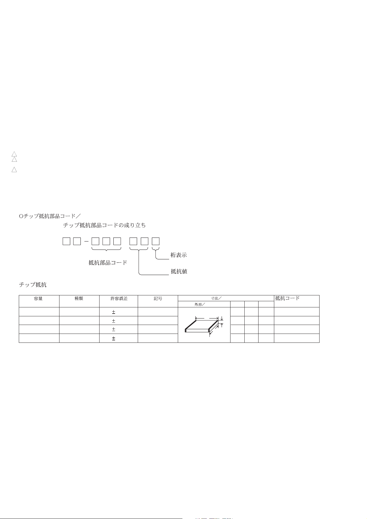
CHIP RESISTOR PART CODE
DESCRIPTIONREF. NO. KANRI
Chip Resistor Part Coding
88
A
Resistor Code
Chip resistor
Wattage Type Tolerance
1/16W 1005 5% CJ
1/16W
1/10W
1/8W
1608
2125
3216
5%
5%
5%
Symbol
CJ
CJ
CJ
Figure
Value of resistor
Form
L
Dimensions (mm)
t
W
0.55
Resistor Code
108
118
128
LW t
1.0 0.5 0.35 104
1.6 0.8 0.45
2 1.25 0.45
3.2
1.6
: A
: A
– 9 –
Page 10
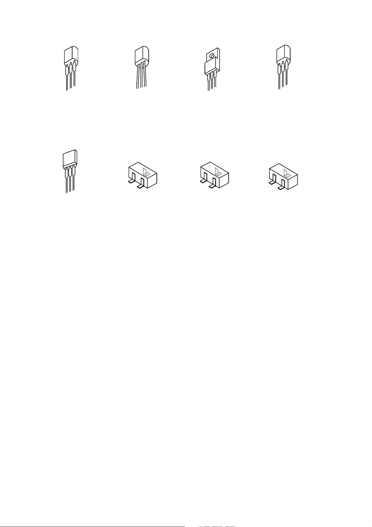
TRANSISTOR ILLUSTRATION
E C B
KTA1266GR
E C B
DTC114ES
2SC4115SRS
2SA933SRS
KTC3199GR
E C B
2SA1979O/Y
2SA1980G
2SC2240GR
2SC5342Y
CC5551
D
G
S
2SK2158
B C E
2SB1677
2SD2619
D
G
2SK360E
E C B
CSC4115BC
S
B
2SA1235F
2SC2714O
2SC3052F
2SC3326B
2SD1306E
CMBT5401
CSD1306E
DTA114EKA
C
E
DTC114TKA
KRA102S
KRC107S
KTA1504GR
KTC3875GR
RT1P141C
RT1P144C
SBT5401F
DTC114EKA
– 10 –
Page 11
WIRING – 1 (AMP – MICON) <U, EZ, K, HR>
32 31 30 29 28 27 26 25 24 23 22 21 20 19 18 17 16 15 14 13 12 11 10 9 8 7 6 5 4 3 2 1
A
B
C
D
E
F
G
H
I
J
K
L
M
N
O
P
Q
– 11 –
R
S
T
U
Page 12
WIRING – 2 (AMP – MICON) <C>
32 31 30 29 28 27 26 25 24 23 22 21 20 19 18 17 16 15 14 13 12 11 10 9 8 7 6 5 4 3 2 1
A
B
C
D
E
F
G
H
I
J
K
L
M
N
O
P
Q
– 12 –
R
S
T
U
Page 13
SCHEMATIC DIAGRAM – 1 (AMP – MICON)
– 13 –
Page 14
WIRING – 3 (FRONT / KEY / SUPPLY / MOSW / HP) <U, EZ, K>
32 31 30 29 28 27 26 25 24 23 22 21 20 19 18 17 16 15 14 13 12 11 10 9 8 7 6 5 4 3 2 1
A
B
C
D
E
F
G
H
I
J
K
L
M
N
O
P
Q
– 14 –
R
S
T
U
Page 15
WIRING – 4 (FRONT / KEY / SUPPLY / MOSW / HP) <HR, C>
32 31 30 29 28 27 26 25 24 23 22 21 20 19 18 17 16 15 14 13 12 11 10 9 8 7 6 5 4 3 2 1
A
B
C
D
E
F
G
H
I
J
K
L
M
N
O
P
Q
– 15 –
R
S
T
U
Page 16

SCHEMATIC DIAGRAM – 2 (FRONT / KEY / MOSW)
– 16 –
Page 17
SCHEMATIC DIAGRAM – 3 (SUPPLY / HP)
– 17 –
Page 18

WIRING – 5 (CD / JACK) <U, EZ, K>
32 31 30 29 28 27 26 25 24 23 22 21 20 19 18 17 16 15 14 13 12 11 10 9 8 7 6 5 4 3 2 1
A
B
C
D
E
F
G
H
I
J
K
L
M
N
O
P
Q
– 18 –
R
S
T
U
Page 19

WIRING – 6 (CD / JACK) <HR, C>
32 31 30 29 28 27 26 25 24 23 22 21 20 19 18 17 16 15 14 13 12 11 10 9 8 7 6 5 4 3 2 1
A
B
C
D
E
F
G
H
I
J
K
L
M
N
O
P
Q
– 19 –
R
S
T
U
Page 20

WIRING 7 (CD MOTOR)
151413121110987654321
K CD MOTOR C.B
M1
A
B
TO CD C.B CN2
+
<BLK>
6
5
3
<ORG>
1
PIN3
_
M1
C
(SLED MOTOR)
D
SW1
(INSIDE LIMIT SW)
E
F
M2
SW1
_
+
G
H
I
J
M2
(SPINDLE MOTOR)
K
PICK UP ASSY
SF-P101NR
16
1
FFC1
L
M
N
O
P
Q
R
S
T
20
U
TO CD C.B CN1
Page 21

SCHEMATIC DIAGRAM – 4 (CD 1 / 2 / CD – MOTOR)
– 21 –
Page 22

SCHEMATIC DIAGRAM – 5 (CD 2 / 2 / JACK)
– 22 –
Page 23

WIRING – 8 (PT) <U, EZ, K, C>
32 31 30 29 28 27 26 25 24 23 22 21 20 19 18 17 16 15 14 13 12 11 10 9 8 7 6 5 4 3 2 1
A
B
C
D
E
F
G
H
I
J
K
L
M
N
O
P
Q
– 23 –
R
S
T
U
Page 24

SCHEMATIC DIAGRAM – 6 (PT) <U, EZ, K, C>
– 24 –
Page 25

WIRING – 9 (PT) <HR>
32 31 30 29 28 27 26 25 24 23 22 21 20 19 18 17 16 15 14 13 12 11 10 9 8 7 6 5 4 3 2 1
A
B
C
D
E
F
G
H
I
J
K
L
M
N
O
P
Q
– 25 –
R
S
T
U
Page 26

SCHEMATIC DIAGRAM – 7 (PT) <HR>
– 26 –
Page 27

WIRING – 10 (TUNER) <U, HR, C>
15 14 13 12 11 10 9 8 7 6 5 4 3 2 1
A
B
C
D
E
F
G
H
I
J
K
L
M
N
O
P
Q
– 27 –
R
S
T
U
Page 28

SCHEMATIC DIAGRAM – 8 (TUNER) <U, HR, C>
– 28 –
Page 29

WIRING – 11 (TUNER) <EZ, K>
15 14 13 12 11 10 9 8 7 6 5 4 3 2 1
A
B
C
D
E
F
G
H
I
J
K
L
M
N
O
P
Q
– 29 –
R
S
T
U
Page 30

SCHEMATIC DIAGRAM – 9 (TUNER) <EZ, K>
– 30 –
Page 31

IC BLOCK DIAGRAM
– 31 –
Page 32

– 32 –
Page 33

LCD DIAGRAM
33
Page 34

IC DESCRIPTION
IC, LC78622NE
Pin No.
1 DEFI I Defect detection signal (DEF) input. ("L" is applied when not used.)
2 TAI I For PLL/Test input. (Connected to 0V)
3 PDO O Phase comparison output to control the external VCO.
4 VVSS – Ground of the built-in VCO. Normally 0V.
5 ISET I For the connection of a resistor which adjusts the PDO output current.
6 VVDD – Power supply of the built-in VCO.
7 FR I Adjusts the VCO frequency range.
8 VSS – Ground of digital circuits. Normally 0V.
9 EFMO O For slice level control/EFM signal output.
10 EFMIN I EFM signal input.
11 T2 I Test input. A pull-down resistor is incorporated. (Connected to 0V)
12 CLV+
13 CLV-
14 V/P O
15 HFL I Track detection signal input. Schmitt trigger input.
16 TES I Track error signal input. Schmitt trigger input.
17 TOFF O Tracking off output.
Pin Name I/O
O Disc motor control tri-state output.
Output to monitor the automatic switching between the rough servo control and phase servo
control. "H" : Rough servo, "L": Phase servo.
Description
18 TGL O Tracking gain switching output. "L" raises the gain.
19 JP+
20 JP-
21 PCK O
22 FSEQ O
23 VDD – Power supply of digital circuits.
24 SL+ O Controlled by serial data command issued by the microprocessor.
25 SL– O Controlled by serial data command issued by the microprocessor.
26 NC – Not connected.
27 PU IN I CD pickup inside limit switch.
28 CD R/W O CD-RW disc select control.
29 EMPH O Deemphasis monitor. "H": when playing a deemphasis disc. (Not used)
30 C2F O C2 flag output. (Not used)
31 DOUT O Output a digital OUT signal. (EIAJ format) (Not used)
32 T3
33 T4
O Track jump control tri-state output.
Monitors the clock signal for EFM data playback. 4.3218MHz when the phase is locked.
(Not used)
Sync signal detection output. Goes "H" when the sync signal detected from the EFM
signal matches the sync signal generated internally. (Not used)
I Test input. (Connected to 0V)
34 NC – Not connected.
35 MUTEL O Lch 1-bit DAC/Lch muting output. (Not used)
36 LVDD – Lch power supply.
37 LCHO O Lch output.
38 LVSS – Lch ground. Normally 0V.
– 34 –
Page 35

Pin No.
39 RVSS – Rch 1-bit DAC/Rch ground. Normally 0V.
40 RCHO O Rch output.
41 RVDD – Rch power supply.
42 MUTER O Rch muting output. (Not used)
43 XVDD – Power supply of crystal oscillator.
44 XOUT O
45 XIN I
46 XVSS – Ground of crystal oscillator. Normally 0V.
47 SBSY O Subcode block sync signal output. (Not used)
48 EFLG O C1, C2, single, duplex correction monitor. (Not used)
49 PW O Output of subcodes P, Q, R, S, T, U and W. (Not used)
50 SFSY O Subcode frame sync signal output. Falls when the subcode is set to the standby state. (No used)
Pin Name
I/O Description
For the connection of a 16.93MHz crystal oscillator.
51 SBCK I
52 FSX O 7.35kHz sync signal output obtained by dividing the oscillator frequency. (Not used)
53 WRQ O Subcode Q standby output.
54 RWC I Read/write control input. Schmitt trigger input.
55 SQOUT O Subcode Q output.
56 COIN I Command input from the microprocessor.
57 CQCK I
58 RES I LC78622NE reset input.
59 T11 O Test output. Set to open (normally "L" output.) (Not used)
60 16M O 16.9344MHz output. (Not used)
61 4.2M O 4.236MHz output.
62 T5 I Test input. A pull-down resistor is incorporated. (Connected to 0V)
63 CS I Chip select input. (Connected to 0V)
64 T1 I Test input with no pull-down resistor. (Connected to 0V)
Subcode read-out clock input. Schmitt trigger input. ("L" is applied when not used.)
(Connected to 0V)
Command input retrieval clock or subcode retrieval clock input from SQOUT. Schmitt trigger
input.
– 35 –
Page 36

IC, LA9241ML
Pin No.
1 FIN2 I
2 FIN1 I For the connection of the pickup photodiode.
3EI
4 F I For the connection of the pickup photodiode.
5 TB I Inputs the DC components in the TE signal.
6 TE– I
7 TE O TE signal output.
8 TESI I TES (track error sense) comparator input. The TE signal is passed through a BPF.
9 SCI I Shock detection input.
10 TH I Sets the time constant for the tracking gain.
11 TA O TA amp output.
12 TD– I Composes the tracking phase compensation constant between the TD and VR pins.
13 TD O Sets the tracking phase compensation.
14 JP I Sets the amplitude of the tracking jump signal (kick pulses).
Pin Name I/O
For the connection of the pickup photodiode. Addition to the FIN1 pin creates an RF
signal and subtraction from it create an EF signal.
For the connection of the pickup photodiode. Subtraction from the F pin creates a TE
signal.
For the connection of a resistor which sets the gain of the TE signal between this pin
and the TE pin.
Description
15 TO O Tracking control signal output.
16 FD O Focusing control signal output.
17 FD– I Composes the focusing phase compensation constant between the FD and FA pins.
18 FA O Composes the focusing phase compensation constant between the FD- and FA- pins.
19 FA– I Composes the focusing phase compensation constant between the FA and FE pins.
20 FE O FE signal output.
21 FE– I
22 A-GND – Ground of analog signals.
23 SP O Single-ended output of the signals input to the CV+ and CV- pins.
24 SPI I Spindle amp input.
25 SPG I For the connection of a resistor which sets the gain in the spindle 12cm mode. (Not used)
26 SP– I For the connection of the spindle phase compensation constant with the SPD pin.
27 SPD O Spindle control signal output.
28 SLEQ I For the connection of sled phase compensation constant.
29 SLD O Sled control signal output.
30 SL–
31 SL+
For the connection of a resistor whichs sets the gain of the FE signal between this pin
and the TE pin.
I Sled feed signal input from the microprocessor.
32 JP–
33 JP+
34 TGL I Tracking gain control signal input from the DSP. Low gain when TGL is "H".
35 TOFF I Tracking off control signal input from the DSP. Off when TOFF is "H".
36 TES O Outputs the TES signal to the DSP.
I Tracking signal input from the DSP.
– 36 –
Page 37

Pin No.
37 HFL O
38 SLOF I Sled servo off control input.
I/O DescriptionPin Name
The HFL (high frequency level) signal is used to judge whether the main beam is positioned on
the pit or on the mirror.
39 CV–
40 CV+
41 RFSM O RF output.
42 RFS– O Sets the RF gain and the EFM signal's 3T compensation constant together with the RFSM pin.
43 SLC O
44 SLI I Input to control the DSP's data slice level.
45 D-GND – Ground of digital signals.
46 FSC O Output for the focus search smoothing capacitor.
47 TBC I The TBC (tracking balance control) signal sets the EF balance variation range.
48 NC – Not connected.
49 DEF O Disc defect detection output.
50 CLK I Reference clock input. 4.23MHz is input from the DSP.
51 CL I Microprocessor command clock input.
52 DAT I Microprocessor command data input.
53 CE I Microprocessor chip enable input.
54 DRF O DRF (detect RF) is an output to detect the RF level.
55 FSS I
I CLV error signal input from the DSP.
The SLC (slice level control) signal is output to control the DSP's data slice level of the RF
waveform.
The FSS (focus search select) signal switches the focus search modes (+/-search / +search with
respect to the reference voltage). (Not used)
56 VCC2 – VCC of servo and digital circuits.
57 REFI – For the connection of bypass capacitor for the reference voltage.
58 VR O Reference voltage output.
59 LF2 – Sets the time constant for disc defect detection.
60 PH1 – For the connection of a capacitor to hold the RF signal peak.
61 BH1 – For the connection of a capacitor to hold the RF signal bottom.
62 LDD O APC circuit output.
63 LDS I APC circuit input.
64 VCC1 – VCC of RF signal circuits.
– 37 –
Page 38

IC, LC876564V-5V69
Pin No. Pin Name I/O Description
1
O-CD CLK
O
CD IC control clock output.
10
11
12
13
14
15
16
17
18
2
3
4
5
6
7
8
9
O-CD CE
I-CD WRQ
I-CD DRF
I-CD SUBQ
O-CD ON
O-MUTE
O-POWER
O-TUNE ON
O-CLK SHIFT
RESET
I-HOLD
I-LEVEL (NC)
VSS1
CF1
CF2
VDD1
O-AMP ON
O
CD IC control chip enable output.
I
Input standby for CD subcode Q output.
I
Detect CD RF level.
I
CD IC data input.
O
CD ON / OFF control output.
O
Audio mute ON / OFF control output.
O
System power supply ON/ OFF output.
O
Tuner ON / OFF control output.
O
MICON clock shift output.
I
Reset input.
I
Power failure detection input.
I
Signal level input. (Not used)
-
GND.
-
9.43MHz oscillator circuit.
-
9.43MHz oscillator circuit.
-
Power supply input.
O
AMP ON / OFF control output. (Not used)
19
20
21
22
23
24
25
26
27
28
29
30 ~ 45
46
47 ~ 50
51
52 ~ 71
72
O-PLL CE
I-TUNE/IFC
I-STEREO
I-RDS DATA
I-TUNER
I-KEY1
I-KEY2
I-RDS CLK
I-TU SIG
I-TM BASE
I-REMOCON
NC
VDD3
NC
VP
NC
VDD4
O
PLL IC chip enable output.
I
IF count serial data input.
I
Tuner stereo detect input.
I
RDS data input. <EZ only>
I
Tuner select input. (A /D)
I
Key input. (A /D)
I
Key input. (A /D)
I
RDS clock input. <EZ only>
I
Tuner SD detect input. <EZ only>
I
Reference clock input for watch.
I
System remote control signal input.
-
Not connected.
-
Power supply input.
-
Not connected.
-
GND.
-
Not connected.
-
Power supply input.
73 ~ 76
77
78
79
80
81
82 ~ 84
NC
O-BLU LED
O-RED LED
O-GRN LED
NC
OSC
NC
-
Not connected.
O
Blue LED control output.
O
Red LED control output.
O
Green LED control output.
-
Not connected.
-
OSC test point.
-
Not connected.
– 38 –
Page 39

Pin No. Pin Name I/O Description
85
O-DATA
O PLL, function IC control data output.
86
87
88
89
90
91
92
93
94
95
96
97
98
99
100
O-CLK
O-FUNC CE
O-STANDBY
VSS2
VDD2
I-JOG1
I-JOG2
I-CD OPEN
I-CD CLOSE
O-CD OPEN
O-CD CLOSE
O-CD DATA
O-LCD DATA
O-LCD CE
O-LCD CLK
O PLL, function IC control clock output.
O Function IC control chip enable output.
O Standby LED ON / OFF control output.
- GND.
- Power supply input.
I Jog signal input.
I Jog signal input.
I CD open switch signal input.
I CD close switch signal input.
O CD cover open signal output.
O CD cover close signal output.
O CD IC control data output.
O LCD control data output.
O LCD control chip enable output.
O LCD control clock output.
– 39 –
Page 40

ADJUSTMENT <TUNER / CD / AMP – MICON>
< TUNER SECTION > <U, C>
1. Clock Frequency Check
Settings : • Test point : TP2(CLK)
Method : Set to AM 1710kHz and check that the test point is
2160kHz ± 45Hz.
2. AM VT Check
Settings : • Test point : TP1(VT)
Method : Set to AM 1710kHz and check that the test point is less
than 8.5V. Then set to AM 530kHz and check that the
test point is more than 0.6V.
3. AM Tracking Adjustment
Settings : • Test point : TP8(Lch), TP9(Rch)
• Adjustment location : L981(1/3)
Method : Set to AM 1000kHz and adjust L981(1/3) so that the
test point becomes maximum.
4. AM IF Adjustment
Settings : • Test point : TP8(Lch), TP9(Rch)
• Adjustment location :
L772 ............................................................ 450kHz.
5. FM VT Check
Settings : • Test point : TP1(VT)
Method : Set to FM 108.0MHz and check that the test point
is less than 8.0V. Then set to FM 87.5MHz and check
that the test point is more than 0.5V.
7. DC Balance / Mono Distortion Adjustment
Settings : • Test point : TP3, TP4 (DC Balance)
TP8(Lch), TP9(Rch) (Distortion)
• Adjustment location : L771
• Input level : 60dBµV
Method : Set to FM 98.0MHz and adjust L771 so that the voltage
between TP3 and TP4 becomes 0V ± 0.04V. Then check
that the distortion is less than 1.3%.
8. Output Level Check
<AM>
Settings : • Test point : TP8(Lch), TP9(Rch)
• Input level : 74dBµV
Method : Set to AM 1000kHz and check that the test point is
175mV ± 3dB.
<FM>
Settings : • Test point : TP8(Lch), TP9(Rch)
• Input level : 60dBµV
Method : Set to FM 98.0MHz and check that the test point is
700mV ± 3dB.
9. FM Seperation Check
Settings : • Test point : TP8(Lch), TP9(Rch)
• Input level : 60dBµV
Method : Set to FM 98.0MHz and check that the test point is
more than 25dB.
6. FM Tracking Check
Settings : • Test point : TP8(Lch), TP9(Rch)
Method : Set to FM 98.0MHz and check that the test point is less
than 9dBµV.
– 40 –
Page 41

< TUNER SECTION > <EZ, K>
1. Clock Frequency Check
Settings : • Test point : TP2(CLK)
Method : Set to MW 1602kHz and check that the test point is
2052kHz ± 45Hz.
2. MW VT Check
Settings : • Test point : TP1(VT)
Method : Set to MW 1602kHz and check that the test point is less
than 8.0V. Then set to MW 531kHz and check that the
test point is more than 0.6V.
3. MW Tracking Adjustment
Settings : • Test point : TP8(Lch), TP9(Rch)
• Adjustment location : L981(1/3)
Method : Set to MW 999kHz and adjust L981(1/3) so that the
test point becomes maximum.
4. LW VT Adjustment
Settings : • Test point : TP1(VT)
• Adjustment location : L942
Method : Set to LW 144kHz and adjust L942 so that the test point
becomes 1.3V ± 0.05V. Then set to LW 290kHz and
check that the test point is less than 8.0V.
5. LW Tracking Adjustment
Settings : • Test point : TP8(Lch), TP9(Rch)
• Adjustment location :
L941 ............................................................ 144kHz.
TC942 .......................................................... 290kHz.
Method : Set up TC942 to center before adjustment.
Adjust L941 so that the level at 144kHz becomes
maximum. Then adjust TC942 so that the level at
290kHz becomes maximum.
8. FM Tracking Check
Settings : • Test point : TP8(Lch), TP9(Rch)
Method : Set to FM 98.0MHz and check that the test point is less
than 9dBµV.
9. DC Balance / Mono Distortion Adjustment
Settings : • Test point : TP3, TP4 (DC Balance)
TP8(Lch), TP9(Rch) (Distortion)
• Adjustment location : L771
• Input level : 60dBµV
Method : Set to FM 98.0MHz and adjust L771 so that the voltage
between TP3 and TP4 becomes 0V ± 0.04V. Then check
that the distortion is less than 1.3%.
10. Output Level Check
<AM>
Settings : • Test point : TP8(Lch), TP9(Rch)
• Input level : 74dBµV
Method : Set to AM 1000kHz and check that the test point is
175mV ± 3dB.
<FM>
Settings : • Test point : TP8(Lch), TP9(Rch)
• Input level : 60dBµV
Method : Set to FM 98.0MHz and check that the test point is
700mV ± 3dB.
11. FM Seperation Check
Settings : • Test point : TP8(Lch), TP9(Rch)
• Input level : 60dBµV
Method : Set to FM 98.0MHz and check that the test point is
more than 25dB.
6. AM IF Adjustment
Settings : • Test point : TP8(Lch), TP9(Rch)
• Adjustment location :
L772 ............................................................ 450kHz.
7. FM VT Check
Settings : • Test point : TP1(VT)
Method : Set to FM 108.0MHz and check that the test point is less
than 8.0V. Then set to FM 87.5MHz and check that the
test point is more than 0.5V.
– 41 –
Page 42

< TUNER SECTION > <HR>
1. Clock Frequency Check
Settings : • Test point : TP2(CLK)
Method : Set to AM 1602kHz and check that the test point is
2052kHz ± 45Hz.
2. AM VT Check
Settings : • Test point : TP1(VT)
Method : Set to AM 1602kHz and check that the test point is less
than 8.0V. Then set to AM 531kHz and check that the
test point is more than 0.6V.
3. AM Tracking Adjustment
Settings : • Test point : TP8(Lch), TP9(Rch)
• Adjustment location : L981(1/3)
Method : Set to AM 999kHz and adjust L981(1/3) so that the
test point becomes maximum.
4. AM IF Adjustment
Settings : • Test point : TP8(Lch), TP9(Rch)
• Adjustment location :
L772 ............................................................ 450kHz.
5. FM VT Check
Settings : • Test point : TP1(VT)
Method : Set to FM 108.0MHz and check that the test point
is less than 8.0V. Then set to FM 87.5MHz and check
that the test point is more than 0.5V.
7. DC Balance / Mono Distortion Adjustment
Settings : • Test point : TP3, TP4 (DC Balance)
TP8(Lch), TP9(Rch) (Distortion)
• Adjustment location : L771
• Input level : 60dBµV
Method : Set to FM 98.0MHz and adjust L771 so that the voltage
between TP3 and TP4 becomes 0V ± 0.04V. Then check
that the distortion is less than 1.3%.
8. Output Level Check
<AM>
Settings : • Test point : TP8(Lch), TP9(Rch)
• Input level : 74dBµV
Method : Set to AM 1000kHz and check that the test point is
175mV ± 3dB.
<FM>
Settings : • Test point : TP8(Lch), TP9(Rch)
• Input level : 60dBµV
Method : Set to FM 98.0MHz and check that the test point is
700mV ± 3dB.
9. FM Seperation Check
Settings : • Test point : TP8(Lch), TP9(Rch)
• Input level : 60dBµV
Method : Set to FM 98.0MHz and check that the test point is
more than 25dB.
6. FM Tracking Check
Settings : • Test point : TP8(Lch), TP9(Rch)
Method : Set to FM 98.0MHz and check that the test point is less
than 9dBµV.
– 42 –
Page 43

< CD SECTION >
CD PWB
Q1
CD Adjustment Method
• Perform the adjustments after the machine enters the test mode.
• Place the CD mechanism on level ground.
• Equipment and tools required
Measuring equipment: Oscilloscope (Use the probe of 10:1)
Test Disc: TCD-782
1. Focus Bias Adjustment
1) Connect a digital multimeter to the test point (FE), (VC).
2) Play back the 2nd track of TCD-782.
3) Adjust SFR130 until the digital multimeter indicates 0 ± 10 mV.
2. RF Waveform Check
1) Connect an oscilloscope to test point (RF), (VC).
2) Play back the 2nd track of TCD-782.
3) Check that the RF waveform has the maximum amplitude and
the center of the wedge waveform has the clear blank.
3. Jitter Check
1) While an oscilloscope is kept connected in the same test point as
in step 2. RF Waveform Check, connect the output terminal of an
oscilloscope to the input terminal of the jitter meter.
2) Set the VOLT range selector of an oscilloscope to 500 mV range
or lower.
3) Play back the 2nd track of TCD-782.
4) Check that the jitter meter indicates 28.0 ns or less.
4. Play Ability Check
1) Play back the 3rd, 8th, and 13th track of ATD-001. Check that the
noise does not occur and sound skipping does not occur.
R2
IC1
PATTERN SIDE
IC2
RF
R35
R40
IC501
IC120
2
5
Digital Multimeter (Use it in the DC Volt range)
Jitter meter (Kikusui 6235)
ATD-001
PARTS SIDE
3
VC
DIGITAL MULTIMETER
FE
VC
OSCILLOSCOPE
OUTPUT
RF
VC
RF
VC
SFR130
JW12
EYE PATTERN
must be CLEAR and MAX
OSCILLOSCOPE
JW13
FE
V
OUTPUT
1
3
2
1
INPUT
VOLT / DIV: 500mV
TIME / DIV: 0.2µs
JITTER METER
ns
Approx.
1.8Vp-p
0V
5. Laser Current Check
* Do not perform this measurement unless the laser is suspected to
be defective.
1) Connect a digital multimeter across the resistor R2 (10 Ω).
2) Play back the TCD-782 and check the DC voltage value on the
digital multimeter.
3) Calculate the laser current (Iop) by dividing the DC voltage across
R2 by the resistor value (R2 = 10 Ω). Check that the laser current
(Iop) is 80 mA or less.
DIGITAL MULTIMETER
V
R2
R2
– 43 –
Page 44

< AMP – MICON SECTION >
AMP-MICON PWB
PATTERN SIDE
IC301
OSC (81pin)
GND (51pin)
1. Clock Adjustment
1) Connect an oscilloscope to test point OSC (IC301 81 pin) and GND (IC301 51 pin).
2) Insert the AC plug while pressing POWER and TUNER / BAND buttons.
3) Adjust L151 until the oscilloscope indicates 97.250 ± 0.050Hz (10.278 ~ 10.288ms)
PARTS SIDE
CN401
L151
– 44 –
Page 45

CD TEST MODE
1. How to Start the CD Test Mode
While pressing the CD FUNCTION button, insert the AC plug to the power outlet.
When the test mode started, all lights on the display are lit.
2. How to Exit the CD Test Mode
Press the POWER button or press the other FUNCTION buttons or disconnect the AC plug.
3. Function and Usage of the CD Test Mode
No Mode
1 Start Mode All lights are FL check
2 Search Mode PLAY button Normal LD illuminates all the time APC circuit check
(without disc) Focus search continues Laser current measurement
3 Play Mode PLAY button Normal Normal playback Each servo circuit is checked
4 Sled Mode FF button Pickup moves to the inner Sled circuit check
* 1. The driver IC heats up and the protection circuit starts working when the focus search is continued for 10 minutes or longer. There can be a
case that operations cannot be performed correctly. In such a case, turn off the main power. After cooling down the machine, restart the
machine.
* 2. Be careful not to damage the gear because the sled motor rotates while the FF or RWD button is being pressed even if the pickup is located in
the innermost track or the outermost track.
Button for
Activation
RWD button Pickup is moves to the outer
Display Operation Contents
lit. Microcomputer check
operations *1 Focus search waveform check
Spindle motor continuous kick Focus error waveform check
If TOC cannot be read, focus DRF check
search is continued
circumference *2 Mechanism operation check
circumference *2
(DRF in the search mode is ignored)
Pickup check
45
Page 46

MECHANICAL PARTS ARRANGEMENT 1 / 6
C
x3
A
x3
D
x4
SH,ADH TOP
1
G
SH,RING TOP
3
2
6
F
x2
B
x2
PWB
5
55
B
COVER,
HT-SINK
x2
46
B
x11
4
B
x3
Page 47

MECHANICAL PARTS ARRANGEMENT 2 / 6
7
9
B
11
8
10
B
x3
B
x9
PWB
53
54
13
12
47
Page 48

MECHANICAL PARTS ARRANGEMENT 3 / 6
22
PWB
53
21
17
G
x2
20
18
19
H
PWB
I
H
23
15
14
16
48
Page 49

MECHANICAL PARTS ARRANGEMENT 4 / 6
TERMINAL,LB 4 NI
HT-SINK,
ASSY MAIN
B
x5
B
x5
PWB
B
HT-SINK,TR MAIN
B
x4
27
27
x4
K
J
DA11B3
28
32
32
49
Page 50

MECHANICAL PARTS ARRANGEMENT 5 / 6
HT-SINK,TR SUB
B
x4
B
B
x2
PWB
24
33
B
x6
34
29
PWB
25
COVER,WIRE(TP)
PWB
32
30
29
B
26
WIRE ASSY, LUG-5
E
PWB
O
x4
29
35
M
x4
31
44
32
56
36
K MODEL
50
Page 51

MECHANICAL PARTS ARRANGEMENT 6 / 6
B
x2
39
38
37
47
E
x4
N
B
x4
N
51
LCD
D
x4
SH,DIFFUSION
49
J
x4
48
45
PWB
42
SH,LCD
52
41
40
50
46
L
PWB
43
51
Page 52

MECHANICAL PARTS LIST 1 / 1
PART NO.
1 8B-CL2-009-010 CAP, TOP
2 8B-CL2-054-010 WINDOW,TOP(N)<K,EZ,HR>
2 8B-CL2-055-010 WINDOW,TOP(N) U <U,C>
3 8B-CL2-045-110 RING,TOP
4 8B-CL2-022-110 PANEL,REAR CSM<C>
4 8B-CL2-028-110 PANEL,REAR USM<U>
4 8B-CL2-030-110 PANEL,REAR KSM<K>
4 8B-CL2-031-110 PANEL,REAR EZSM<EZ>
4 8B-CL2-032-110 PANEL,REAR HRJSM<HR>
5 88-912-081-110 FF-CABLE,12P 1.25 80MM
6 87-A90-796-010 FAN,F614R-12MC-19-240MM
7 8A-CQU-043-010 CUSH,TOP
8 8B-CL2-005-210 CABI,TOP U<U,C>
8 8B-CL2-040-210 CABI,TOP<K,EZ,HR>
9 8B-CL2-012-110 PLATE,OPE(L2)
10 8B-CL2-014-110 ARM,OPEN L
11 8B-CL2-223-010 HLDR,ARM L
12 8B-CL2-047-010 KEY,PLAY
13 8B-CL2-044-010 KEY,FUN
14 87-A90-036-010 MOT ASSY,RF-300CA-11440
15 84-ZG1-267-010 PULLEY,LOAD MO 8
16 8B-CL2-211-110 CHAS,GEAR
17 8B-CL2-214-010 GEAR,PULLY
18 8B-CL2-225-010 BELT,SQ1.2-32.2
19 8B-CL2-215-010 GEAR,MIDDLE
20 8B-CL2-226-010 W-P,6.5-12.8-0.3 B W/O ADH
21 8B-CL2-216-010 GEAR,OUT
22 8B-CL2-013-110 ARM,OPEN R
23 8B-CL2-212-010 HLDR,GEAR
24 8B-CL2-662-010 FF-CABLE,11P 1.0
25 8B-CL2-661-010 FF-CABLE,9P 1.0
26 88-908-121-110 FF-CABLE,8P 1.25 120MM
27 88-CH6-220-110 CUSHION,CD A
28 8Z-CDB-169-010 PANEL,CD SANYO
29 87-064-185-010 HLDR,WIRE PVC 0.5<K,EZ,HR>
30 88-NF9-203-010 BUSHING,CORD-U<U,C>
30 88-NF9-210-010 BUSHING,CORD-E<K,EZ,HR>
31 87-A80-092-010 AC CORD ASSY,E BLK SUN FAI<EZ>
!
31 87-A80-143-010 AC CORD ASSY,E BLK<K,HR>
!
31 87-A80-149-010 AC CORD ASSY,U BLK<U,C>
!
32 87-A90-193-010 HLDR,CV100 (B)
33 86-ZG1-609-010 CONN ASSY,6P
34 8B-CL2-663-010 FF-CABLE,16P 1.0
35 8B-CL2-201-110 HLDR,PT
!
36 8B-CL2-650-010 PT,BCL-2 U<U>
NO.
DESCRIPTIONREF. NO. KANRI
PART NO.
!
36 8B-CL2-652-010 PT,BCL-2 EZ<K,EZ>
36 8B-CL2-653-010 PT,BCL-2 HR<HR>
!
36 8B-CL2-654-010 PT,BCL-2 C<C>
!
37 8B-CL2-010-010 WINDOW,FR
38 8B-CL2-026-010 REFLECTOR,VOL
39 8B-CL2-025-010 KNOB,RTRY VOL
40 8B-CL2-048-010 KEY,POWER
41 8B-CL2-027-010 REFLECTOR,POWER
42 8B-CL2-049-010 KEY,JOG
43 8B-CL2-001-010 CABI,FR<K,HR>
43 8B-CL2-004-010 CABI,FR U<U,C>
43 8B-CL2-008-010 CABI,FR EZ<EZ>
44 87-003-317-010 F-BEAD,15-25-15 E2515MRT
45 8B-CL2-218-010 HLDR,LCD R
46 8B-CL2-219-010 HLDR,LCD L
47 8B-CL2-041-110 CABI,BOTTOM<K>
47 8B-CL2-042-110 CABI,BOTTOM EZ<EZ>
47 8B-CL2-006-110 CABI,BOTTOM U<U,C>
47 8B-CL2-007-110 CABI,BOTTOM HR<HR>
48 8B-CL2-043-110 FOOT,ARCH
49 8B-CL2-205-110 HLDR,FOOT
50 8B-CL2-220-010 GUIDE,LCD
51 8B-CL2-029-010 REFLECTOR,LCD
52 8B-CL2-660-010 FF-CABLE,21P 1.0
53 88-905-121-110 FF-CABLE, 5P 120MM
54 88-908-201-110 FF-CABLE,8P 1.25
55 88-904-081-110 FF-CABLE,4P 1.25 80MM<EZ>
56 87-099-811-010 PLUG,ADPTR CONV(K)<K>
!
A 87-067-761-010 BVT2+3-10 BLK
B 87-067-703-010 BVT2+3-10 W/0 SL0T
C 8A-NF7-251-010 W,3.2-8-0.45
D 8Z-CL1-034-010 S-SCREW,ZCL1
E 87-067-579-010 BVT2+3-8 W/O SLOT
F 87-067-822-010 BVT2+3-20 W/0 SL0T
G 87-067-868-010 V+1.7-4 BLK HL
H 87-B10-294-010 BVT2+2.6-8
I 87-067-767-010 BVTT+2.6-6
J 87-067-584-010 BVT2+3-6 W/0 SL0T
K 8Z-CK5-222-010 S-SCREW,CD+2.6-6 F9
L 88-AR1-217-010 S-SCREW,BFT2+3-8
M 87-067-585-010 BVTT+4-6
N 87-721-095-410 QT2+3-8 W/O SL0T
O 87-741-096-410 UT2+3-10 W/O SLOT
NO.
DESCRIPTIONREF. NO. KANRI
COLOR NAME TABLE
Basic color symbol Color Basic color symbol Color Basic color symbol Color
B Black C Cream D Orange
G Green H Gray L Blue
LT Transparent Blue N Gold P Pink
R Red S Silver ST Titan Silver
T Brown V Violet W White
WT Transparent White Y Yellow YT Transparent Yellow
LM Metallic Blue LL Light Blue GT Transparent Green
LD Dark Blue DT Transparent Orange GM Metallic Green
YM Metallic Yellow DM Metallic Orange PT Transparent Pink
LA Aqua Blue GL Light Green HT Transparent Gray
52
Page 53

CD MECHANISM EXPLODED VIEW 1 / 1
1
SW1
M2
A
2
3
4
PWB
CD MECHANISM PARTS LIST 1 / 1
REF. NO. DESCRIPTIONPART NO.
1 M8-AZK-M90-070 DA11B3
2 S2-121-A28-400 COVER GEAR
3 S2-511-A21-000 GEAR MIDDLE
4 S2-511-A21-100 GEAR,DRIVE
A S1-PN2-03R-OSE SCR PAN PCS 2-3
KANRI
NO.
M1
PIN 3
– 53 –
Page 54

SPEAKER DISASSEMBLY INSTRUCTIONS
SX-LX7
1. Remove the speaker net.
2. Remove the four screws 1 .
4. Take out the rubber bushes 2 , then remove the screws hidden by the bushes.
2
2
5. Remove the front panel.
2
2
1
1
3. Remove the woofer.
1
1
6. Remove the two screws and tweeter.
3
3
54
Page 55

SPEAKER PARTS LIST <SX LX7 (YJSN, YUJSN)>
PART NO.
NO.
1 8B-CP2-001-010 PANEL,FR
2 8B-CP2-002-010 PANEL,REAR
3 8B-CP2-003-010 CABI,S
4 8B-CP2-004-010 PANEL,DUCT A
5 8B-CP2-005-010 PANEL,DUCT B
6 8B-CP2-007-010 GRILLE,FRAME ASSY
7 8B-CP2-016-010 GRILLE,FRAME ASSY L/GR<YUJSN>
8 8B-CP2-018-010 GRILLE,FRAME ASSY D/GR<YUJSN>
9 8B-CP2-015-010 RING,W
10 8B-CP2-011-010 RING,TW
11 8B-CP2-012-010 TERMINAL
12 8B-CP2-013-010 FOOT
13 8A-CJ5-411-010 SPKR,W 87S
14 8B-CP2-604-010 SPKR,TW 25
15 8B-CP2-614-010 CORD,SP
16 8B-CP2-020-010 HLDR,A
17 8B-CP2-021-010 HLDR,B
DESCRIPTIONREF. NO. KANRI
ACCESSORIES / PACKAGE LIST
PART NO.
1 8B-CL2-903-210 IB,U(ESF)M<U,C>
1 8B-CL2-901-010 IB,H(ECA)M<HR>
1 8B-CL2-905-010 IB,K(E)M<K>
1 8B-CL2-906-110 IB,EZ(9L)M<EZ>
2 87-006-225-010 ANT,LOOP ANT NC2
3 87-043-115-010 FEEDER-ANT,FM<U,HR,C>
3 87-A90-118-010 ANT,WIRE FM(Z)<EZ,K>
4 8B-CL2-961-010 RC UNIT,RC-BAT01(BS)
5 87-A92-262-010 PLUG,CONVERSION WT01<HR>
!
!
6 87-099-811-010 PLUG,ADPTR CONV(K)<K>
NO.
DESCRIPTIONREF. NO. KANRI
55
Page 56

2–11, IKENOHATA 1–CHOME, TAITO-KU, TOKYO 110, JAPAN TEL:03 (3827) 3111
9301978 931261
Printed in Singapore
 Loading...