

Page 1
XR-MR5
HR
SERVICE MANUAL
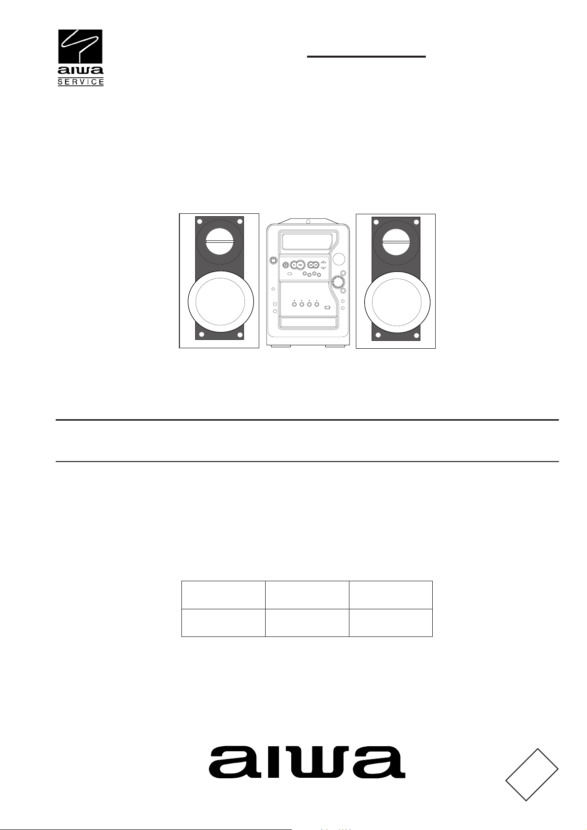
CD-R/CD STEREO SYSTEM
SYSTEM SPEAKERS
XR–MR5 RC–AAT16
BASIC CD MECHANISM : DA11B3
BASIC CD-R/RW MECHANISM : CRD-RA1W02(A)
REMOTE
CONTROLLER
SX–M510
S/M Code No. 09-00B-435-4N2
DATA
Page 2

SPECIFICATIONS
Main unit
<FM Tuner section>
Tuning range 87.5 MHz to 108 MHz
Usable sensitivity (IHF) 13.2 dBf
Antenna terminal 75 ohms (unbalanced)
<AM Tuner section>
Tuning range 531 kHz to 1602 kHz (9 kHz step)
530 kHz to 1710 kHz (10 kHz step)
Usable sensitivity 350 µV/m
Antenna Loop antenna
<Amplifier section>
Power output 25 W + 25 W (6 ohms, THD 1 %, 1 kHz)
30 W + 30 W (6 ohms, THD 10 %, 1 kHz)
Inputs AUX/VIDEO IN: 310 mV
DIGITAL IN
Outputs SPEAKERS:
accept speakers of 6 ohms or more
PHONES (stereo mini jack): accept
headphones of 32 ohms or more
<Compact disc player section (CD player)>
Laser Semiconductor laser (λ =780 nm)
D-A converter 1 bit dual
Signal-to-noise ratio 85 dB (1 kHz, 0 dB)
Harmonic distortion 0.05 % (1 kHz, 0 dB)
Wow and flutter Unmeasurable
<Compact disc recorder section (CD-R/RW player/recorder)>
Laser Semiconductor laser (λ =785 ± 5 nm)
Recording method Track at once
Sampling frequency 44.1 kHz
Harmonic distortion Play: 0.05 % or less (1 kHz, 0 dB)
Digital record: 0.05 % or less
(1 kHz, 0 dB)
<General>
Power requirements 120 V / 220-240 V AC, switchable,
50/60 Hz
Power consumption 90 W
Standby power consumption 1.5 W (power-economizing mode
set to ON or AUTO)
Dimensions of main unit 177.6 x 265.0 x 333.0 mm
(W x H x D)
Weight of main unit 6.0 kg
Speaker system
Cabinet type 2 way, bass reflex
(magnetic shielded type)
Speakers Woofer: 130 mm
Tweeter: 22 mm dome type
Impedance 6 ohms
Output sound pressure level 86 dB/W/m
Dimensions (W x H x D) 155 x 254 x 210 mm
Weight 2.6 kg
• Design and specifications are subject to change without notice.
• The word "BBE"and the "BBE symbol" are trademarks of BBE
Sound, Inc.
Under license from BBE Sound,Inc.
– 2 –
Page 3
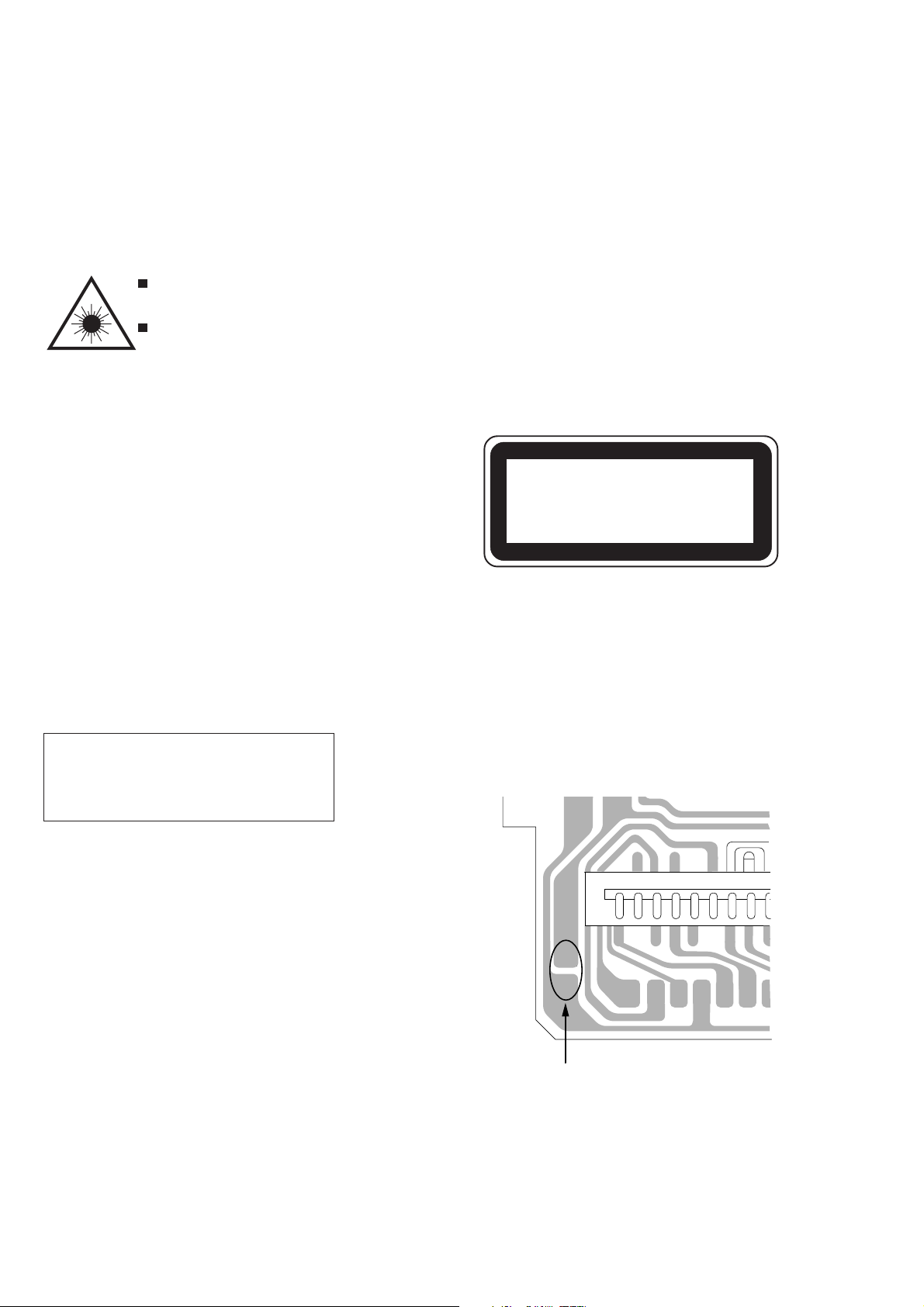
PROTECTION OF EYES FROM LASER BEAM DURING SERVICING
This set employs laser. Therefore, be sure to follow carefully the
instructions below when servicing.
WARNING!!
WHEN SERVICING, DO NOT APPROACH THE LASER
EXIT WITH THE EYE TOO CLOSELY. IN CASE IT IS
NECESSARY TO CONFIRM LASER BEAM EMISSION.
BE SURE TO OBSERVE FROM A DISTANCE OF MORE
THAN 30cm FROM THE SURFACE OF THE OBJECTIVE
LENS ON THE OPTICAL PICK-UP BLOCK.
Caution: Invisible laser radiation when
open and interlocks defeated avoid
exposure to beam.
Advarsel: Usynlig laserståling ved åbning,
når sikkerhedsafbrydere er ude af funktion.
Undgå udsættelse for stråling.
VAROITUS!
Laiteen Käyttäminen muulla kuin tässä käyttöohjeessa
mainitulla tavalla saataa altistaa käyt-täjän
turvallisuusluokan 1 ylittävälle näkymättömälle
lasersäteilylle.
VARNING!
Om apparaten används på annat sätt än vad som
specificeras i denna bruksanvising, kan användaren
utsättas för osynling laserstrålning, som överskrider
gränsen för laserklass 1.
CAUTION
Use of controls or adjustments or performance of procedures other than those specified herin may result in
hazardous radiation exposure.
ATTENTION
L’utillisation de commandes, réglages ou procédures
autres que ceux spécifiés peut entraîner une dangereuse
exposition aux radiations.
ADVARSEL
Usynlig laserståling ved åbning, når sikkerhedsafbrydereer
ude af funktion. Undgå udsættelse for stråling.
This Compact Disc player is classified as a CLASS 1
LASER product.
The CLASS 1 LASER PRODUCT label is located on the
rear exterior.
CLASS 1 LASER PRODUCT
KLASSE 1 LASER PRODUKT
LUOKAN 1 LASER LAITE
KLASS 1 LASER APPARAT
Precaution to replace Optical block
(SF-P101NR)
Body or clothes electrostatic potential could
ruin laser diode in the optical block. Be sure
ground body and workbench, and use care
the clothes do not touch the diode.
1) After the connection, remove solder
shown in the right figure.
CD PICK-UP ASSY. PWB
Solder
– 3 –
Page 4
DISASSEMBLY INSTRUCTIONS
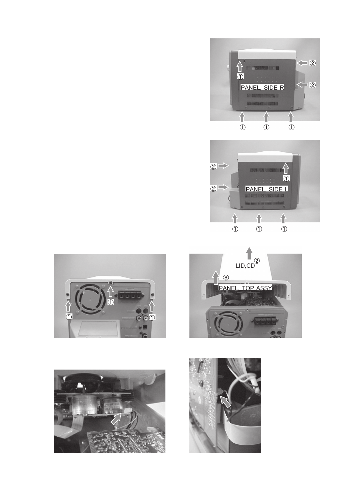
1. Removing the ornamental parts
1) Remove the six screws (four (1)s, two (2)s) and remove the
PANEL, SIDE R.
2) Remove the six screws (four (1)s, two (2)s) and remove the
PANEL, SIDE L.
3) Remove the three screws (1), open the LID, CD (2), and lift up the PANEL, TOP ASSY (3).
4) Remove the two connectors.
– 4 –
Page 5
5) Short the short land (1) of the Pick Up by soldering, pull out the FFC,
16P (2) and remove the PANEL, TOP ASSY.
6) Remove the 11 screws (1). Disconnect the connector (2) of the FAN and remove the CABI, REAR.
7) This picture indicates the status of the unit with the ornamental
parts removed.
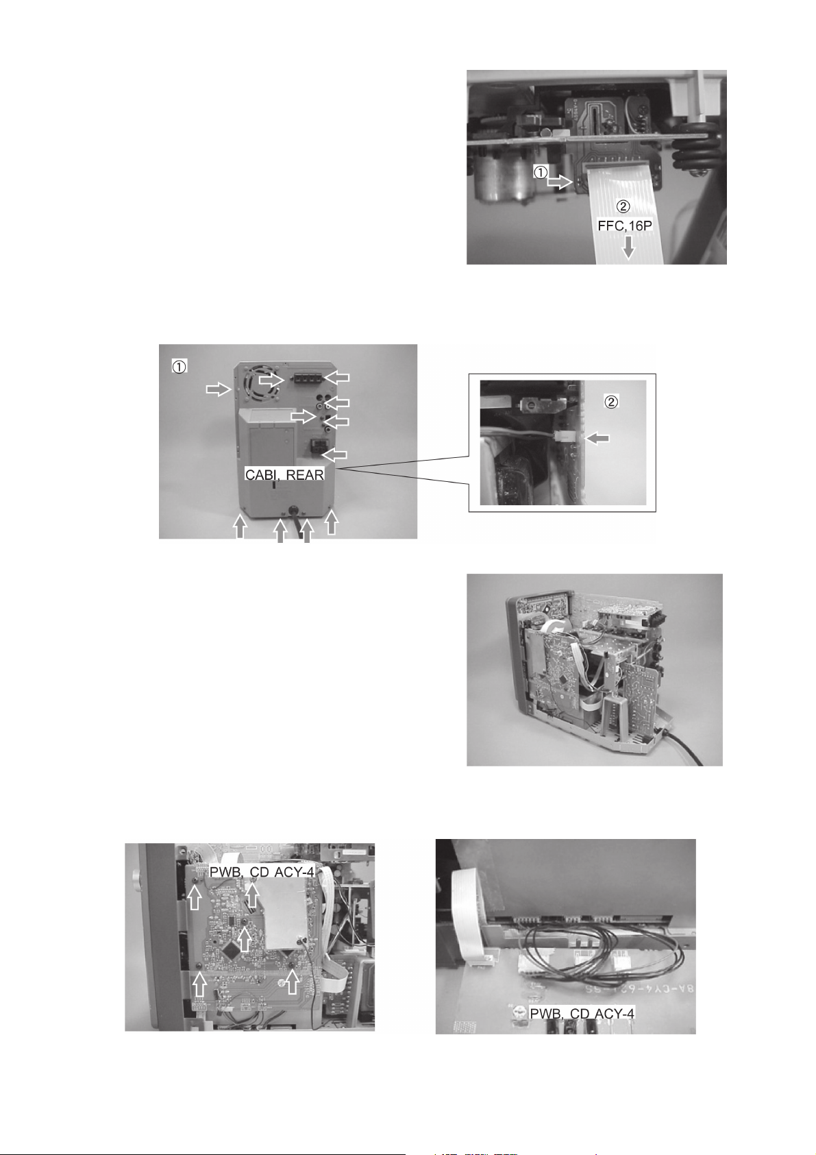
2. Removing the PWB, CD ACY-4
1) Remove the five screws, disconnect the FFC, wires, etc., and remove the PWB, CD ACY-4.
– 5 –
Page 6
3. Removing the PWB, MAIN ASSY.
1) Remove the screw (1) and remove the connector (2).
2) Remove the screw (1) and remove the PWB, MAIN ASSY in the direction of the arrow (2).
(The board is hooked. While lifting up the hook, remove the board.)
4. Removing the FRONT block.
1) Remove the two screws securing the CAB, FR ASSY.
2) Remove the two screws (1) and remove the CABI, FR ASSY in the direction of the arrow (2).
– 6 –
Page 7
3) This picture indicates the status of the unit with the PWB, MAIN
ASSY and CABI, FRONT ASSY removed.
5. Removing the CD-R/RW drive unit (CRD-RA1).
1) Remove the four screws and remove the HLDR, PWB
CD.
2) Remove the three screws and remove the PLATE,
SHILD TOP.
3) Rotate the gear (1) in the direction of the arrow and open the tray (2). Remove the four screws (3) and remove the CD-R/RW
drive unit.
– 7 –
Page 8
Notes during re-assembling
When assemble the magical change panel, adjust the phase of the gear.
1. Phase adjustment of the GEAR, OPE 1 and GEAR, WORM WHEEL.
1) Align holes 1.
2) Then, move the position of the holes of each gear as shown by 2 in the illustration.
2. Installation Procedure of HLDR, GEAR ASSY
1) Position the panel side so that it faces front as shown in the illustration.
2) Install the HLDR, GEAR ASSY.
8
Page 9

ELECTRICAL MAIN PARTS LIST
PART NO. DESCRIPTIONREF. NO. KANRI
NO.
IC
87-A20-446-010 C-IC,LA9241ML
87-A20-459-010 C-IC,LC78622ED
87-017-917-080 IC,BU4066BCF
87-A21-093-010 IC,LA6541D
87-A21-715-010 IC,PQ15RW21
87-A21-021-040 C-IC,BU2099FV
8A-CY4-602-010 C-IC,LC876564V-5S65:ACY-4
87-A21-573-010 IC,SPS-448-1-E
87-A21-452-030 C-IC,BD3876KS2
87-A21-103-040 C-IC,MM1454XFBE
87-070-289-040 IC,BU2092F
87-001-755-080 IC,NJM78L05UA
87-070-127-110 IC,LC72131D
87-A20-913-010 IC,LA1837NL
87-A20-870-010 IC,GP1F37R
TRANSISTOR
87-A30-073-080 C-TR,RT1N 141C
87-026-463-080 TR,2SA933S (0.3W)
87-A30-076-080 C-TR,2SC3052F
87-026-239-080 C-TR,DTC114TK (0.2W)
87-A30-427-040 C-TR,DTC114EKA
89-213-702-010 TR,2SB1370 (1.8W)
87-026-610-080 TR,KTC3198GR
87-A30-075-080 C-TR,2SA1235F
87-A30-234-080 TR,CSC4115BC
87-026-580-080 C-TR,DTA123JK
87-A30-107-070 C-TR,CMBT5401
87-A30-087-080 C-FET,2SK2158
87-A30-074-080 C-TR,RT1P 141C
87-026-609-080 TR,KTA1266GR
87-A30-190-080 TR,CC5551
87-A30-106-070 C-TR,CMBT5551
87-A30-105-080 C-TR,RT1P 441C
87-A30-137-010 TR,2SD2494
87-A30-138-010 TR,2SB1625
87-A30-257-080 C-TR,2SD1306E
87-A30-240-080 TR,CSA1585BC
87-A30-047-080 TR,CSD655E
87-026-235-080 CHIP-TR,DTC114EK
87-026-297-080 C-TR,DTA144TK
89-113-184-080 TR,2SA1318T
89-113-695-680 C-TR,2SA1369G/H
87-A30-071-080 C-TR,RT1N 144C
87-026-233-080 C-TR,DTA114TK
87-A30-072-080 C-TR,RT1P 144C
89-327-143-080 C-TR,2SC2714(0.1W)
DIODE
87-020-465-080 DIODE,1SS133 (110MA)
87-A40-270-080 C-DIODE,MC2838
87-A40-269-080 C-DIODE,MC2836
87-070-274-080 DIODE,1N4003 SEM
87-070-022-010 DIODE,IN5402 (RECT)
87-A40-345-080 ZENER,MTZJ10C
87-A40-004-080 ZENER,MTZJ16A
87-070-322-080 ZENER,MTZJ 36D
87-A40-341-080 ZENER,MTZJ 36 A
87-A40-250-040 C-DIODE,DAN217
87-A40-488-080 DIODE,1SS244
87-A40-437-080 ZENER,MTZJ4.3B
87-A40-002-080 ZENER,MTZJ5.1C
87-017-932-080 ZENER,MTJ6.2B
87-070-136-080 ZENER,MTZJ5.1B
87-017-099-080 ZENER,HZS6B3
87-017-121-080 ZENER,HZS11A1
87-A40-871-080 ZENER,MTZJ5.6PC
DESCRIPTIONREF. NO. KANRI
PART NO.
NO.
87-017-149-080 ZENER,HZS6A2L
MAIN C.B
C104 87-012-368-080 C-CAP,S 0.1-50 F
C105 87-012-368-080 C-CAP,S 0.1-50 F
C106 87-010-196-080 CHIP CAPACITOR,0.1-25
C107 87-010-196-080 CHIP CAPACITOR,0.1-25
C108 87-010-196-080 CHIP CAPACITOR,0.1-25
C109 87-010-196-080 CHIP CAPACITOR,0.1-25
C110 87-010-928-000 CAP,E 4700-25 M SMG
C111 87-010-197-080 CAP,CHIP 0.01 DM
C113 87-010-408-080 CAP,ELECT 47-50V
C114 87-010-112-080 CAP,ELECT 100-16V
C115 87-010-235-080 CAP,E 470-16 SME
C116 87-012-368-080 C-CAP,S 0.1-50 F
C117 87-012-368-080 C-CAP,S 0.1-50 F
C118 87-016-658-000 CAP,E 4700-35 M SMG
C119 87-016-658-000 CAP,E 4700-35 M SMG
C131 87-010-263-080 CAP,ELECT 100-10V
C132 87-010-405-080 CAP,ELECT 10-50V
C133 87-010-194-080 CAP,CHIP 0.047
C134 87-010-194-080 CAP,CHIP 0.047
C152 87-010-496-040 CAP,ELECT 3.3-50 M 5L
C161 87-010-260-080 CAP,ELECT 47-25V
C163 87-010-197-080 CAP,CHIP 0.01 DM
C166 87-010-196-080 CHIP CAPACITOR,0.1-25
C167 87-010-196-080 CHIP CAPACITOR,0.1-25
C171 87-010-260-080 CAP,ELECT 47-25V
C172 87-010-260-080 CAP,ELECT 47-25V
C173 87-010-260-080 CAP,ELECT 47-25V
C174 87-010-260-080 CAP,ELECT 47-25V
C175 87-A10-944-080 CAP,ELECT 100-100V
C176 87-010-263-080 CAP,ELECT 100-10V
C181 87-010-196-080 CHIP CAPACITOR,0.1-25
C182 87-A11-233-090 CAP,E 4700-16 105 KMG
C183 87-010-196-080 CHIP CAPACITOR,0.1-25
C186 87-016-080-090 CAP,E 3300-16 M SME
C191 87-010-196-080 CHIP CAPACITOR,0.1-25
C192 87-010-196-080 CHIP CAPACITOR,0.1-25
C193 87-010-196-080 CHIP CAPACITOR,0.1-25
C194 87-010-196-080 CHIP CAPACITOR,0.1-25
C201 87-010-260-080 CAP,ELECT 47-25V
C202 87-010-260-080 CAP,ELECT 47-25V
C203 87-A10-946-080 C-CAP,S 220P-100 J CH
C204 87-A10-946-080 C-CAP,S 220P-100 J CH
C209 87-010-178-080 CHIP CAP,1000P
C210 87-010-178-080 CHIP CAP,1000P
C211 87-012-368-080 C-CAP,S 0.1-50 F
C212 87-012-368-080 C-CAP,S 0.1-50 F
C213 87-010-195-080 C-CAP,S 0.068-25 F
C214 87-010-195-080 C-CAP,S 0.068-25 F
C215 87-012-368-080 C-CAP,S 0.1-50 F
C216 87-012-368-080 C-CAP,S 0.1-50 F
C217 87-010-182-080 C-CAP,S 2200P-50 B
C218 87-010-182-080 C-CAP,S 2200P-50 B
C219 87-012-368-080 C-CAP,S 0.1-50 F
C220 87-012-368-080 C-CAP,S 0.1-50 F
C221 87-010-186-080 CAP,CHIP 4700P
C222 87-010-186-080 CAP,CHIP 4700P
C223 87-010-401-080 CAP,ELECT 1-50V
C254 87-010-494-040 CAP,ELECT 1-50V M5L
C256 87-010-492-040 CAP,ELECT 0.33-50 M5L
C261 87-010-197-080 CAP,CHIP 0.01 DM
C262 87-010-197-080 CAP,CHIP 0.01 DM
C265 87-010-546-080 CAP,ELECT 0.33-50V
C266 87-010-546-080 CAP,ELECT 0.33-50V
C267 87-010-260-080 CAP,ELECT 47-25V
C277 87-010-197-080 CAP,CHIP 0.01 DM
– 9 –
Page 10

PART NO. DESCRIPTIONREF. NO. KANRI
NO.
C283 87-010-184-080 C-CAP,S 3300P-50 KB
C284 87-010-184-080 C-CAP,S 3300P-50 KB
C401 87-010-494-080 CAP,ELECT 1-50V
C491 87-010-496-080 CAP,ELECT 3.3-50 M5L
C492 87-010-496-080 CAP,ELECT 3.3-50 M5L
C402 87-010-263-080 CAP,E 100-10 M 11L SME
C403 87-010-260-080 CAP,E 47-25 M 11L SME
C410 87-010-260-080 CAP,E 47-25 M 11L SME
C461 87-010-402-080 CAP,ELECT 2.2-50V
C462 87-010-400-080 CAP,ELECT 0.47-50V
C501 87-010-374-080 CAP,ELECT 47-10V
C502 87-010-374-080 CAP,ELECT 47-10V
C515 87-010-318-080 C-CAP,S 47P-50 CH
C516 87-010-318-080 C-CAP,S 47P-50 CH
C517 87-010-318-080 C-CAP,S 47P-50 CH
C518 87-010-318-080 C-CAP,S 47P-50 CH
C521 87-010-956-080 CHIP-CAP,S 0.068-25B
C522 87-016-369-080 C-CAP,S 0.033-25 B K
C524 87-010-401-080 CAP,ELECT 1-50V
C525 87-016-081-080 C-CAP,S 0.1-16 RK
C526 87-016-081-080 C-CAP,S 0.1-16 RK
C527 87-010-197-080 CAP,CHIP 0.01 DM
C531 87-010-404-080 CAP,ELECT 4.7-50V
C532 87-010-404-080 CAP,ELECT 4.7-50V
C535 87-A11-590-080 C-CAP,S 0.047-16 KB
C536 87-A11-590-080 C-CAP,S 0.047-16 KB
C537 87-010-400-080 CAP,ELECT 0.47-50V
C538 87-010-400-080 CAP,ELECT 0.47-50V
C539 87-010-185-080 C-CAP,S 3900P-50 KB
C540 87-010-185-080 C-CAP,S 3900P-50 KB
C541 87-A10-307-080 CAP,M 0.1-50 J
C542 87-A10-307-080 CAP,M 0.1-50 J
C543 87-A10-307-080 CAP,M 0.1-50 J
C544 87-A10-307-080 CAP,M 0.1-50 J
C545 87-016-081-080 C-CAP,S 0.1-16 RK
C546 87-016-081-080 C-CAP,S 0.1-16 RK
C547 87-010-401-080 CAP,ELECT 1-50V
C548 87-010-196-080 CHIP CAPACITOR,0.1-25
C549 87-010-401-080 CAP,ELECT 1-50V
C550 87-010-401-080 CAP,ELECT 1-50V
C551 87-010-402-080 CAP,ELECT 2.2-50V
C552 87-010-402-080 CAP,ELECT 2.2-50V
C561 87-010-407-080 CAP,ELECT 33-50V
C562 87-010-407-080 CAP,ELECT 33-50V
C563 87-012-158-080 C-CAP,S 390P-50 CH
C564 87-A12-001-080 CAP,E 2200-10 M SME
C565 87-010-403-080 CAP,E 3.3-50 M 11L SME
C581 87-010-404-080 CAP,ELECT 4.7-50V
C582 87-010-404-080 CAP,ELECT 4.7-50V
C595 87-010-493-080 CAP,ELECT 0.47-50V
C603 87-010-544-080 CAP,ELECT 0.1-50V
C604 87-010-544-080 CAP,ELECT 0.1-50V
C605 87-010-408-080 CAP,ELECT 47-50V
C607 87-010-405-080 CAP,ELECT 10-50V
C608 87-010-405-080 CAP,ELECT 10-50V
C609 87-010-196-080 CHIP CAPACITOR,0.1-25
C610 87-010-384-080 CAP,ELECT 100-25V
C611 87-010-197-080 CAP,CHIP 0.01 DM
C612 87-010-197-080 CAP,CHIP 0.01 DM
C901 87-010-196-080 CHIP CAPACITOR,0.1-25
C902 87-010-178-080 CHIP CAP,1000P
C903 87-010-178-080 CHIP CAP,1000P
CN401 87-A60-619-010 CONN,2P V 2MM JMT
CN501 87-099-719-010 CONN,30P TYK-B(X)
CN502 87-A60-423-010 CONN,14P V TOC-B
CN503 87-A60-133-010 CONN,8P V FE
CN571 87-099-570-010 CONN,13P TUC-P13P-B1
CNA101 8A-CJ4-640-010 CONN ASSY,3P V AC1
CNA901 8Z-CL4-656-010 CONN ASSY,2P V DTL SHLD
FC502 8A-CY4-638-010 FF-CABLE,14P 1.0 200MM
DESCRIPTIONREF. NO. KANRI
PART NO.
NO.
FC503 88-908-301-210 FF-CABLE,8P 1.25
H101 87-A90-511-010 HLDR,WIRE 2.5 10P
J201 87-A60-420-010 JACK,3.5 ST(MSC)
J202 87-099-801-010 JACK,PIN 1P BLK
J203 87-A60-238-010 TERMINAL,SP 4P(MSC)
J501 87-A60-354-010 JACK,PIN 2P MSP -242V-05
L201 87-003-383-010 COIL,1UH-S
L202 87-003-383-010 COIL,1UH-S
L203 87-003-098-080 COIL,2.2UH K LAL02
L205 87-003-098-080 COIL,2.2UH K LAL02
L206 87-003-098-080 COIL,2.2UH K LAL02
L563 87-A50-517-080 COIL,10UH K FLR88
L590 87-008-372-080 FILTER,EMIBL01RN1
R215 87-A00-258-080 RES,M/F 0.22-1W J
R216 87-A00-258-080 RES,M/F 0.22-1W J
R217 87-A00-258-080 RES,M/F 0.22-1W J
R218 87-A00-258-080 RES,M/F 0.22-1W J
R219 87-A00-258-080 RES,M/F 0.22-1W J
R220 87-A00-258-080 RES,M/F 0.22-1W J
R563 87-012-156-080 C-CAP,S 220P-50
R564 87-012-156-080 C-CAP,S 220P-50
R591 87-003-143-080 COIL,4.7UH K LAL02
R592 87-003-143-080 COIL,4.7UH K LAL02
TH251 87-A91-042-080 C-THMS,100K 55001
TH252 87-A91-042-080 C-THMS,100K 55001
W101 8Z-CL4-658-010 F-CABLE,10P 2.5 300MM
FRONT C.B
C151 87-018-209-080 CAP, CER 0.1-50V
C161 87-010-196-080 CHIP CAPACITOR,0.1-25
C162 87-010-322-080 C-CAP,S 100P-50 CH
C201 87-010-316-080 C-CAP,S 33P-50 CH
C203 87-010-313-080 CAP, CHIP 18P
C204 87-010-196-080 CHIP CAPACITOR,0.1-25
C205 87-010-196-080 CHIP CAPACITOR,0.1-25
C206 87-010-196-080 CHIP CAPACITOR,0.1-25
C207 87-010-196-080 CHIP CAPACITOR,0.1-25
C231 87-010-560-040 CAP,E 10-50 GAS
C232 87-010-178-080 CHIP CAP 1000P
C241 87-016-526-080 C-CAP,S 0.47-16 BK
C242 8A-CJ4-635-010 CAP,E 470-10 SRG3.5PITCH
C243 87-010-196-080 CHIP CAPACITOR,0.1-25
C246 87-012-393-080 C-CAP,S 0.22-16 R K
C250 87-010-198-080 CHIP CAPACITOR, 0.022-25 KB
C351 87-010-197-080 CAP, CHIP 0.01 DM
C352 87-010-197-080 CAP, CHIP 0.01 DM
C353 87-010-197-080 CAP, CHIP 0.01 DM
C354 87-010-197-080 CAP, CHIP 0.01 DM
C371 87-010-552-040 CAP,E 22-16 GAS
C372 87-010-552-040 CAP,E 22-16 GAS
C373 87-A12-078-040 CAP,E 47-35 SMG
C701 87-012-156-080 C-CAP,S 220P-50 CH
C713 87-012-156-080 C-CAP,S 220P-50 CH
CN101 87-099-720-010 CONN,30P TYK-B(P)
CN102 87-A60-984-010 CONN,17P V TOC-B
CN302 87-A60-624-010 CONN,7P V 2MM JMT
CNA303 8A-CJ4-641-110 CONN ASSY,8P H SW
D151 87-A40-317-080 LED,SLR-342VCT31 RED
D153 87-A40-317-080 LED,SLR-342VCT31 RED
D154 87-A40-317-080 LED,SLR-342VCT31 RED
D155 87-A40-317-080 LED,SLR-342VCT31 RED
D156 87-A40-317-080 LED,SLR-342VCT31 RED
D161 87-A40-786-080 LED,SMLS1BE16WTP4 BLU/UMB
D162 87-A40-786-080 LED,SMLS1BE16WTP4 BLU/UMB
D163 87-A40-786-080 LED,SMLS1BE16WTP4 BLU/UMB
FL301 8A-CY4-604-010 FL,13-ST-46GNK ACY-4
L201 87-A50-333-010 COIL,OSC 9.43MHZ
S301 87-A90-095-080 SW,TACT EVQ11G04M
– 10 –
Page 11

PART NO. DESCRIPTIONREF. NO. KANRI
NO.
S303 87-A90-095-080 SW,TACT EVQ11G04M
S304 87-A90-095-080 SW,TACT EVQ11G04M
S305 87-A90-095-080 SW,TACT EVQ11G04M
S306 87-A90-095-080 SW,TACT EVQ11G04M
S307 87-A90-095-080 SW,TACT EVQ11G04M
S309 87-A90-095-080 SW,TACT EVQ11G04M
S310 87-A90-095-080 SW,TACT EVQ11G04M
S311 87-A90-095-080 SW,TACT EVQ11G04M
S312 87-A90-095-080 SW,TACT EVQ11G04M
S352 87-A91-687-010 SW,RTRY RE012102PV-VOL
S801 87-A90-095-080 SW,TACT EVQ11G04M
S802 87-A90-095-080 SW,TACT EVQ11G04M
S803 87-A90-095-080 SW,TACT EVQ11G04M
S804 87-A90-095-080 SW,TACT EVQ11G04M
S805 87-A90-095-080 SW,TACT EVQ11G04M
S806 87-A90-095-080 SW,TACT EVQ11G04M
S807 87-A90-095-080 SW,TACT EVQ11G04M
S808 87-A90-095-080 SW,TACT EVQ11G04M
S809 87-A90-095-080 SW,TACT EVQ11G04M
S810 87-A90-095-080 SW,TACT EVQ11G04M
SW351 87-A91-753-010 SW,RTRY EC12E12504-JOG
X201 87-XMN-602-010 VIB,PIEZO PKM13EPY
CD C.B
C1 87-010-418-040 CAP, ELECT 3.3-25 M
C2 87-010-197-080 CAP, CHIP 0.01 DM
C3 87-010-263-080 CAP,E 100-10 11L
C4 87-A11-242-040 CAP, ELECT 220-10M
C5 87-010-197-080 CAP, CHIP 0.01 DM
C6 87-010-234-040 CAP,E 47-16 M 5L SRE
C7 87-012-349-080 C-CAP,S 1000P-50 CH
C8 87-010-198-080 CAP, CHIP 0.022
C9 87-A11-242-040 CAP, ELECT 220-10M 5L
C10 87-010-263-080 CAP,E 100-10 11L
C11 87-016-083-080 C-CAP,S 0.15-16 K R
C12 87-010-071-040 CAP, ELECT 1-50 M 5L SRE
C13 87-A11-586-080 C-CAP,S 0.033-50 K B
C14 87-010-405-080 CAP ELECT 10-50 M 11L
C15 87-010-196-080 CHIP CAPACITOR,0.1-25
C16 87-015-962-040 CAP ELECT 0.22-50 M 5L
C17 87-012-157-080 C-CAP,S 330P-50 CH
C18 87-010-213-080 C-CAP,S 0.015-50 B
C19 87-A10-201-080 C-CAP,S0.33-16 KB
C20 87-A11-586-080 C-CAP,S 0.033-50 K B
C21 87-A12-308-080 C-CAP,S 0.15-25 K B
C22 87-010-184-080 C-CAP,S 3300P-50 K B
C23 87-A11-591-080 C-CAP,S 0.047-25 K B
C24 87-A11-606-080 C-CAP,S 0.047-25 K B
C25 87-010-994-080 C-CAP,S 680P-50 CH
C26 87-A10-201-080 C-CAP,S0.33-16 KB
C28 87-010-197-080 CAP, CHIP 0.01 DM
C29 87-010-186-080 CAP,CHIP 4700P
C30 87-012-156-080 C-CAP,S 220P-50 CH
C31 87-015-962-040 CAP ELECT 0.22-50 M 5L
C32 87-015-680-040 CAP,E 47-10 M 7L SRE
C33 87-010-071-040 CAP, ELECT 1-50 M 5L SRE
C34 87-010-184-080 CHIP CAPACITOR 3300P(K)
C35 87-010-197-080 CAP, CHIP 0.01 DM
C36 87-010-374-080 CAP,E 47-10 M11L SME
C37 87-010-404-080 CAP, ELECT 4.7-50V
C38 87-010-196-080 CHIP CAPACITOR,0.1-25
C39 87-012-349-080 C-CAP,S 1000P-50 CH
C40 87-010-145-080 C-CAP,S 1P-50 C CH GRM
C41 87-010-184-080 CHIP CAPACITOR 3300P(K)
C42 87-010-313-080 C-CAP,S 18P-50 CH
C45 87-010-196-080 CHIP CAPACITOR,0.1-25
C46 87-010-196-080 CHIP CAPACITOR,0.1-25
C47 87-010-196-080 CHIP CAPACITOR,0.1-25
C48 87-010-315-080 C-CAP,S 27P-50 CH
DESCRIPTIONREF. NO. KANRI
PART NO.
NO.
C50 87-015-968-040 CAP,E 4.7-16 M 5L SRE
C51 87-012-156-080 C-CAP,S 220P-50 CH
C53 87-010-322-080 C-CAP,S 100P-50 CH
C55 87-010-263-080 CAP,E 100-10 11L
C57 87-010-316-080 C-CAP,S 33P-50 CH
C58 87-010-316-080 C-CAP,S 33P-50 CH
C59 87-010-263-080 CAP,E 100-10 11L
C60 87-010-196-080 CHIP CAPACITOR,0.1-25
C61 87-010-196-080 CHIP CAPACITOR,0.1-25
C62 87-010-371-080 CAP, ELECT 470-6.3V
C65 87-010-404-080 CAP, ELECT 4.7-50V
C66 87-010-196-080 CHIP CAPACITOR,0.1-25
C67 87-010-263-080 CAP,E 100-10 11L
C68 87-010-322-080 C-CAP,S 100P-50 CH
C69 87-012-154-080 C-CAP,S 150P-50 CH
C70 87-012-156-080 C-CAP,S 220P-50 CH
C72 87-012-140-080 C-CAP,S 470P-50 J CH
C81 87-010-417-080 CAP,E 2.2-35 5L
C82 87-010-417-080 CAP,E 2.2-35 5L
C83 87-010-181-080 CAP,CHIP S 1800P
C84 87-010-181-080 CAP,CHIP S 1800P
C90 87-010-196-080 CHIP CAPACITOR,0.1-25
C93 87-010-196-080 CAP, CHIP 0.1-25 Z F
C94 87-010-197-080 CAP, CHIP 0.01 DM
C95 87-010-197-080 CAP, CHIP 0.01 DM
C101 87-010-322-080 C-CAP,S 100P-50 CH
C102 87-010-322-080 C-CAP,S 100P-50 CH
C103 87-010-322-080 C-CAP,S 100P-50 CH
C104 87-010-322-080 C-CAP,S 100P-50 CH
C105 87-010-322-080 C-CAP,S 100P-50 CH
C106 87-012-350-080 C-CAP,S 1-25 Z F
C110 87-010-196-080 CHIP CAPACITOR,0.1-25
C495 87-010-196-080 CHIP CAPACITOR,0.1-25
C601 87-010-263-080 CAP,E 100-10 11L
C620 87-010-196-080 CHIP CAPACITOR,0.1-25
C660 87-010-197-080 CAP, CHIP 0.01 DM
C661 87-010-197-080 CAP, CHIP 0.01 DM
C671 87-010-196-080 CHIP CAPACITOR,0.1-25
C672 87-010-196-080 CHIP CAPACITOR,0.1-25
C673 87-010-196-080 CHIP CAPACITOR,0.1-25
C674 87-010-196-080 CHIP CAPACITOR,0.1-25
C675 87-010-197-080 CAP, CHIP 0.01 DM
C676 87-A12-326-080 CAP,E 1000-16 RS
C679 87-010-263-080 CAP,E 100-10 11L
C680 87-010-197-080 CAP, CHIP 0.01 DM
C901 87-A11-727-080 C-CAP,S 0.33-25 Z F
C902 87-010-196-080 CHIP CAPACITOR,0.1-25
C905 87-012-156-080 CAP 220P-50 J CH
C906 87-012-156-080 CAP 220P-50 J CH
C907 87-012-156-080 CAP 220P-50 J CH
C908 87-012-156-080 CAP 220P-50 J CH
C909 87-012-156-080 CAP 220P-50 J CH
C910 87-012-156-080 CAP 220P-50 J CH
C911 87-012-156-080 CAP 220P-50 J CH
C912 87-010-263-080 CAP,E 100-10 11L
C913 87-010-197-080 CAP, CHIP 0.01 DM
C916 87-012-156-080 CAP 220P-50 J CH
C917 87-012-156-080 CAP 220P-50 J CH
C918 87-012-156-080 CAP 220P-50 J CH
CN1 87-A60-424-010 CONN,16P V TOC-B
CN2 87-009-034-010 CONN,6P PH V
CN3 87-009-345-010 CONN,2P H WHT PH
CN4 87-A61-283-010 CONN,17P V FWN-BTRK
CN5 87-A60-156-010 CONN,8P H FE
CN6 87-A61-375-010 CONN,9P H GRY FMN-SSTK
CN7 87-A61-089-010 CONN,14P H GRY FMN-SSTK
CN8 87-009-349-010 CONN,6P PH H
CN9 87-009-347-010 CONN,4P PH H WHT
CN10 87-009-346-010 CONN,3P PH H
CN11 87-A60-619-010 CONN,2P V 2MM JMT
– 11 –
Page 12

PART NO. DESCRIPTIONREF. NO. KANRI
CNA12 88-805-042-490 CONN ASSY,4P
NO.
DESCRIPTIONREF. NO. KANRI
FC1 8A-CY4-631-010 FF-CABLE,16P 1.0 220MM
FC4 8A-CJ4-645-010 FF-CABLE,17P 1.0
FC6 8A-CY4-637-010 FF-CABLE,9P 1.25 100MM
JR907 83-XM1-617-080 C-COIL,BK2125HM601
JR908 83-XM1-617-080 C-COIL,BK2125HM601
JR909 83-XM1-617-080 C-COIL,BK2125HM601
JR910 83-XM1-617-080 C-COIL,BK2125HM601
JR911 87-A50-189-080 C-COIL,S BLM21B272S
JR912 83-XM1-617-080 C-COIL,BK2125HM601
JR913 87-A50-189-080 C-COIL,S BLM21B272S
JR914 87-A50-190-080 C-COIL,S BLM21A102S
JR915 87-A50-190-080 C-COIL,S BLM21A102S
JR916 87-A50-190-080 C-COIL,S BLM21A102S
JR917 87-A50-190-080 C-COIL,S BLM21A102S
JR918 87-A50-190-080 C-COIL,S BLM21A102S
JR919 87-A50-190-080 C-COIL,S BLM21A102S
JR920 87-A50-190-080 C-COIL,S BLM21A102S
JR922 83-XM1-617-080 C-COIL,BK2125HM601
JW39 87-008-372-080 FLTR,EMI BL01 RN1
L1 87-003-102-080 COIL, 10UH
L2 87-003-146-080 COIL,15UH LAL02
L3 87-008-372-080 FILTER, EMI BL OIRNI
L4 87-003-102-080 COIL, 10UH
L5 87-003-152-080 COIL, 100UH
L6 87-003-102-080 COIL, 10UH
L7 87-003-102-080 COIL, 10UH
L8 87-003-102-080 COIL, 10UH
R68 87-A50-189-080 C-COIL,S BLM21B272S
R133 87-A50-190-080 C-COIL,S BLM21A102S
SFR130 87-024-437-080 SFR100K,RH063EC
X1 87-A70-046-010 VIB,XTAL 16.934MHZ
FACE-A C.B
C824 87-010-197-080 CAP, CHIP 0.01 DM
CNA801 8A-CJ4-650-010 CONN ASSY,2P V FACE A
FACE-B C.B
C152 87-010-196-080 CHIP CAPACITOR,0.1-25
C801 87-010-322-080 C-CAP,S 100P-50 CH
C802 87-010-322-080 C-CAP,S 100P-50 CH
C821 87-010-196-080 CHIP CAPACITOR,0.1-25
C826 87-010-197-080 CAP, CHIP 0.01 DM
C827 87-010-197-080 CAP, CHIP 0.01 DM
C829 87-010-197-080 CAP, CHIP 0.01 DM
C830 87-010-197-080 CAP, CHIP 0.01 DM
CN801 87-A60-619-010 CONN,2P V 2MM JMT
CNA302 8A-CL4-641-010 CONN ASSY,7P H PANEL
CNA804 8A-CL4-644-010 CONN ASSY,3P V FACE C
D831 87-A40-496-040 LED,SLR-342MCT31 GRN
D832 87-A40-496-040 LED,SLR-342MCT31 GRN
D833 87-A40-496-040 LED,SLR-342MCT31 GRN
D834 87-A40-496-040 LED,SLR-342MCT31 GRN
D835 87-A40-496-040 LED,SLR-342MCT31 GRN
L151 87-003-154-080 COIL, 220UH J LALO2
L152 87-003-154-080 COIL, 220UH J LALO2
FACE-C C.B
C825 87-010-197-080 CAP, CHIP 0.01 DM
CN804 87-A60-620-010 CONN,3P V 2MM JMT
S861 87-A90-095-080 SW,TACT EVQ11G04M
S862 87-A90-095-080 SW,TACT EVQ11G04M
S863 87-A90-095-080 SW,TACT EVQ11G04M
S864 87-A90-095-080 SW,TACT EVQ11G04M
S865 87-A90-095-080 SW,TACT EVQ11G04M
S866 87-A90-095-080 SW,TACT EVQ11G04M
PART NO.
SW-1 C.B
NO.
C901 87-010-264-040 CAP,E 100-10 5L
C902 87-010-264-040 CAP,E 100-10 5L
CN303 87-A60-672-010 CONN,8P H 2MM JMT
CNA901 8A-CJ4-646-010 CONN ASSY,2P V SW-2
S902 87-A90-117-010 SW,PUSH 1-1-1 MPU103
S903 87-A90-117-010 SW,PUSH 1-1-1 MPU103
S904 87-A90-117-010 SW,PUSH 1-1-1 MPU103
SW-2 C.B
S901 87-A90-117-010 SW,PUSH 1-1-1 MPU103
PT1 C.B
C1 87-010-387-080 CAP,E 470-25 M SME
C3 87-A10-479-080 CAP,CER 2200P-250 M E KH
!
C4 87-A10-479-080 CAP,CER 2200P-250 M E KH
!
C5 87-010-403-080 CAP,ELECT 3.3-50V
CN1 87-A60-620-010 CONN,3P V 2MM JMT
!
PT2 8Z-NF8-663-010 PT,SUB ZNF-8(H)
!
RY2 87-A91-339-010 RELAY,AC DC12V G5PA-2
!
T1 87-A60-317-010 TERMINAL,1P MSC
!
T2 87-A60-317-010 TERMINAL,1P MSC
S1 87-A90-234-010 SW,SL 1-2-2 SWS2201
!
PT2 C.B
H51 87-A90-511-010 HLDR,WIRE 2.5 10P
PR51 87-A90-094-080 PROTECTOR,4A 491SERIES 60V
!
PR52 87-A90-094-080 PROTECTOR,4A 491SERIES 60V
!
PR53 87-026-681-080 PROTECTOR,5A 491SERIES 60V
!
PR54 87-026-681-080 PROTECTOR,5A 491SERIES 60V
!
PR55 87-026-681-080 PROTECTOR,5A 491SERIES 60V
!
PR56 87-026-681-080 PROTECTOR,5A 491SERIES 60V
!
!
PT1 8A-CJ4-606-010 PT,H ACJ-4
MOTOR C.B
M1 S0-M10-A09-700 MOTOR SLED ASSY
PIN3 S2-369-750-000 PLUG,6P
SW1 S4-S13-A01-600 SW,LEAF
REG C.B
C91 87-010-112-080 CAP,E 100-16
C92 87-A11-727-080 C-CAP,S 0.33-25 Z F
CN12 87-009-032-010 CONN,4P YEL
TUNER C.B
C701 87-010-381-080 CAP,ELECT 330-16V
C702 87-010-404-080 CAP,ELECT 4.7-50V
C703 87-012-286-080 CAP,U 0.01-25
C704 87-012-286-080 CAP,U 0.01-25
C705 87-A10-592-080 C-CAP,S 0.015-50 J B
C706 87-A10-592-080 C-CAP,S 0.015-50 J B
C709 87-012-195-080 C-CAP,U 100P-50CH
C711 87-010-260-080 CAP,ELECT 47-25V
C712 87-010-831-080 C-CAP,U,0.1-16F
C714 87-012-286-080 CAP,U 0.01-25
C717 87-012-286-080 CAP,U 0.01-25
C719 87-012-286-080 CAP,U 0.01-25
C720 87-012-195-080 C-CAP,U 100P-50CH
C721 87-012-176-080 CAP,15P
C722 87-012-176-080 CAP,15P
C723 87-012-274-080 CHIP CAP,U 1000P-50B
C725 87-012-274-080 CHIP CAP,U 1000P-50B
C727 87-010-196-080 CHIP CAPACITOR,0.1-25
C728 87-010-248-080 CAP,ELECT 220-10V
– 12 –
Page 13
PART NO. DESCRIPTIONREF. NO. KANRI
NO.
C729 87-012-274-080 CHIP CAP,U 1000P-50B
C731 87-012-286-080 CAP,U 0.01-25
C733 87-010-987-080 C-CAP,S 1500P-50 CH
C734 87-010-987-080 C-CAP,S 1500P-50 CH
C735 87-010-987-080 C-CAP,S 1500P-50 CH
C736 87-010-987-080 C-CAP,S 1500P-50 CH
C737 87-A10-592-080 C-CAP,S 0.015-50 J B
C738 87-A10-592-080 C-CAP,S 0.015-50 J B
C751 87-010-220-080 C-CAP,S 0.018-25 K B
C752 87-010-220-080 C-CAP,S 0.018-25 K B
C756 87-012-286-080 CAP,U 0.01-25
C757 87-012-188-080 C-CAP,U 47P-50 CH
C758 87-012-167-080 C-CAP,U 5P-50 CH
C763 87-010-829-080 CAP,U 0.047-16
C764 87-012-337-080 C-CAP,U 56P-50 CH
C765 87-012-286-080 CAP,U 0.01-25
C768 87-012-286-080 CAP,U 0.01-25
C769 87-010-260-080 CAP,ELECT 47-25V
C770 87-010-829-080 CAP,U 0.047-16
C771 87-010-383-080 CAP,ELECT 33-25V
C772 87-010-829-080 CAP,U 0.047-16
C773 87-010-196-080 CHIP CAPACITOR,0.1-25
C774 87-010-263-080 CAP,ELECT 100-10V
C775 87-010-404-080 CAP,ELECT 4.7-50V
C776 87-012-286-080 CAP,U 0.01-25
C777 87-010-400-080 CAP, ELECT 0.47-50V
C778 87-010-401-080 CAP,ELECT 1-50V
C779 87-010-401-080 CAP,ELECT 1-50V
C780 87-010-196-080 CHIP CAPACITOR,0.1-25
C781 87-010-405-080 CAP,ELECT 10-50V
C782 87-010-405-080 CAP,ELECT 10-50V
C783 87-012-286-080 CAP,U 0.01-25
C784 87-012-286-080 CAP,U 0.01-25
C785 87-010-401-080 CAP, ELECT 1-50V
C786 87-010-401-080 CAP, ELECT 1-50V
DESCRIPTIONREF. NO. KANRI
PART NO.
NO.
C789 87-012-275-080 C-CAP,U 1200P-50 B
C790 87-012-275-080 C-CAP,U 1200P-50 B
C791 87-010-405-080 CAP,ELECT 10-50V
C793 87-012-273-080 C-CAP,U 820P-50 B
C794 87-010-406-080 CAP,ELECT 22-50
C795 87-010-596-080 CAP,S 0.047-16
C796 87-010-403-080 CAP,ELECT 3.3-50V
C799 87-010-829-080 CAP,U 0.047-16
C812 87-012-286-080 CAP,U 0.01-25
C820 87-010-260-080 CAP,ELECT 47-25V
C821 87-012-286-080 CAP,U 0.01-25
C822 87-012-286-080 CAP,U 0.01-25
C823 87-012-286-080 CAP,U 0.01-25
C828 87-010-196-080 CHIP CAPACITOR,0.1-25
C829 87-010-196-080 CHIP CAPACITOR,0.1-25
C959 87-010-196-080 CHIP CAPACITOR,0.1-25
C960 87-010-196-080 CHIP CAPACITOR,0.1-25
C961 87-012-170-080 C-CAP,U 8P-50 CH
C963 87-010-196-080 CHIP CAPACITOR,0.1-25
CF801 87-008-261-010 FILTER, SFE10.7MA5-A
CF802 87-008-261-010 FILTER, SFE10.7MA5-A
CN701 87-A60-700-010 CONN,13P H GRY TUC-P13X-C1
FFE801 A8-6ZA-19C-170 6ZA-1 YFEENC
J801 87-A60-702-010 TERMINAL,ANT 4P CJ-9036
L771 87-A50-266-010 COIL,FM DET-2N(TOK)
L772 87-A91-110-010 FLTR,PCFJZH-450 (TOK)
L981 8Z-ZA1-667-010 COIL,AM PACK 4F(TOK)
X721 87-A70-061-010 VIB,XTAL 4.500MHZ CSA-309
SW C.B
CNA103 88-805-022-010 CONN ASSY,2P BRO
S101 87-036-252-010 SW, MICRO SPPB51
CHIP RESISTOR PART CODE
Chip Resistor Part Coding
88
A
Resistor Code
Chip resistor
Wattage Type Tolerance
1/16W 1005 5% CJ
1/16W
1/10W
1/8W
1608
2125
3216
5%
5%
5%
Symbol
CJ
CJ
CJ
Figure
Value of resistor
Form
L
– 13 –
Dimensions (mm)
t
W
0.55
Resistor Code
108
118
128
LW t
1.0 0.5 0.35 104
1.6 0.8 0.45
2 1.25 0.45
3.2
1.6
: A
: A
Page 14
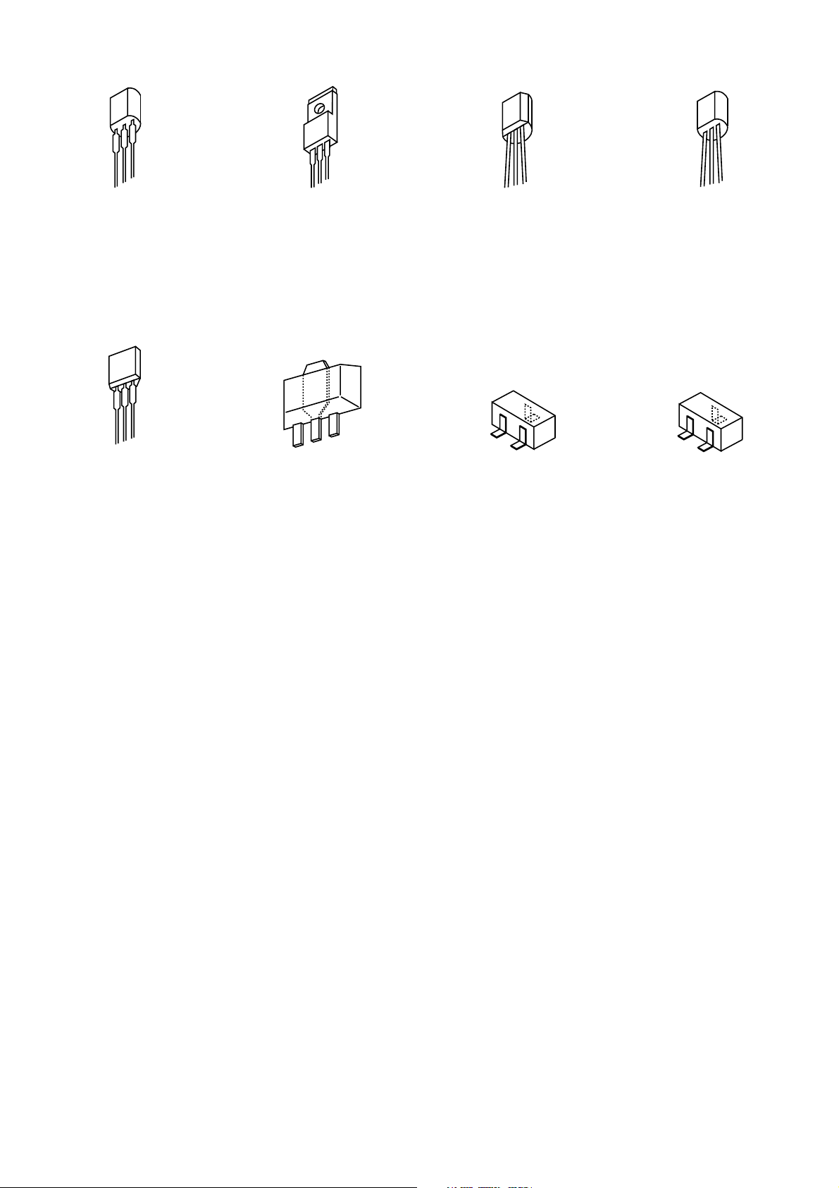
TRANSISTOR ILLUSTRATION
E C B
CC5551
CSA1585BC
CSC4115BC
KTA1266GR
KTC3198GR
E C B
2SA933S
B C E
2SB1370
2SB1625
2SD2494
CBE
2SA1369G/H
E C B
2SA1318T
G
S
2SK2158
E C B
CSD655E
D
B
2SA1235F
2SC2714
2SC3052F
2SD1306E
CMBT5401
CMBT5551
DTA123JK
DTA144TK
C
E
DTC114EK
DTC114EKA
DTC114TK
RT1N141C
RT1N144C
RT1P141C
RT1P144C
RT1P441C
DTA114TK
– 14 –
Page 15

WIRING – 1 (MAIN)
32 31 30 29 28 27 26 25 24 23 22 21 20 19 18 17 16 15 14 13 12 11 10 9 8 7 6 5 4 3 2 1
A
B
C
D
E
F
G
H
I
J
K
L
M
N
O
P
Q
– 15 –
R
S
T
U
Page 16

SCHEMATIC DIAGRAM – 1 (MAIN / PT1 / PT2)
– 16 –
Page 17

WIRING – 2 (FRONT / SW – 1 / SW – 2)
32 31 30 29 28 27 26 25 24 23 22 21 20 19 18 17 16 15 14 13 12 11 10 9 8 7 6 5 4 3 2 1
A
B
C
D
E
F
G
H
I
J
K
L
M
N
O
P
Q
– 17 –
R
S
T
U
Page 18

SCHEMATIC DIAGRAM – 2 (FRONT / FACE–A / FACE–B / FACE–C / SW–1 / SW–2)
– 18 –
Page 19

WIRING – 3 (FACE – A / FACE – B / FACE – C)
32 31 30 29 28 27 26 25 24 23 22 21 20 19 18 17 16 15 14 13 12 11 10 9 8 7 6 5 4 3 2 1
A
B
C
D
E
F
G
H
I
J
K
L
M
N
O
P
Q
– 19 –
R
S
T
U
Page 20

FROM C CD C.B CN2
K MOTOR C.B
1
16
FROM C CD C.B CN1
PICK UP ASSY
SF-P101NR
FC1
M2
M2
(SPINDLE MOTOR)
PIN3
SW1
_
+
M1
SW1
(INSIDE LIMIT SW)
M1
(SLED MOTOR)
_
+
1
3
5
6
WIRING – 4 (CD / MOTOR / REG / SW)
32 31 30 29 28 27 26 25 24 23 22 21 20 19 18 17 16 15 14 13 12 11 10 9 8 7 6 5 4 3 2 1
A
B
C
D
E
F
G
H
I
J
K
L
M
N
O
P
Q
R
S
T
U
– 20 –
Page 21

SCHEMATIC DIAGRAM – 3 (CD / MOTOR / REG / SW)
– 21 –
Page 22

WIRING – 5 (TUNER)
32 31 30 29 28 27 26 25 24 23 22 21 20 19 18 17 16 15 14 13 12 11 10 9 8 7 6 5 4 3 2 1
A
B
C
D
E
F
G
H
I
J
K
L
M
N
O
P
Q
– 22 –
R
S
T
U
Page 23

SCHEMATIC DIAGRAM – 4 (TUNER)
– 23 –
Page 24

WIRING – 6 (PT 1 / PT 2)
32 31 30 29 28 27 26 25 24 23 22 21 20 19 18 17 16 15 14 13 12 11 10 9 8 7 6 5 4 3 2 1
A
B
C
D
E
F
G
H
I
J
K
L
M
N
O
P
Q
– 24 –
R
S
T
U
Page 25

FL (13-ST-46GNK ACY-4) GRID ASSIGNMENT / ANODE CONNECTION
GRID ASSIGNMENT
– 25 –
Page 26

ANODE CONNECTION
– 26 –
Page 27

IC BLOCK DIAGRAM
– 27 –
Page 28

– 28 –
Page 29

IC DESCRIPTION
IC, LC876564V-5S65 : ACY-4
Pin No. Pin Name I/O Description
1 I-DRF I CD DSP IC DRF data input.
2 O-BEEP O Buzzer control.
3 O-CD-CE O CD DSP IC command in data output.
4 I-SUBQ I CD DSP IC subcode data input.
5 I-STEREO I Tuner stereo signal input.
6 O-CLK O IC control serial clock output.
7 O-DATA O IC control serial data output.
8 O-FUNCCE O FUNC IC control chip enable output.
9 O-PLL-CE O Tuner PLL IC control chip enable output.
10 O-CLK-SIFT O Micon clock shift control output. L : shift up (initial H).
11 RESET I Reset input.
12 I-HOLD (A/D) I Power failure overcharge detection input.
13 NC – Not connected.
14 VSS1 – GND.
15 CF1 I Oscillator input for system clock (9.43MHz).
16 CF2 O Oscillator output for system clock (9.43MHz).
17 VDD1 – Power supply.
18 NC – Not connected.
19 I-KEY1 (A/D) I Tact key A/D level input.
20 I-KEY0 (A/D) I Tact key A/D level input.
21 I-TUNE / IFC I Tuner IF count serial data input.
22 I-CD-SW I CD mecha switch detection input.
23 I-ENC1 (A/D) I Waveform input for jog rotary encoder.
24 I-ENC0 (A/D) I Waveform input for volume rotary encoder.
25 I-LEVEL (A/D) I Audio signal level detection input (for level bar, CD blank skip).
26 NC – Not connected.
27 I-TMBASE I Reference signal input for clock.
28 I-WRQ I CD DSP IC WRQ input.
29 I-RMC I Remote control signal input.
30 ~ 42 G13 ~ G1 O FL grid output.
43 ~ 45 P35 ~ P33 O FL segment output.
46 VDD3 – Power supply.
47 ~ 50 P32 ~ P29 O FL segment output.
51 VP – Power supply for FL input.
52 ~ 68 P28 ~ P12 O FL segment output.
69 B3 / P11 I/O Tuner band switch 3 input / FL segment output.
70 ~ 71 P10, P9 O FL segment output.
72 VDD4 – Power supply.
73, 74 P8, P7 O FL segment output.
– 29 –
Page 30

Pin No. Pin Name I/O Description
Panel face detection switch D ~ A input / FL segment output.
SURFACE
ACRYLIC OPE KEY
75 ~ 78 D/P6 ~ A/P3 I/O SWA OFF ON
SWB ON ON
SWC OFF OFF
SWD ON ON
79, 80 P2, P1 O FL segment output.
81 O-FUNC O FUNC IC expand port pull up VCC switch output.
82 ~ 84 NC – Not connected.
85 O-KEYSCAN O Segment input timing output. "H" = Input timing.
86 O-FSTB O Shift register IC control serial strobe output.
87 O-POWER O System power control output.
88 O-EXT-DIN O CD-R/RW digital input select. "H" = Ext Din, "L" = Int CD Dout.
89 VSS2 – GND.
90 VDD2 – Power supply.
91 O-CD-DATA O CD DSP IC control data output.
92 O-CD-CLK O CD DSP IC control clock output.
93 O-MUTE O Audio signal line mute control output.
94 O-CDRRES O CD-R/RW reset output.
95 O-SOUT O CD-R/RW serial data output.
96 I-SIN I CD-R/RW serial data input.
97 I-ACLK I CD-R/RW unit latch clock input.
98 I-RREQ I To CD-R/RW unit serial data transfer request control input.
99 O-SRDY O CD-R/RW unit latch data ready port control output.
100 O-SREQ O From CD-R/RW unit serial data transfer request control output.
– 30 –
Page 31

IC, LC78622ED
Pin No. Pin Name I/O Description
1 DEFI I Defect detection signal (DEF) input.
2 TAI I Test input. A pull-down resistor is built in. Must be connected to 0V.
3 PDO O External VCO control phase comparator output.
4 VVSS – Internal VCO ground. Must be connected to 0V.
5 ISET I PDO output current adjustment resistor connection.
6 VVDD – Internal VCO power supply.
7 FR I VCO frequency range adjustment.
8 VSS – Digital system ground. Must be connected to 0V.
9 EFMO O Slice level control; EFM signal output.
10 EFMIN I Slice level control; EFM signal input.
11 T2 I Test input. A pull-down resistor is built in. Must be connected to 0V.
12 CLV+
O
13 CLV–
14 V/P O
15 HFL I Track detection signal input. This is a Schmitt input.
16 TES I Tracking error signal input. This is a Schmitt input.
17 TOFF O Tracking off output.
18 TGL O Tracking gain switching output. Increase the gain when low.
19 JP+
O
20 JP–
21 PCK O
22 FSEQ O signal detected from the EFM signal and the internally generated synchronization signal
23 VDD – Digital system power supply.
24 SL+
O Serial data command sled signal output terminal from microprocessor.
25 SL–
Disc motor control output.
Three-value ouput is also possible when specified by microprocessor command.
Rough servo/phase control automatic switching monitor output. Outputs a high level
during rough servo and a low level during phase control.
Track jump output.
Three-value output is also possible when specified by microprocessor command.
EFM data playback clock monitor. Outputs 4.3218 MHz when the phase is locked.
(Not used)
Synchronization signal detection ouput. Outputs a high level when the synchronization
agree. (Not used)
26 NC – Not connected.
27 PU IN I CD pickup inside limit switch.
28 CD R/W O Serial data command sled signal output terminal from microprocessor.
29 EMPH O
30 C2F O C2 flag output. (Not used)
31 DOUT O Digital output (EIAJ format).
32 T3
I Test input. A pull-down resistor is built in. Must be connected to 0V.
33 T4
34 NC – Unused. Must be left open.
35 MUTEL O Left channel one-bit D/A converter mute output. (Not used)
36 LVDD – Left channel one-bit D/A converter power supply.
37 LCHO O Left channel one-bit D/A converter output.
De-emphasis monitor pin. A high level indicates playback of a de-emphasis disk.
(Not used)
– 31 –
Page 32

Pin No. Pin Name I/O Description
38 LVSS – Left channel one-bit D/A converter ground. Must be connected to 0V.
39 RVSS – Right channel one-bit D/A converter ground. Must be connected to 0V.
40 RCHO O Right channel one-bit D/A converter output.
41 RVDD – Right channel one-bit D/A converter power supply.
42 MUTER O Right channel one-bit D/A converter mute ouput. (Not used)
43 XVDD – Crystal oscillator power supply.
44 XOUT O
45 XIN I
46 XVSS – Crystal oscillator ground. Must be connected to 0V.
47 SBSY O Subcode block synchronization signal output. (Not used)
48 EFLG O C1, C2 single and double error correction monitor pin. (Not used)
49 PW O Subcode P, Q, R, S, T, U, V and W output. (Not used)
50 SFSY O
51 SBCK I
52 FSX O
53 WRQ O Subcode Q output standby output.
54 RWC I Readwrite control input. This is a Schmitt input.
55 SQOUT O Subcode Q output.
56 COIN I Command input from the control microprocessor.
57 CQCK I
Connections for a 16.934MHz crystal oscillator element.
Subcode frame synchronization signal output. This signal falls when the subcode are in
the standby state. (Not used)
Subcode readout clock input. This is a Schmitt input.
(Must be connected to 0V when unused)
Output for the 7.35 kHz synchronization signal divided from the crystal oscillator.
(Not used)
Input for both the command input acquisition clock and the SQOUT pin subcode
readout clock input. This is a Schmitt input.
58 RES I Chip reset pin. This pin must be set low briefly after power is first applied.
59 T11 O Test output. Leave open. (Normally outputs a low level). (Not used)
60 16M O 16.9344 MHz output. (Not used)
61 4.2M O 4.2336 MHz output.
62 T5 I Test input. A pull-down resistor is built in. Must be connected to 0V.
63 CS I
64 T1 I Test input. No pull-down resistor. Must be connected to 0V.
Chip select input. A pull-down resistor is built in. Must be connected to 0V if not
controlled.
– 32 –
Page 33

ADJUSTMENT <TUNER / FRONT / CD>
< TUNER SECTION >
< FRONT SECTION >
1. Clock Frequency Check
Settings : • Test point : TP2 (CLK)
Method : Set to AM 1602kHz and check that the test point is
2052kHz ± 45Hz.
2. AM VT Check
Settings : • Test point : TP1(VT)
Method : Set to AM 1602kHz and check that the test point is
less than 8.0V. Then set to AM 531kHz and check
that the test point is more than 0.6V.
3. AM Tracking Adjustment
Settings : • Test point : TP6(Lch), TP7(Rch)
• Adjustment location :
L981(1/3) ........................................ 999kHz
Method : Adjust L981 (1/3) so that the output becomes
maximum.
4. FM VT Check
Settings : • Test point : TP1 (VT)
Method : Set to FM 108.0MHz and check that the test point is
less than 8.0V.
Set to FM 87.5MHz and check that the test point is
more than 0.5V.
5. FM Tracking Check
Settings : • Test point : TP6(Lch), TP7(Rch)
Method : Set to FM 98.0MHz and check that the test point is
less than 9.0dBµV.
8. µ-CON Clock Adjustment
Settings : • Test point : TP1 (K-SCAN), TP2 (GND)
• Adjustment location : L201
Method : Insert AC plug while pressing of "TUNER" key and
"ERASE" function key.
Connect a frequency counter across TP1 and TP2.
Then adjust L201 so that the test point becomes
209.789Hz ± 0.21Hz.
< CD SECTION >
9. Focus Bias Adjustment
Settings : • Test disc : TCD–782
• Test point : TP1 (FE), TP5 (VREF)
• Adjustment location : SFR130
Method : Play back the test disc (TCD–782, Track No. 2) and
adjust SFR130 so that the voltage between the test point
becomes 0mV ± 10mV.
6. AM IF Adjustment
Settings : • Test point : TP6(Lch), TP7(Rch)
• Adjustment location :
L772 ................................................450kHz
Method : Adjust L772 so that the output becomes maximum.
7. DC Balance / Mono Distortion Adjustment
Settings : • Test point : TP3, TP4 (DC Balance)
TP6(Lch), TP7(Rch) (Distortion)
• Adjustment location : L771
• Input level : 60dBµV
Method : Set to FM 98.0MHz and adjust L771 so that the
voltage between TP3 and TP4 becomes 0V ± 0.04V.
Next, check that the distortion is less than 1.3%.
– 33 –
Page 34

CD TEST MODE
This CD TEST MODE is only for playback type CD player. CD-R/RW type TEST MODE items are not included.
1. How to Activate CD Test Mode
1) Short circuit the S101.
2) While pressing the CD function button, insert the AC
plug to the outlet. The message “CD TEST” appears on
the display.
3. CD Test Mode functions
No
1
2
3
4
5
Mode
Start mode
Search
mode
Play mode
Traverse
mode
Sled mode
Operation
Activation
s
l
a
g
f
FL display
All lit
CD
Normal time
display
(spectrum
analyzer
Normal time
CD TEST
)
display
• Test mode is activated
• CD block is power ON
• LD lights
• Continuous focus search*1
• Continuous spindle kick
• Normal playback
• If TOC cannot be read, focus
• Turning off/on repeats each
• Pickup moves to the
• Pickup moves to the
2. How to Cancel CD Test Mode
1) Exit the CD test mode by any of the following procedures.
• Press the function button (except the CD function button.)
• Press the power button.
• Disconnect the AC plug.
2) Open circuit the S101 after cancelling TEST MODE.
Operation
search of “2” is continued
time tracking servo OFF/ON
a is pressed
outermost track *2
innermost track (normal
operation during playback
Checking item
• FL item
• Microprocessor
• APC circuit
• Laser current
• Focus search waveform
• Focus error waveform
(DRF and FZC are not
monitored in the search mode)
• Focus servo
• Tracking servo
• Sled servo
• Spindle servo
• DRF
• RF waveform
• Tracking servo
• Traverse waveform
• Sled circuit
• Mechanism
* Note 1: The driver IC heats up and the protection circuit starts working when the focus search is continued for
10 minutes or longer. There can be a case that operations cannot be performed correctly.
In such a case, turn off the main power. After cooling down, restart the unit.
* Note 2: Be careful not to damage the gear because the sled motor rotates while the FF or FWD button is being
pressed even if the pick-up is located in the innermost track or the outermost track.
4. Overview of Operation
The operation of each mode is carried out in the direction of the arrows from the start mode as indicated in the following
illustration.
Start mode
All display lights
Search mode Traverse mode
Play mode
– 34 –
Page 35

MECHANICAL PARTS ARRANGEMENT 1 / 6
– 35 –
Page 36

MECHANICAL PARTS ARRANGEMENT 2 / 6
– 36 –
Page 37

MECHANICAL PARTS ARRANGEMENT 3 / 6
– 37 –
Page 38

MECHANICAL PARTS ARRANGEMENT 4 / 6
PWB
– 38 –
Page 39

MECHANICAL PARTS ARRANGEMENT 5 / 6
– 39 –
Page 40

MECHANICAL PARTS ARRANGEMENT 6 / 6
– 40 –
Page 41

MECHANICAL PARTS LIST 1 / 1
PART NO. DESCRIPTIONREF. NO. KANRI
NO.
1 8A-CY4-007-010 WINDOW,TRAY
2 8A-CY4-004-010 PANEL,TRAY
3 8A-CY4-026-010 KNOB,RTRY MAIN (Y4)
4 8A-CJ4-017-010 KNOB,RTRY JOG
5 8A-CY4-033-010 PANEL,SIDE L
6 8A-CY4-034-010 PANEL,SIDE R
7 8A-CJ4-239-010 HLDR,CABI JOINT
8 8A-CJ4-051-010 CABI,REAR HE S
9 8A-CY4-005-010 WINDOW,LID CD
10 8A-CJ4-201-010 GUIDE,FL
11 8Z-CDB-169-010 PANEL,CD SANYO
12 87-NF8-220-010 DMPR,150
13 8A-CY4-003-010 LID,CD
14 8A-CY4-203-010 SPR-T,CD
15 87-036-389-010 SW,PUSH 1-1-1 R8120125
16 8A-CY4-002-010 PANEL,TOP
17 8A-CJ4-202-010 HLDR,TR EX
18 8A-CJ4-219-010 HLDR,PWB(MOLD)
19 8A-CJ4-210-110 HLDR,HT-SINK
20 8A-CY4-201-010 HLDR,PWB CD
21 87-064-185-010 HLDR,WIRE PVC 0.5
22 8A-CJ5-219-010 HLDR,TR B
23 8A-CJ4-043-010 KEY,MD EDIT
24 8A-CY4-202-010 HLDR,CD MECHA
25 8A-CY4-031-010 CABI,FR
26 8Z-CE3-206-010 CUSH,PL 9.2-4.2-5
27 8A-CY4-015-010 PANEL,OPE 2 (Y4)
28 8A-CJ4-080-010 FOOT ASSY,H10
29 8A-CJ4-204-010 GUIDE,LED CONTROL
30 87-A90-796-010 FAN,F614R-12MC-19-240MM
31 8A-CY4-025-010 PANEL,OPE 3 (Y4)
32 8A-CJ4-203-110 GEAR,OPE 1
33 8A-CJ4-205-110 GEAR,WORM-WHEEL
34 86-ZG1-232-010 SPR-P,WORM
35 84-ZG1-256-010 GEAR,WORM N2
36 86-ZG1-225-010 BELT,SQ1.2-32.9
37 86-ZG1-221-010 PULLEY,TT
38 86-ZG1-231-010 SPR-C,WORM
39 8A-CJ4-206-210 HLDR,GEAR
40 87-A90-036-010 MOT ASSY,RF-300CA-11440
DESCRIPTIONREF. NO. KANRI
PART NO.
NO.
41 81-ZG1-212-010 PULLY,LOAD MO(*)
42 8A-CY4-017-010 KEY,FUN(Y4)
43 8A-CJ4-029-010 REFLECTOR,FUN
44 8A-CJ4-020-010 KEY,JOG
45 8A-CJ4-041-010 KEY ASSY,POWER
46 8A-CL4-039-010 WINDOW,DISPLAY (L4) EZ
47 8A-CY4-006-010 WINDOW,FUN
48 8A-CJ4-046-010 REFLECTOR,CONTROL
49 8A-CJ4-042-010 WINDOW,SENSOR
50 8A-CY4-001-010 PANEL,FR
51 8A-CJ4-030-010 KEY,OPEN 3B
52 8A-CJ4-031-010 KEY,OPEN 3
53 8A-CJ4-027-010 KEY,OPEN 1
54 8A-CY4-024-010 PANEL,OPE 1 (Y4)
55 8A-CL4-040-010 WINDOW,OPE(L4) EZ
56 8A-CJ4-032-010 KEY,REC
57 8A-CY4-020-010 KEY ASSY,PLAY(Y4)
58 8A-CY4-021-010 RING,PLAY(Y4)
59 8A-CJ4-028-010 KEY,OPEN 2
60 8A-CJ4-047-010 KEY,OPEN 2B
61 8A-CJ4-048-010 KEY,OPEN 2C
62 A8-6ZA-19C-170 6ZA-1 YFEENC
A 87-067-703-010 BVT2+3-10 W/0 SL0T
B 87-067-660-010 BVT2+3-8 W/0 SL0T BLK
C 87-721-095-410 QT2+3-8 W/O SL0T
D 87-591-095-410 QIT+3-8
E 8Z-CK5-222-010 S-SCREW,CD+2.6-6 F9
F 87-NF4-224-010 S-SCREW,IT3B+3-8 CU
G 87-067-579-010 BVT2+3-8 W/0 SL0T
H 87-067-584-010 BVT2+3-6 W/0 SL0T
I 87-067-581-010 BVT2+3-15 W/0 SL0T
J 87-067-873-010 BVT2+3-25 W/0 SL0T
K 87-B10-069-010 BVT2+3-35 W/O
L 87-741-094-410 UT2+3-6 W/O SLOT
M 87-078-060-010 BVIT3B+3-10
N 87-067-868-010 V+1.7-4 BLK HL
O 87-WA5-253-010 W,3.3-10-0.8
P 87-067-822-010 BVT2+3-20 W/0 SL0T
COLOR NAME TABLE
Basic color symbol Color Basic color symbol Color Basic color symbol Color
B Black C Cream D Orange
G Green H Gray L Blue
LT Transparent Blue N Gold P Pink
R Red S Silver ST Titan Silver
T Brown V Violet W White
WT Transparent White Y Yellow YT Transparent Yellow
LM Metallic Blue LL Light Blue GT Transparent Green
LD Dark Blue DT Transparent Orange GM Metallic Green
YM Metallic Yellow DM Metallic Orange PT Transparent Pink
LA Aqua Blue GL Light Green
– 41 –
Page 42

POWER BLOCK PARTS ARRANGEMENT 1 / 1
POWER BLOCK PARTS LIST 1 / 1
PART NO.
!
1 8A-CJ4-606-010 PT,H ACJ-4
2 87-003-317-010 F-BEAD,15-25-15 E2515MRT
3 87-A90-193-010 HLDR,CV100 (B)
!
4 87-A80-092-010 AC CORD ASSY,E BLK SUN FAI
5 87-085-185-010 BUSHING,AC CORD(E) CM-22B
A 87-067-585-010 BVTT+4-6
NO.
DESCRIPTIONREF. NO. KANRI
– 42 –
Page 43

CD MECHANISM EXPLODED VIEW 1 / 1
1
SW1
A
2
3
4
PWB
CD MECHANISM PARTS LIST 1 / 1
PART NO.
NO.
1 M8-AZK-M90-070 DA11B3
2 S2-121-A28-400 COVER GEAR
3 S2-511-A21-000 GEAR MIDDLE
4 S2-511-A21-100 GEAR,DRIVE
A S1-PN2-03R-OSE SCR PAN PCS 2-3
DESCRIPTIONREF. NO. KANRI
M1
PIN 3
– 43 –
Page 44

GENERAL SPEAKER DISASSEMBLY INSTRUCTIONS (FOR REFERENCE)
Type.1
Insert a flat-bladed screwdriver into the position indicated by the
arrows and remove the panel. Remove the screws of each speaker
unit and then remove the speaker units.
Type.2
Remove the grill frame and four pieces of rubber caps by pulling
out with a flat-bladed screwdriver. Remove the screws from hole
where installed rubber caps. Insert a flat-bladed screwdriver into
the position indicated by the arrows and remove the panel. Remove the screws of each speaker unit and then remove the speaker
units.
Type.4
TOOLS
1 Plastic head hammer
2 (() flat head screwdriver
3 Cut chisel
12 3
How to Remove the PANEL, FR
1. Insert the (() flat head screwdriver tip into the gap
between the PANEL, FR and the PANEL, SPKR. Tap the
head of the (() flat head screwdriver with the plastic
hammer head, and create the clearance as shown in Fig-1.
2. Insert the cut chisel in the clearance, and tap the head of
the cut chisel with plastic hammer as shown in Fig-2, to
remove the PANEL, FR.
Type.3
Insert a flat-bladed screwdriver into the position indicated by the
arrows and remove the panel. Turn the speaker unit to counterclockwise direction while inserting a flat-bladed screwdriver into
one of the hollows around speaker unit, and then remove the speaker
unit. After replacing the speaker unit, install it turning to clockwise
direction until "click" sound comes out.
3. Place the speaker horizontally. Tap head of the cut chisel
with plastic hammer as shown in Fig-3, and remove the
PANEL, FR completely.
Fig-1 Fig-2
– 44 –
Fig-3
How to Attach the PANEL, FR
Attach the PANEL, FR to the PANEL, SPKR. Tap the four
corners of the PANEL, FR with the plastic hammer to fit the
PANEL, FR into the PANEL, SPKR completely.
Page 45

SPEAKER PARTS LIST <SX–M510>
PART NO.
NO.
1 8A-CJ4-501-010 CORD,SP
2 8A-CY4-403-010 PANEL,FR B
3 8A-CY4-404-010 PANEL,SP B
4 8A-CJ4-405-010 PANEL,RING TW
5 8A-CY4-405-010 GRILLE,FRAME ASSY G
6 8A-CY4-406-010 SPKR, W 130
7 8A-CJ5-417-010 SPKR, TW 25
DESCRIPTIONREF. NO. KANRI
ACCESSORIES / PACKAGE LIST
PART NO.
1 8A-CY4-901-010 IB,H(EC-H)I
2 87-006-225-010 AM LOOP ANT NC2
3 87-043-115-010 ANT,FEEDER FM
4 8A-CY4-951-110 RC UNIT,RC-AAT16
5 87-A91-017-010 PLUG,CONVERSION JT-0476
!
NO.
DESCRIPTIONREF. NO. KANRI
– 45 –
Page 46

2–11, IKENOHATA 1–CHOME, TAITO-KU, TOKYO 110, JAPAN TEL:03 (3827) 3111
Printed in Singapore9820543 931261 0251431
 Loading...